Optical Transport Properties of Graphene Surface Plasmon Polaritons in Mid-Infrared Band


Key Laboratory for Wide Band Gap Semiconductor Materials and Devices of Education, School of Microelectronics, Xidian University, Xi’an 710071, China
*
Authors to whom correspondence should be addressed.
Crystals 2019, 9(7), 354; https://0-doi-org.brum.beds.ac.uk/10.3390/cryst9070354
Submission received: 18 June 2019
/
Revised: 5 July 2019
/
Accepted: 10 July 2019
/
Published: 12 July 2019
(This article belongs to the Special Issue Graphene Mechanics)
Abstract
:The excellent transmission characteristics of graphene surface plasmon polaritons in mid-infrared band were analyzed and verified effectively through theoretical derivation and soft simulation in this paper. Meanwhile, a sandwich waveguide structure of dielectric–graphene–substrate–dielectric based on graphene surface plasmon polaritons (SPPs) was presented. Simulation results indicate that graphene SPPs show unique properties in the mid-infrared region including ultra-compact mode confinement and dynamic tunability, which allow these SPPs to overcome the defects of metal SPPs and traditional silicon-based optoelectronic devices. Thus, they can be used to manufacture subwavelength devices. The work in this paper lays a theoretical foundation for the application of graphene SPPs in the mid-infrared region.
1. Introduction
The development of the optoelectronics industry brought about by new emerging technologies including silicon photonics, photonic crystals, and surface plasmon polaritons (SPPs) has enabled optoelectronic devices to become more miniaturized, integrated, and multi-functional [1]. The miniaturization of optoelectronic devices is key to promoting the development of optoelectronic devices for very large-scale integration. Graphene surface plasmon polaritons have become the focus of current research because of their excellent properties and small footprint. Optical devices based on graphene surface plasmon polaritons have the advantages of a higher bandwidth, lower loss, and electric tunability [2,3].
Surface plasmon polaritons (SPPs) excited by resonance between incident photon and free electron gas on a metal surface are widely used for light manipulation at the subwavelength scale [4,5,6,7]. Due to their ability to break the fundamental diffraction limit and their ultra-compact mode confinement, SPPs have can be used to fabricate micro–nano optoelectronic devices, which is beneficial to realizing the miniaturization of optoelectronic integrated devices. In recent decades, the research on SPPs has relied on noble metals represented by gold and silver [8]. Metal SPPs have been widely used in optics, data storage, and photoelectron detection [9,10]. In contrast, plasmon resonances in metals suffer high decoherence, which limits their applicability to optical processing devices. In this context, it is urgent to search for better surface plasma materials to ensure a stronger constraint ability and smaller loss.
Graphene, a typical two-dimensional material, has attracted great attention and shows potential in thin-film electronics [11,12]. Its high carrier mobility and atomic thickness make graphene promising for applications in optoelectronic devices [13,14]. Recently, graphene has been recognized as an optical material with novel optoelectronic applications and can be used to manufacture waveguides [15,16], photodetectors, and light-emitting devices [17]. In addition, surface plasmons bound to the surface of graphene exhibit a number of favorable properties that make graphene SPPs an attractive alternative to traditional metal SPPs [18,19,20]. Furthermore, the intrinsic graphene plasmons are refreshingly different from plasmons in noble metals as they can be tuned by gating or doping [21,22]. So, it is very urgent to study the application of graphene SPPs in photoelectric devices.
The mid-infrared band is a technologically important wave band, which has important applications in different fields including spectroscopic sensing and environmental monitoring [23]. It was found that graphene supports SPPs from the THz to mid-infrared band [24,25,26]. Graphene SPPs show excellent properties simultaneously, including ultra-compact mode confinement, dynamic tunability, and lower loss [19,27]. Therefore, graphene can be used as the realization platform for surface devices, which can easily compress the wave in the mid-infrared band to subwavelength or even deep subwavelength sizes, and it is the material that shows the most potential for the realization of very large-scale integration (VLSI). Thus, it is of great value to study the performance of graphene SPPs in the mid-infrared region [28,29,30]. The work in this paper lays a theoretical foundation for the application of graphene SPPs in the mid-infrared band.
In this paper, a sandwich waveguide structure of dielectric–graphene–substrate–dielectric based on graphene SPPs is presented. Firstly, the basic principle of graphene SPPs is given by theoretical derivation. Then, the transmission characteristics of graphene SPPs in the mid-infrared band are illustrated accurately with the analysis of software simulation results, confirming the unique performance of graphene SPPs in the mid-infrared region. Using graphene SPPs, photoelectric devices with a size less than 500 nm can be manufactured to realize subwavelength operation. Furthermore, the properties of dynamic tunability and lower loss can effectively overcome the defects of metal SPPs and traditional silicon-based optoelectronic devices.
2. Structure Design
Figure 1 illustrates the device layout, consisting of a dielectric–graphene–substrate–dielectric structure. The dielectric constants of top and bottom dielectrics are ε1 and ε2, respectively. The dielectric materials discussed in this paper are Si, SiO2, and BN. Here, the graphene–substrate structure is used as a metal thin film between the top and bottom dielectrics (the substrate and bottom dielectric use the same material). Si/SiO2 is the substrate of the entire device. The conductivity of graphene can be regulated by changing the applied voltage (v), substrate thickness (d), and substrate material.
3. Methods
The optical properties of graphene in the THz to mid-infrared region mainly depend on its carrier concentration, carrier mobility, and other electrical properties. The carrier concentration of graphene can be regulated by gating or doping. Graphene’s Fermi level can be expressed using the following formula [31]:
where ħ = 1.055 × 10⁻³⁴ J·s is the reduced Planck’s constant. vf = 1.1 × 10⁶ m/s is the Fermi velocity. n0, ε0, and εr are carrier concentration, dielectric constant in free space, and relative dielectric constant of the substrate material, respectively. n0 = ε0εr(v + v0)/(de) and the relative dielectric constants (εr) of Si, SiO2, and BN are 11.9, 2.25, and 7, respectively. d is the thickness of graphene substrate and v is the voltage applied to graphene.
Graphene’s electrical conductivity can be obtained from Equations (2)–(5) [31,32]. Here, w is the angular frequency of incident light. τ1 and τ2 are the in-band and inter-band relaxation times of graphene, respectively. σ0 = πe2/2h. By solving Equations (1)–(5) simultaneously, the dependence of the electrical conductivity on w and v can be obtained.
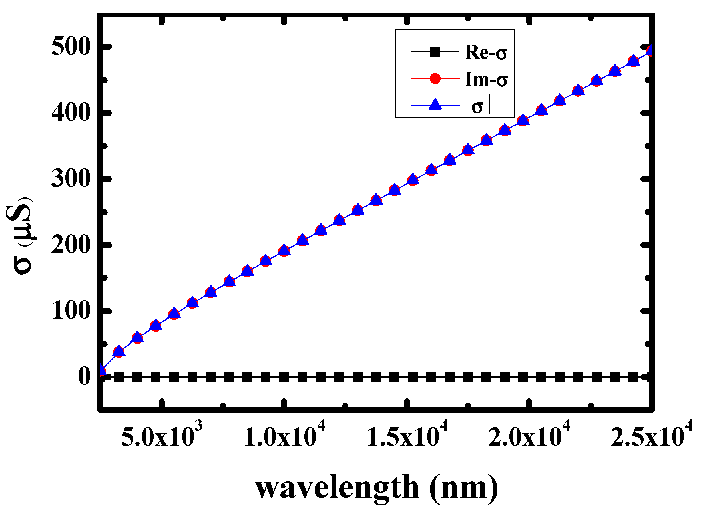
Figure 2 shows the relation between graphene’s electrical conductivity and incident wavelengths, where the graphene substrate material is Si, v = 1 V, and d = 10 nm.
The permittivity of graphene can be obtained from graphene’s electrical conductivity, as shown in Equation (6):
where w is the angular frequency of incident light. dg is the thickness of single-layer graphene.
Graphene in the structure presented here can be seen as a layer current. Combining Maxwell equations and the boundary conditions of Maxwell equations, the surface plasmon dispersion relation in TM mode (no magnetic field component in the direction of propagation) can be expressed using Equation (7):
where k1 and k2 are the longitudinal wave vectors of the SPPs’ wave in dielectric mediums of the top and bottom layers, which meet the equation km2 = β2 − εmk02, where m = 1, 2 and β is the propagation constant of the SPPs. The real part of k1 and k2 can effectively indicate the attenuation of the wave from the interface to the medium internal. When the top and bottom layers of graphene are the same material, assuming ε1 = ε2 = ε, the dispersion relation of graphene can be simplified as in the following equation:
where η0 = 377 ohms is intrinsic wave impedance in free space. K0 is the propagation constant of an electromagnetic wave in air. The propagation length of graphene SPPs (Lg) is defined as the distance at which the electric field intensity attenuates to 1/e of the initial electric field intensity, which is mainly dependent on the imaginary part of β and can be expressed as Lg = l / Im (β).
It can be seen from the above equations that the dispersion characteristics of graphene can be regulated by changing the applied voltage, substrate thickness, and substrate material, so as to regulate the transmission characteristics of graphene SPPs’ wave.
4. Results and Discussion
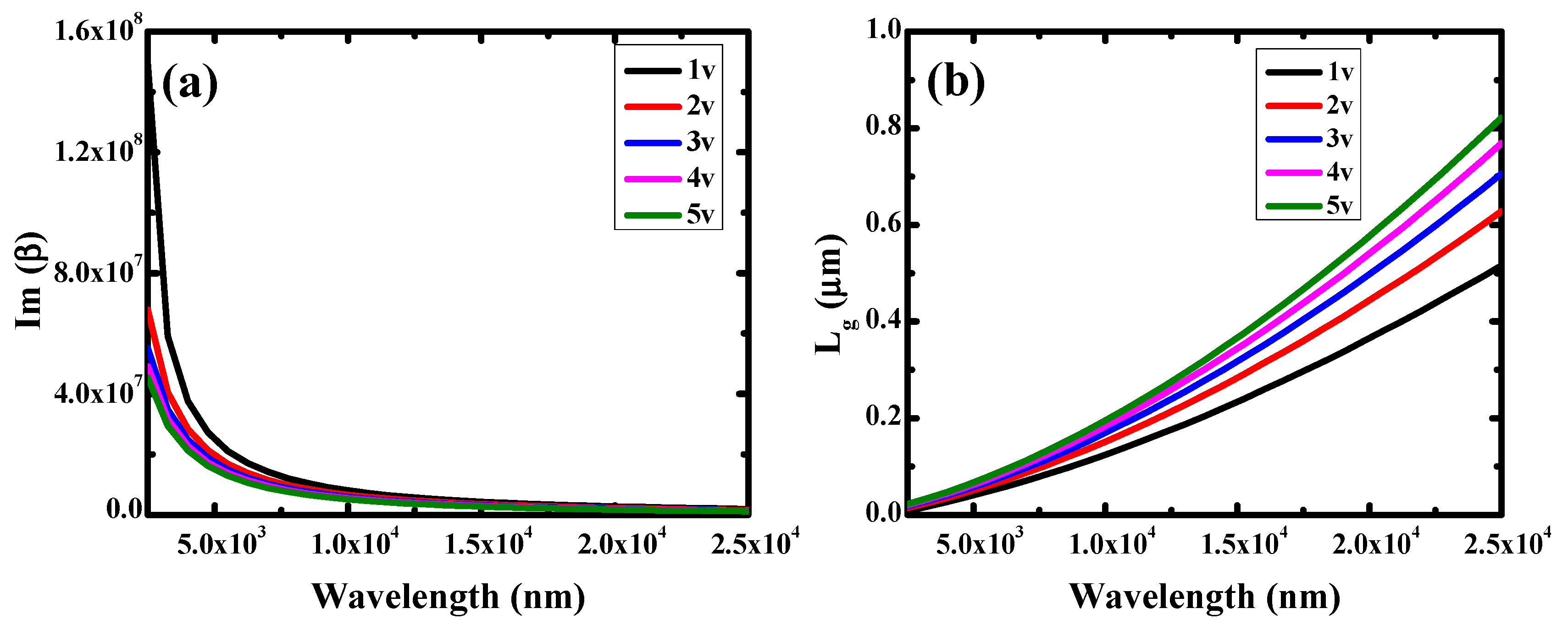
Figure 3 shows the transmission characteristics on incident wavelengths for different applied voltages (1, 2, 3, 4, and 5 V), and the incident wave is in the mid-infrared region (2500–25,000 nm). Here, Si is selected as the graphene substrate and dielectric material, and the substrate thickness is 10 nm. As shown in Figure 3, with the increase of the incident wavelength, the imaginary part of β decreases and the transmission distance increases, revealing the reduction of transmission loss with increasing wavelength. It can be seen in Figure 3 that the voltage applied to graphene has a great influence on the transmission characteristics of SPPs, enabling the realization of voltage-tunable SPPs. This is mainly due to the increasing electrical conductivity of graphene caused by the changing voltage applied to graphene.
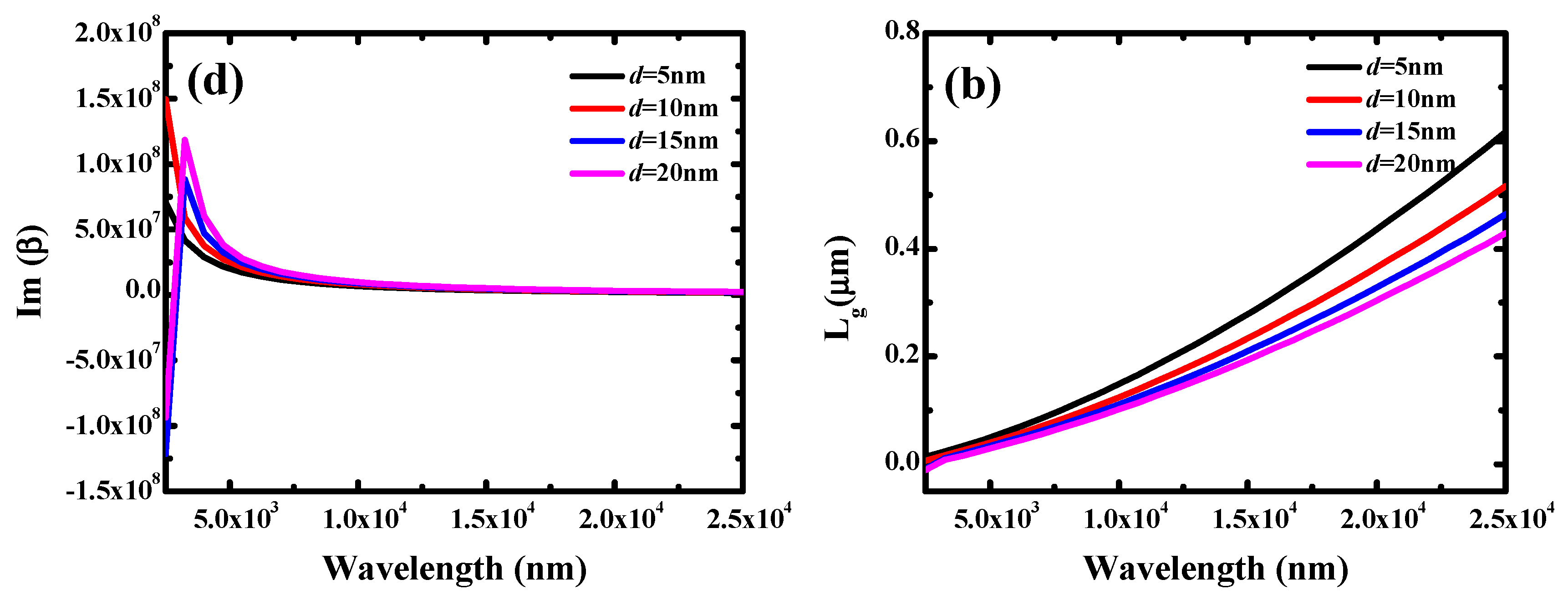
Next, the effect of different substrate thicknesses (5, 10, 15, and 20 nm) on the transmission performance of graphene SPPs in the mid-infrared region was explored. Here, substrate and dielectric material is Si, and v = 1 V. Figure 4 reveals that Im(β) decreases and Lg increases with the increasing wavelength. Meanwhile, the thinner the substrate, the longer the propagation length. These results are mainly attributed to the changing graphene chemical potential caused by a changing substrate thickness. As shown in Figure 4, Lg and Im(β) are both negative at the substrate thicknesses of 15 and 20 nm when the wavelength is less than a certain value, which is because graphene SPPs cannot be excited under these conditions.
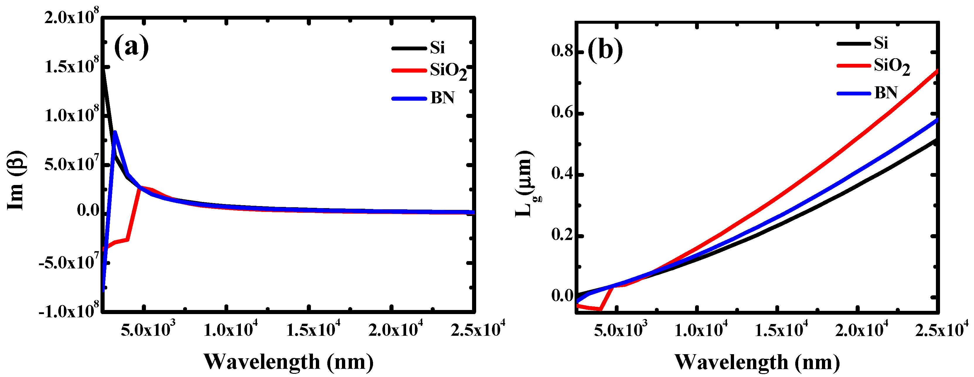
Figure 5 shows the transmission characteristics of graphene SPPs on incident wavelengths for different substrate and dielectric materials (Si, SiO2, and BN). Here, d = 10 nm and v = 1 V. Figure 5 illustrates that different substrate materials have a strong influence on the transmission properties of graphene SPPs. Smaller transmission loss and longer transmission length can be caused by a smaller dielectric constant of the substrate material. As shown in Figure 5, Lg and Im(β) are both negative for the substrate materials SiO2 and BN when the wavelength is less than a certain value, because graphene SPPs cannot be excited under these conditions. Comparing the transmission characteristics with those of other materials, SiO2 is a superior substrate material.
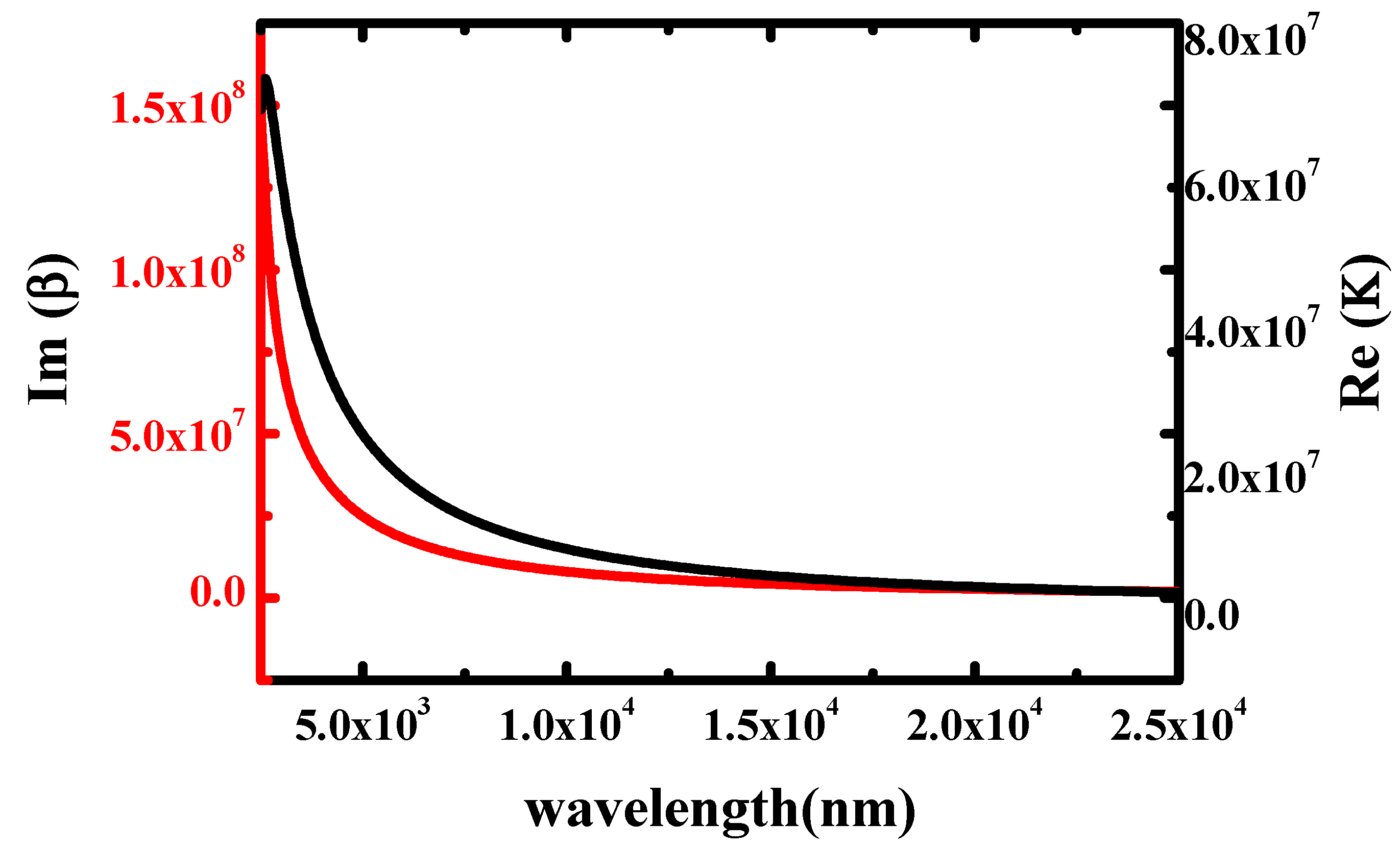
Figure 6 shows the influence of Im(β) and the real part of the longitudinal wave vector Re(k) on incident wavelengths. Re(k) can effectively indicate the attenuation of the incident wave from the interface to the internal medium, and Im(β) represents the transmission loss of graphene SPPs. Here, the substrate material is Si, d = 10 nm, and v = 1 V. As revealed in Figure 6, Im(β) and Re(k) have the same changing trend with the increase of the incident wavelength, which explains why a long propagation distance is usually accompanied with a really weak mode confinement, and vice versa.
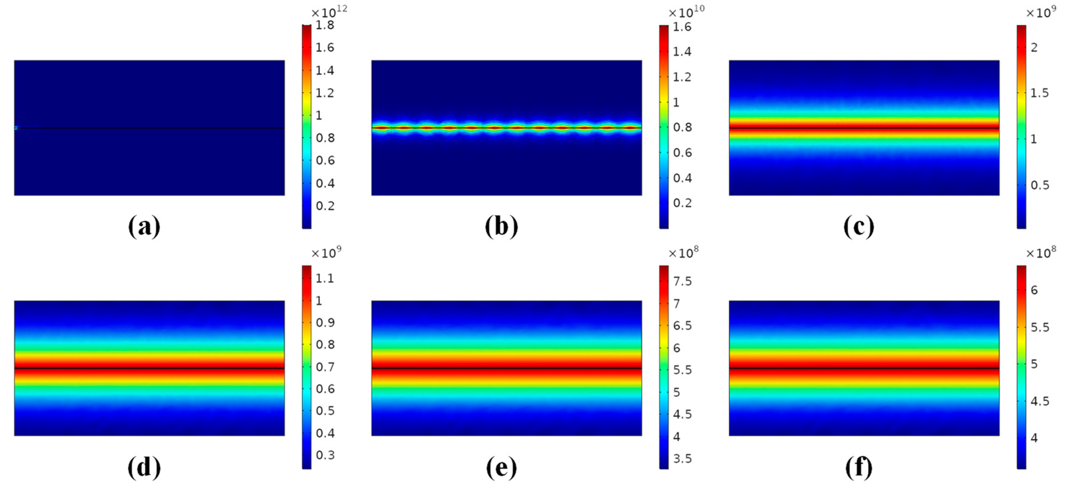
In order to further confirm the above conclusions, the transmission properties of proposed structure were investigated numerically using the finite element method (FEM) package in the RF module of COMSOL Multiphysics software (COMSOL company, Stockholm, Sweden). The convergence analysis was applied to ensure that the meshing and boundary conditions employed in the models were reasonable. The simulation model used is shown in Figure 1, and the sizes in the x, y, z directions are 150, 600, and 300 nm, respectively. The substrate material is Si, d = 10 nm, and v = 1 V. Figure 7 shows the effect of electric field distributions in the direction of light transmission (z direction) on different incident wavelengths. It can be seen from Figure 7 that the incident wavelength of 2500 nm cannot excite graphene SPPs under these conditions. The mode confinement becomes weaker and longitudinal attenuation of light decreases with the increasing incident wavelength, which is mainly attributed to the decrease of Re(k). These results are consistent with the results of Figure 6 above.
All of the simulation results above confirm the unique performance of graphene SPPs in the mid-infrared region. The transmission characteristics of graphene SPPs can be regulated by changing the applied voltage, substrate thickness, and substrate material. The properties of subwavelength operation and dynamic tunability make graphene the material with the most potential for application in optoelectronic devices. Moreover, this material outperforms metal SPPs and traditional silicon-based optoelectronic devices.
5. Conclusions
Through theoretical derivation and software simulation, the excellent transmission characteristics of graphene SPPs in the mid-infrared band were analyzed and verified effectively in this paper, and a sandwich waveguide structure of dielectric–graphene–substrate–dielectric based on graphene SPPs was presented. The dependence of the transmission characteristics on incident wavelengths for different substrate materials, different substrate thicknesses, and different applied voltages was obtained in this paper. This work is of great significance to further research of optical devices based on graphene SPPs in the mid-infrared region. Owing to their remarkable transmission properties, graphene SPPs can be used to manufacture subwavelength devices and represent the material with the most potential for the possible realization of VLSI.
Author Contributions
Y.W. conceived and designed the device; Y.W. and M.C. performed the numerical simulations; L.M. analyzed the data; H.L. and S.W. gave the guidelines for the paper; Y.W. wrote the paper with input from all authors.
Funding
This research is supported by the National Natural Science Foundation of China (Grant Nos. 61376099, 61434007, and 61504100) and 111 Project (B12026).
Conflicts of Interest
The authors declare no conflict of interest.
References
- Bian, Y.S.; Ren, Q.; Kang, L.; Yue, T.W.; Werner, P.L.; Werner, D.H. Deep-subwavelength light transmission in hybrid nanowire-loaded silicon nano-rib waveguides. Photonics Res. 2018, 6, 37–45. [Google Scholar] [CrossRef]
- Luo, S.; Wang, Y.; Tong, X.; Wang, Z. Graphene-based optical modulators. Nanoscale Res. Lett. 2015, 10, 199. [Google Scholar] [CrossRef] [PubMed]
- Qiu, P.P.; Qiu, W.B.; Lin, Z.L.; Chen, H.B.; Ren, J.B.; Wang, J.X.; Kan, Q.; Pan, J.Q. Dynamically Tunable Plasmon-Induced Transparency in On-chip Graphene-Based Asymmetrical Nanocavity-Coupled Waveguide System. Nanoscale Res. Lett. 2017, 12, 374. [Google Scholar] [CrossRef] [PubMed] [Green Version]
- Liu, F.; Zhang, X. Surface-Plasmon-Polariton Diode by Asymmetric Plano-Concave Nanocavities. Adv. Opt. Mater. 2018, 6, 1701226. [Google Scholar] [CrossRef]
- Patskovsky, S.; Kabashin, A.V.; Meunier, M.; Luong, J.H. Silicon-based surface plasmon resonance sensing with two surface plasmon polariton modes. Appl. Opt. 2003, 42, 6905–6909. [Google Scholar] [CrossRef] [PubMed]
- Zayats, A.V.; Smolyaninov, I.I.; Maradudin, A.A. Nano-optics of surface plasmon polaritons. Phys. Rep. 2005, 408, 131–314. [Google Scholar] [CrossRef]
- Moiseev, S.G.; Dadoenkova, Y.S.; Kadochkin, A.S.; Fotiadi, A.A.; Svetukhin, V.V.; Zolotovskii, I.O. Generation of Slow Surface Plasmon Polaritons in a Complex Waveguide Structure with Electric Current Pump. Ann. Phys. 2018, 11, 1800197. [Google Scholar] [CrossRef]
- Su, Y.; Lin, Q.; Zhai, X.; Wang, L.L. Enhanced Confinement of Terahertz Surface Plasmon Polaritons in Bulk Dirac Semimetal-Insulator-Metal Waveguides. Nanoscale Res. Lett. 2018, 13, 308. [Google Scholar] [CrossRef]
- Weber, G.M.; Maradudin, A.A. A Thin Phase Screen Model for Surface Plasmon Polaritons. Plasmonics 2019, 1–9. [Google Scholar] [CrossRef]
- Williams, C.R.; Andrews, S.R.; Maier, S.A.; Fernández-Domínguez, A.I.; Martín-Moreno, L.; García-Vidal, F.J. Highly confined guiding of terahertz surface plasmon polaritons on structured metal surfaces. Nat. Photonics 2008, 2, 175–179. [Google Scholar] [CrossRef]
- Liu, W.; Wei, J.; Sun, X.; Yu, H. A Study on Graphene-Metal Contact. Cryst. 2013, 3, 257–274. [Google Scholar] [CrossRef]
- Xu, Y.L.; Yu, H.J.; Wang, C.; Cao, J.; Chen, Y.G.; Ma, Z.Q.; You, Y.; Wan, J.X.; Fang, X.H.; Chen, X.Y. Multilayer Graphene with Chemical Modification as Transparent Conducting Electrodes in Organic Light-Emitting Diode. Nanoscale Res. Lett. 2017, 12, 254. [Google Scholar] [CrossRef] [PubMed]
- Bartolomeo, A.D.; Giulileo, F.; Luongo, G.; Lemmo, L.; Martucciello, N.; Niu, G.; Fraschke, M.; Skibitzki, O.; Schroeder, T.; Lupina, G. Tunable Schottky barrier and high responsivity in graphene/Si-nanotip optoelectronic device. 2d Mater. 2016, 4, 015024. [Google Scholar] [CrossRef] [Green Version]
- Lee, D.; Ahn, H.L.Y.; Jeong, Y.; Lee, D.Y.; Lee, Y. Highly stable and flexible silver nanowire-graphene hybrid transparent conducting electrodes for emerging optoelectronic devices. Nanoscale 2013, 5, 7750–7755. [Google Scholar] [CrossRef]
- Wang, X.; Cheng, Z.; Xu, M.; Tsang, H.K.; Xu, J.B. High-responsivity graphene/silicon-heterostructure waveguide photodetectors. Nat. Photonics 2013, 7, 888–891. [Google Scholar] [CrossRef]
- Li, H.; Anugrah, Y.; Koester, S.J.; Li, M. Optical absorption in graphene integrated on silicon waveguides. Appl. Phys. Lett. 2012, 101, 611–622. [Google Scholar] [CrossRef]
- Zolotovskii, I.O.; Dadoenkova, Y.S.; Moiseev, S.G.; Kadochkin, A.S.; Svetukhin, V.V.; Fotiadi, A.A. Plasmon-polariton distributed-feedback laser pumped by a fast drift current in graphene. Phys. Rev. A. 2018, 97, 053828. [Google Scholar] [CrossRef]
- Li, X.; Tu, Z.; Jin, Q.; Gao, S.; He, S. Broadband spectra translation between mid-infrared band and telecom band in a nonlinear silicon-based symmetric hybrid plasmonic waveguide. J. Nonlinear Opt. Phys. Mater. 2018, 27, 1850022. [Google Scholar] [CrossRef]
- Evseev, D.A.; Sementsov, D.I. Surface Plasmon Polaritons at the Boundary of a Graphene-Based Thin-Layer Medium. Phys. Solid State 2018, 60, 616–621. [Google Scholar] [CrossRef]
- Wang, W.H.; Zhou, W.J.; Fu, T.; Wu, F.; Zhang, N.; Li, Q.F.; Xu, Z.F.; Liu, W.H. Reduced propagation loss of surface plasmon polaritons on Ag nanowire-Graphene hybrid. Nano Energy 2018, 48, 197–201. [Google Scholar] [CrossRef]
- Liu, S.G.; Zhang, C.; Hu, M.; Chen, X.X.; Zhang, P.; Gong, S.; Zhao, T.; Zhong, R.B. Coherent and tunable terahertz radiation from graphene surface plasmon polaritons excited by an electron beam. Appl. Phys. Lett. 2014, 104, 109. [Google Scholar] [CrossRef]
- Xu, G.; Ming, C.; Chang, L.; Jian, S.; Tao, P. Tunable surface plasmon-polaritons in a gyroelectric slab sandwiched between two graphene layers. Opt. Commun. 2016, 366, 112–118. [Google Scholar] [CrossRef]
- Soriano-Disla, J.M.; Janik, L.J.; Rossel, R.A.V.; Macdonald, L.M.; Mclaughlin, M.J. The Performance of Visible, Near-, and Mid-Infrared Reflectance Spectroscopy for Prediction of Soil Physical, Chemical, and Biological Properties. Appl. Spectrosc. Rev. 2014, 49, 139–186. [Google Scholar] [CrossRef]
- Kuzmin, D.A.; Bychkov, I.V.; Shavrov, V.G.; Temnov, V.V. Plasmonics of magnetic and topological graphene-based nanostructures. Nanophotonics 2018, 7, 597. [Google Scholar] [CrossRef]
- Wu, Y.; Dai, X.; Xiang, Y.; Fan, D. Nonlinear TE-polarized SPPs on a graphene cladded parallel plate waveguide. J. Appl. Phys. 2017, 121, 103103. [Google Scholar] [CrossRef]
- Xu, Z.; Wu, D.; Liu, Y.M.; Liu, C.; Yu, Z.Y.; Yu, L.; Ye, H. Design of a Tunable Ultra-Broadband Terahertz Absorber Based on Multiple Layers of Graphene Ribbons. Nanoscale Res. Lett. 2018, 13, 143. [Google Scholar] [CrossRef] [Green Version]
- Yan, F.; Li, L.; Wang, R.X.; Tian, H.; Liu, J.L.; Liu, J.Q.; Tian, F.J.; Zhang, J.Z. Ultrasensitive Tunable Terahertz Sensor with Graphene Plasmonic Grating. J. Lightwave Technol. 2019, 37, 1103–1112. [Google Scholar] [CrossRef]
- Sui, K.; Ye, L.; Miao, Z.; Liu, Q.H.; Liu, Y. Graphene-based hybrid plasmonic waveguide for highly efficient broadband mid-infrared propagation and modulation. Opt. Express 2018, 26, 15935. [Google Scholar]
- Asgari, S.; Granpayeh, N. Applications of Tunable Nano-Scale Mid-Infrared Graphene-Based Slot Cavity in Nano photonic Integrated Circuits. IEEE Trans. Nanotechnol. 2018, 17, 533–542. [Google Scholar] [CrossRef]
- Li, J.; Zhang, T.; Chen, L. High-Efficiency Plasmonic Third-Harmonic Generation with Graphene on a Silicon Diffractive Grating in Mid-infrared Region. Nanoscale Res. Lett. 2018, 13, 338. [Google Scholar] [CrossRef]
- Cai, M.; Wang, S.; Gao, B.; Wang, Y.; Han, T.; Liu, H. A New Electro-Optical Switch Modulator Based on the Surface Plasmon Polaritons of Graphene in Mid-Infrared Band. Sens. 2019, 19, 89. [Google Scholar] [CrossRef] [PubMed]
- Qu, S.; Ma, C.; Liu, H. Tunable graphene-based hybrid plasmonic modulators for subwavelength confinement. Sci. Rep. 2017, 7, 5190. [Google Scholar] [CrossRef] [PubMed]
Figure 1.
The stereograph view of the proposed waveguide structure: (a) 3D layout waveguide structure; (b) cross-section structure.
Figure 1.
The stereograph view of the proposed waveguide structure: (a) 3D layout waveguide structure; (b) cross-section structure.

Figure 2.
Dependence of conductivity on incident wavelengths.

Figure 3.
Dependence of transmission characteristics on incident wavelengths for different applied voltages: (a) the imaginary part of β; (b) the propagation length (Lg).
Figure 3.
Dependence of transmission characteristics on incident wavelengths for different applied voltages: (a) the imaginary part of β; (b) the propagation length (Lg).

Figure 4.
Dependence of transmission characteristics on incident wavelengths for different substrate thicknesses (d): (a) the imaginary part of β; (b) the propagation length (Lg).
Figure 4.
Dependence of transmission characteristics on incident wavelengths for different substrate thicknesses (d): (a) the imaginary part of β; (b) the propagation length (Lg).

Figure 5.
Dependence of transmission characteristics on incident wavelengths for different substrate materials: (a) the imaginary part of β; (b) the propagation length (Lg).
Figure 5.
Dependence of transmission characteristics on incident wavelengths for different substrate materials: (a) the imaginary part of β; (b) the propagation length (Lg).

Figure 6.
Dependence of the imaginary part of propagation constant (β) and the real part of longitudinal wave vector (k) on incident wavelengths.
Figure 6.
Dependence of the imaginary part of propagation constant (β) and the real part of longitudinal wave vector (k) on incident wavelengths.

Figure 7.
Electric field distributions of the proposed transmission structure on different incident wavelengths: (a) 2500 nm; (b) 5000 nm; (c) 10,000 nm; (d) 15,000 nm; (e) 20,000 nm; (f) 25,000 nm.
Figure 7.
Electric field distributions of the proposed transmission structure on different incident wavelengths: (a) 2500 nm; (b) 5000 nm; (c) 10,000 nm; (d) 15,000 nm; (e) 20,000 nm; (f) 25,000 nm.

© 2019 by the authors. Licensee MDPI, Basel, Switzerland. This article is an open access article distributed under the terms and conditions of the Creative Commons Attribution (CC BY) license (http://creativecommons.org/licenses/by/4.0/).
Share and Cite
MDPI and ACS Style
Wang, Y.; Liu, H.; Wang, S.; Cai, M.; Ma, L. Optical Transport Properties of Graphene Surface Plasmon Polaritons in Mid-Infrared Band. Crystals 2019, 9, 354. https://0-doi-org.brum.beds.ac.uk/10.3390/cryst9070354
AMA Style
Wang Y, Liu H, Wang S, Cai M, Ma L. Optical Transport Properties of Graphene Surface Plasmon Polaritons in Mid-Infrared Band. Crystals. 2019; 9(7):354. https://0-doi-org.brum.beds.ac.uk/10.3390/cryst9070354
Chicago/Turabian StyleWang, Yindi, Hongxia Liu, Shulong Wang, Ming Cai, and Lan Ma. 2019. "Optical Transport Properties of Graphene Surface Plasmon Polaritons in Mid-Infrared Band" Crystals 9, no. 7: 354. https://0-doi-org.brum.beds.ac.uk/10.3390/cryst9070354
Note that from the first issue of 2016, this journal uses article numbers instead of page numbers. See further details here.