Phase and Residual Stress Evaluation of Dual-Phase Al70Cr30N and Al80Cr20N PVD Films


1
Kennametal GmbH, Altweiherstr. 27, 91320 Ebermannstadt, Germany
2
Kennametal Inc., 1600 Technology Way, Latrobe, PA 15650, USA
*
Author to whom correspondence should be addressed.
Crystals 2019, 9(7), 362; https://0-doi-org.brum.beds.ac.uk/10.3390/cryst9070362
Submission received: 5 June 2019
/
Revised: 30 June 2019
/
Accepted: 10 July 2019
/
Published: 15 July 2019
(This article belongs to the Special Issue X-ray and neutron Line Profile Analysis of Microstructures)
Abstract
:We investigated arc ion-plated Al70Cr30N and Al80Cr20N thin films deposited with three different bias voltages (50 V, 100 V, and 150 V) to study crystal phase stabilities, residual stresses, and mechanical properties. Commercial compositions of AlxCr100–xN coatings typically range from x = 50 to 70 where the cubic face centered crystal phase occurs. The present study focuses on films near the solubility limit of Al in the cubic Cr(Al)N lattice around 70 at.%, above which hexagonal AlN (h–AlN) starts to form in significant amounts. Residual stress values are obtained by two methods: grazing incidence diffraction with the wholepattern fitting and the conventional side inclination method (sin2Ψ method). When multiple phases are present in the film, wholepattern fitting turns out to be particularly effective and a comparison of both measurement methods will be discussed. The Al70Cr30N films consist of the cubic phase with crystallite sizes of about 70 nm for all bias voltages. Compressive stress increased with bias voltage from about 3 to almost 6 GPa and coatings become brittle. Al80Cr20N films showed a different dependence on bias voltage. Using 50 V bias voltage in deposition, the major phase is h–AlN phase with a crystallite grain size of < 30 nm and (0002) preferred orientation. With increasing bias the cubic phase is stabilized also reaching about 70 nm crystallite size. In general, the compressive residual stress was significantly lower than for Al70Cr30N films for the same bias voltages which may be a result of the presence of the hexagonal phase. Wear and scratch tests confirmed higher ductility of the Al80Cr20N variants but reduced resistance of the films in impact wear testing.
1. Introduction
Transition metal aluminum-enriched nitride films like TiAlN and AlCrN have been used as protective coatings in the metal cutting tool industry because of their excellent properties, such as high hardness and toughness [1,2,3]. Both coating systems share the same cubic base lattice. In this rocksalt structure (face-centered cubic), Al atoms may substitute Ti or Cr atoms on their respective sites. This leads to lattice distortion and stress build-up, but also to improved hardness and oxidation resistance [4]. The Cr—Al—N ternary system is of special interest since theoretical considerations indicate that CrN should be able to accommodate a higher amount of Al atoms (> 70 at.%) in the cubic phase than Ti—Al—N [5]. The properties of AlCrN films with cubic phase were studied extensively. Many authors have observed the transition from cubic to hexagonal phase at or slightly above 70 at.% Al in sputtered [6] and arc-evaporated films [7,8]. The bias voltage applied to the substrate is one of the main parameters in PVD since it controls the intensity of ion bombardment during film growth. Lomello et al. investigated the effect of the substrate bias voltage on Al60Cr40N films [9]. They observed a saturation at 100 V and a decrease of hardness and stress at 150 V bias voltage due to beginning delamination of the coating. Sabitzer et al. reported on bias voltage variation to keep the cubic phase stable when increasing the Al content above 70 at.% [10,11]. They deposited mono- and multi-layers through arc evaporation of Al90Cr10 and Al70Cr30 source materials (targets). By increasing the bias from 40 to 120 V, an increased share of cubic phase was observed for Al90Cr10N mono–layers. A multi–layered coating of Al90Cr10N and Al70Cr30N stacks with a layer thickness of about 40 nm resulted in a mainly cubic phased coating with high hardness values around 30 GPa.
In this work, we wanted to use a very similar approach but with much thinner layers. We achieved this by simply using the substrate table rotation which automatically results in nano-layers when using two different target compositions adjacent to each other. One focus of this contribution is to reveal the crystal phases of the resulting films by X-ray diffraction. Another aim was to prove that wholepattern fitting of 2Θ scans yields comparable stress values as the conventional but more time–consuming side inclination (or sin²ψ) method. Finally, we also wanted to explore the potential of dual-phase AlCrN coatings for wear protection. Recent results have indicated that coatings combining the favored cubic phase with low amounts of the softer hexagonal phase can be beneficial for tool life in the case of AlTiN coatings [12], and the same should hold true for AlCrN thin films.
2. Materials and Methods
2.1. Coating Deposition
Coating deposition was done using an industrial scale PVD cathodic arc unit (Oerlikon Balzers “Innova”, Balzers, Liechenstein) using four circular evaporators consisting of round “target” plates with a diameter of 120 mm. Powder–metallurgically prepared Al70Cr30 and Al90Cr10 targets with 99.8% purity were used (supplier: GFE Materials, Nuremberg, Germany). The evaporators are equipped with a permanent magnet on the back to stabilize arc movement. The films were deposited in a nitrogen atmosphere at a pressure of 3.5 Pa. The chamber was kept at a constant temperature of 480 °C. Arc evaporator current was set at 150 A for each source. The deposition time was kept constant at 150 min for all variants. Table 1 lists the six variants that were studied with respect to changing bias voltage and chemical composition. The resulting thickness varied in a range between 1.3 and 1.9 µm. Al70Cr30N variants were deposited using four Al70Cr30 targets whereas the Al80Cr20N coatings were obtained by using two of each, Al70Cr30 and Al90Cr10 targets. As samples are mounted on a turntable that rotates at approximately 1 rev/min this arrangement leads to a nano-layered film when using different source materials. Nominally, 0.01 µm or 10 nm are deposited during each revolution, and a nominal thickness of 5 nm per Al70Cr30N and Al90Cr10N layer is expected.
Square turning inserts SNMA120408 of ISO K10-grade (Kennametal, Latrobe, PA, USA) cemented carbide were used as substrates (composition: 6 wt.% Co binder, remainder WC). Samples were prepared by grinding, dry-blasting with alumina grit, and washing before coating. The coating process consisted of heating, anode assisted plasma etching (with argon gas), coating, and cooling resulting in a total process time of about 4 h.
2.2. Coating Analysis
Coating thickness was determined by calotte grinding about 1 mm away from the sample edge. Coating adhesion on the substrates was evaluated by scratching with a Rockwell diamond tip in Revetest device (CSM, Neuchatel, Switzerland) The load increased by 2 N/s from 0 to 70 N along a distance of 7 mm. The test was done twice on two different flank surfaces to improve the statistical significance. Chemical composition of the films agreed well with source material composition and the mixture of them, respectively and was confirmed by EDS with a Phenom XL scanning electron microscope. Hardness and modulus of the films were determined by the nano-indentation method using a Fischerscope HM2000. This device uses the loading and unloading curve at highest penetration to calculate an indentation hardness HIT and modulus EIT (and related values) [13]. EIT is also referred to as reduced modulus Er and takes Poisson’s ratio into account (0.18 taken here for AlCrN). For better accuracy, coated surfaces were polished at a slight angle to reduce scatter of the loading curves when trying to measure on too rough surfaces. To keep the maximum indentation depth significantly smaller than the film thickness a load of 20 mN was used without dwell time at maximum load, which resulted in a typical penetration depth of about 0.15 µm.
The wear resistance of the coated substrates was evaluated by cyclic impact testing as described in [12]. A polished carbide ball with a diameter of 5 mm and similar hardness as the substrate (about 1700 HV0.05) was used for impacting on a given spot for up to 10,000 times and 20,000 times for selected variants. The carbide ball was rotated slightly after each test to minimize any effects of ball wear. Cycle time was 0.4 sec with a maximum load of 50 N. The resulting wear crater was documented by light microscopy at 500× magnification.
2.3. X-ray Diffraction
2.3.1. Phase Characterizations
X-ray analyses were performed with Cu Kα radiation (λ = 1.5418 Å) and 45 kV (40 mA) excitation using a PANalytical XPert MRD diffractometer (Malvern Panalytical, Almelo, The Netherlands). Since the film thickness was less than 2 μm, the Bragg Brentano symmetric diffraction geometry resolves low index peaks of the film material better since the penetration depth is still low but increases with incident angle [14]. At α = 10°, the signal from the substrate is becoming dominant. Therefore, grazing incidence with fixed α and scanning 2θ was used, yielding intense diffraction peaks of higher indexes. Line tube focus mode with a parabolic mirror was used to achieve a highly parallel beam, which helps to minimize the beam defocusing and spurious peak shift by misalignment of sample height and sample surface conditions. A 1/32° divergence slit with 4 mm mask and 0.04° soller slits were used to ensure X-rays being confined within the sample surface at given α. The spectra were taken up to 2θ = 100° for wholepattern fitting.
2.3.2. Residual Stress Analysis
The residual stress was extracted from grazing incidence data by applying a wholepattern fitting procedure using the MStruct software. Matej et al. demonstrated previously that Mstruct is capable of fitting diffraction data for TiO2 films quite well [15]. This method is particularly useful when multiple phases are present and the individual peak fit method cannot be used due to line broadening or vanishing peaks. This software tries to fit the 2Θ scan profile taking into account background signal, lattice parameters of expected phases, and even distortion by stress and common lattice defects. Reflections are analyzed by a Rietveld type method but using also the stiffness tensor values for different hkl (directions). The functioning and correct setting of the instrument was checked and parameterized using a LaB6 standard obtained from NIST. Stiffness tensors of ab initio calculations performed by Zhou et al. for AlxCr100−xN were used [16].
Conventional side inclination by variation of the X angle was performed to determine film stress using the slope of the lattice spacing against sin²ψ (Stress Plus software from PANalytical). However, in Θ/2Θ symmetric geometry with Eulerian cradle X angle tilt, only the low index reflections (111) and (200) could be used for studying the cubic phase due to rapid increase of the penetration depth and reduced signal intensity for higher indexed reflections. Elastic modulus values were taken from the nano-indentation measurements as an approximation of Young’s modulus. These values do not account for different hkl directions and add an additional error to the measured stress values. A Poisson’s ratio ν of 0.18 was used for the cubic AlCrN phase.
3. Results and Discussions
3.1. Mechanical Coating Properties
Table 2 contains an overview of the mechanical properties for all the samples studied. For the Al70Cr30N variants, HIT and EIT values are in the same range. In contrast, the values obtained for Al80Cr20N variants show an almost linear increase and reach the level of the Al70Cr30N variants at 150 V bias voltage. The hardness values agree fairly well with the ones reported by Sabitzer et al. [10]. In general, EIT and HIT values are closely connected, since their ratio stays almost constant around 0.07. This ratio is sometimes considered as a possible indicator of wear resistance [17]. The calculated ratios are slightly above the value of 0.06 reported by Varghese et al. for AlCrN but smaller than the value of 0.09 found by Romero et al. for CrAlN films [18,19].
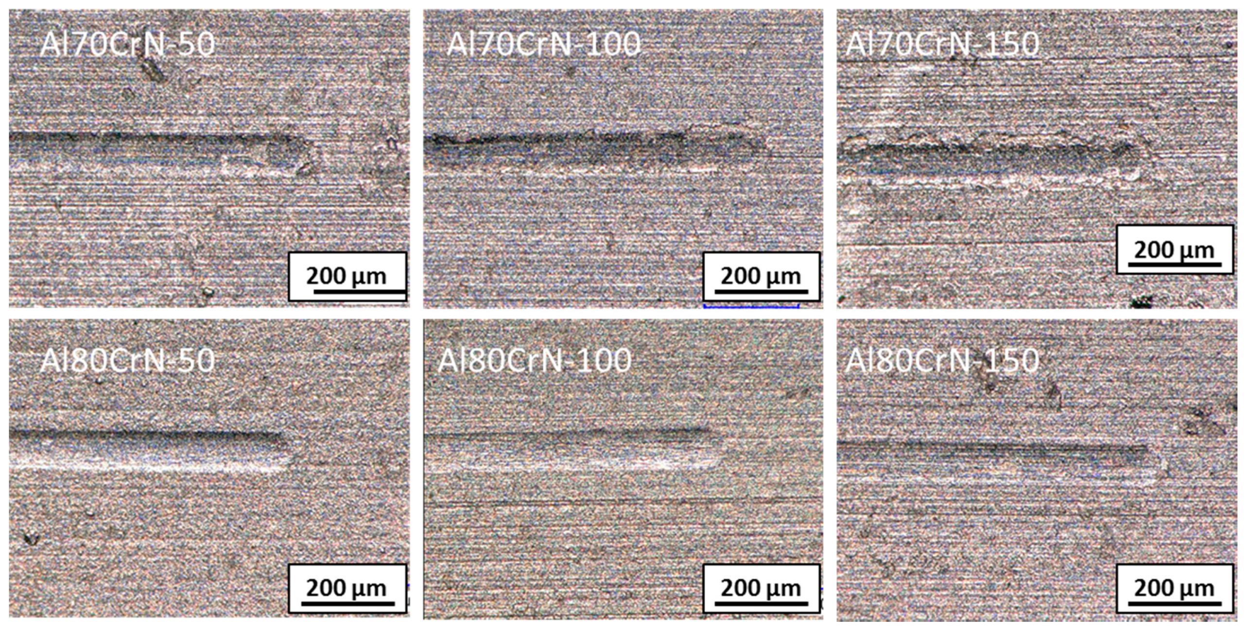
Figure 1 shows the end of sliding tracks after scratch testing. Most of the variants pass 70 N loading without coating delamination except variant Al70CrN–150, where coating failure occurs above 60 N. This is an indication of relatively high stress and a certain brittleness of this variant as described by Lomello et al. [9]. The tracks for the Al80Cr20N variants show a smooth contour, which indicates a softer coating. Even at highest bias there is no flaking of the coating, which is a significantly different behavior from that for variant Al70CrN–150. We consider this to be an indication of a higher toughness of the coating but could not support but mechanical testing data.
3.2. Phase Analysis
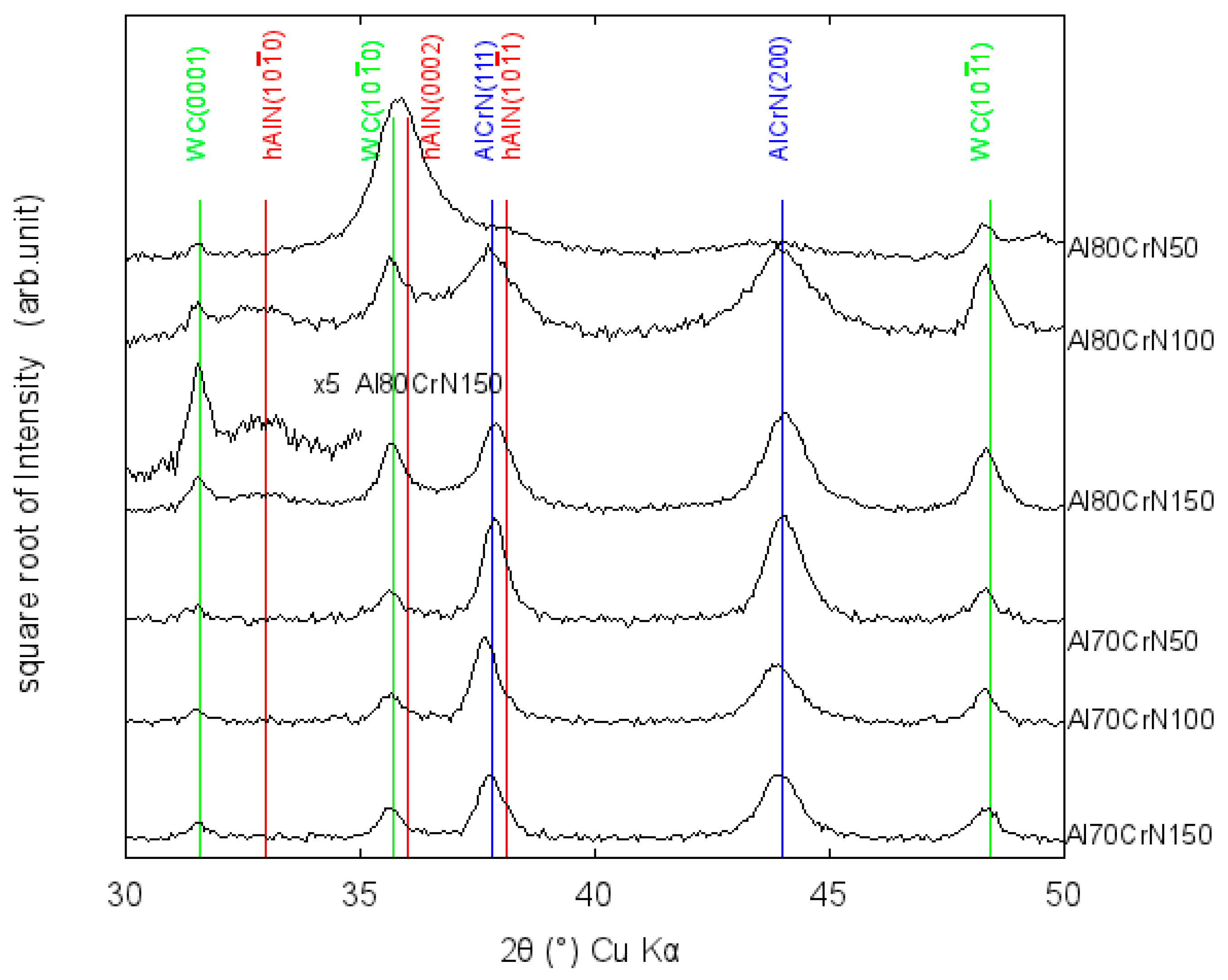
Figure 2 contains grazing incidence spectra for both variants deposited with three different bias voltages using an incidence angle of α = 1°. Reference reflections taken from ICDD file numbers 00–025–1047 (WC), 00–025–1133 (h–AlN), and 04–015–6218 (CrAlN) are displayed, as well. A small intensity from the WC substrate can be seen, which ensured the signal is from the entire thickness of the film. In the case of the Al70Cr30N variants, the peaks of the cubic CrAlN phase, hereafter denoted as “AlCrN”, occur near 2Θ values of 37–38° (111) and 44° (200). The crystallite size in these variants is estimated from the Williamson–Hall plot to be close to 70 nm. With increasing bias voltage, the peak intensity is reduced, and peaks get a little broader as expected. The grain size decreases as more defects and nucleation sites are formed under more intense ion bombardment. However, their intensity ratio stays almost constant, whereas Jäger et al. reported a change of from 111 to 200 preferred orientation when increasing bias for Al70Cr30N [20].
A significantly different 2Θ scan is obtained for the Al80CrN–050 sample. Only one dominant peak is observed near 36°, which can be identified as h–AlN (0002). Traces of the cubic AlCrN phase also seem to be present. When increasing the bias voltage from 100 to 150 V, the hexagonal phase shifts orientation from (0002) to (1010), as shown in the inset (5× magnification), and only the WC signal is left near 36°. The scans for variants Al80CrN–100 and, even more so, Al80CrN–150 resemble those of the Al70Cr30N variants, and the cubic phase with reflections at 37° at 43° becomes visible. The peaks also become narrower with higher bias voltage, which indicates an increase in crystal grain size. A very similar trend was described by Sabitzer et al. for Al70Cr30N/Al90Cr10N multi-layers with increasing bias. The authors explain the growth of cubic grains with the denser packed structure being favored under more severe ion bombardment [11].
3.3. Residual Stress Analysis
The films are expected to have compressive stress, since ion bombardment takes place during deposition because of the applied substrate bias voltage. Therefore, a simple Rietveld fit cannot extract correct lattice parameters from the grazing incidence data. Since the diffraction peaks are at ψ = Θ – α on the pole figure, grazing incidence geometry with constant α leads to different ψ for different hkl. For this reason, the shift of the diffraction peaks due to the residual stress needs to be included in the fit. We used the MStruct software for whole pattern fitting. MStruct is able to fit the entire scan, including all diffraction lines, thereby determining lattice distortion and associated stress values. A previous paper revealed good correlation with conventional single-peak fitting for coatings without strong texture or mixed phases [21]. Figure 3 shows representative wholepattern fits of three coating variants. Extending the scan to higher 2Θ angles up to 100° ensures better consideration of all phases present in the film. For example, Al80CrN–150 and Al80CrN–100 show h–AlN features at 33° and 58° for (1010) and (1120), respectively. Cubic AlCrN and WC substrate phases are included in the fit for Al70CrN–150 and additionally the h–AlN phase in the case of the Al80Cr20N variants. Lattice parameters, residual stress, stiffness tensor data were included as fit variables. Overall, a very good fit is obtained (red profile line). In the present case, (111) and (200) peaks from the cubic phases are relatively sharp and free from overlapping which allows using the conventional side inclination method to obtain residual stress values (except for Al80CrN–050, where only the cubic (200) signal could be used). However, when the overlap of peaks is significant, like in the Al80CrN–050 variant, it is hard to determine exact peak positions, and wholepattern fitting is the preferred method.
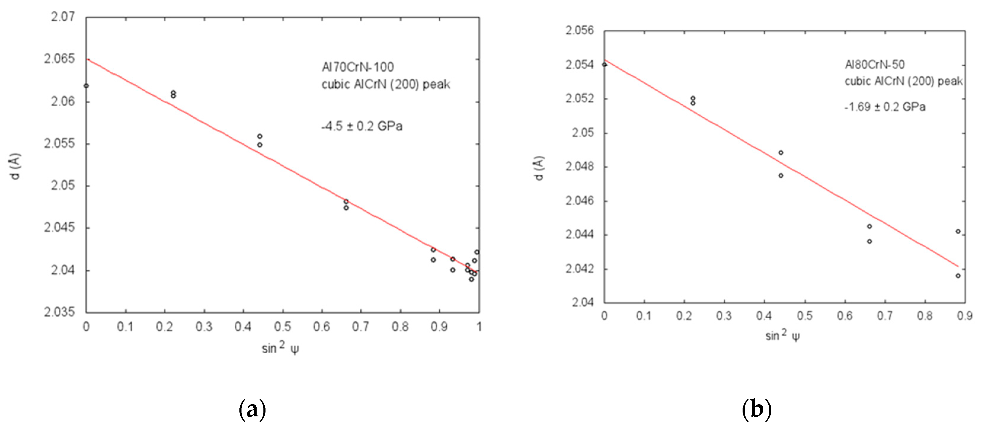
The stress of the films was first determined by the side inclination method (tilting the sample by an angle X). Only the cubic phase was taken for the evaluation, by plotting the lattice parameter d (which is known from the Bragg formula) over sin²ψ for cubic AlCrN peaks (111) and (200). As an example, Figure 4 shows representative d(sin²ψ) plots for Al70CrN–050 and Al80CrN–050 variants, respectively. It is obvious that there is a linear dependence, which indicates a homogeneous stress level over the entire coating depth. Note the higher scatter for Al80CrN–050 due to the very broad cubic (200) reflection.
Table 3 lists the compressive stress values obtained by the side inclination method and wholepattern fitting using the cubic phase. Several observations can be made. First, the stress values obtained for the cubic phase (111) and (200) reflections agree quite well. Also, wholepattern fitting results in somewhat higher absolute values for lower bias voltages. This is believed to result from the stiffness tensors taken from literature.
For the Al70Cr30N variants, the stress reaches a maximum around 6 GPa at 100 V bias voltage, whereas the Al80Cr20N coatings reveal an almost linear increase in compressive stress with higher bias. In general, Al80Cr20N variants show lower stress values than Al70Cr30N at comparable bias voltages. This could be explained by the presence of a hexagonal phase which seemingly relieves stress of the coatcubic phase. This view is supported by the stress value obtained for the Al80CrN–050 variant by evaluating the cubic (200) reflection and wholepattern fitting, which resulted in values around 1–2 GPa. Overall, the determined values are in a typical range and agree reasonably well with recently reported values [20].
Wholepattern fitting is particularly useful for films containing multiple phases with broad signals and contributions from the substrate and other phase (s). It is then often difficult to deconvolute XRD scans. As we have again shown here, at least for a coating with two phase and without vertical gradient, wholepattern fitting and the side inclination method are in reasonably good agreement.
3.4. Hexagonal AlN Phase
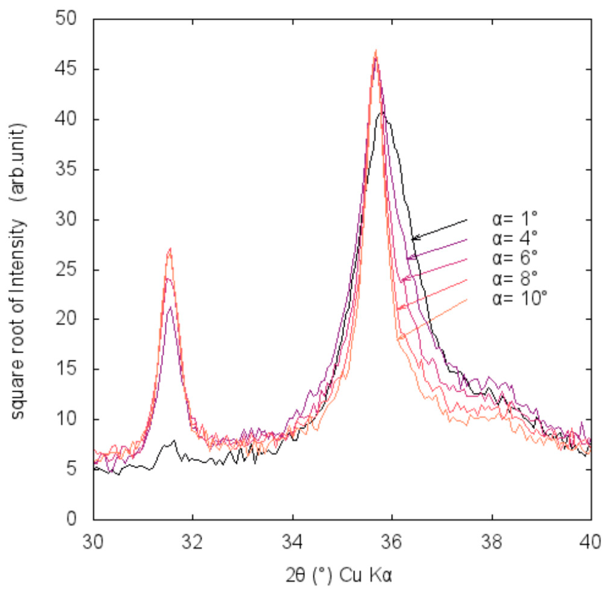
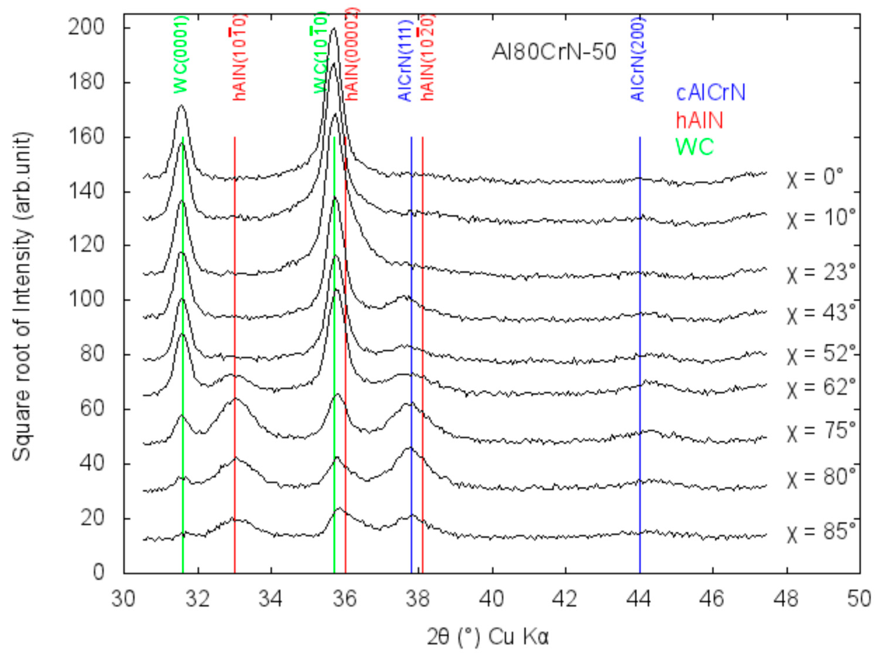
In a further step, the profile of Al80CrN–050 was studied in more detail. As shown in Figure 2, it reveals a significant amount of h–AlN phase, with the most intense peak near 2θ = 36° originating from AlN (0002) and some WC (1010) substrate signal. To better discriminate these signals, different grazing angles from 1 to 10° were used in scanning the range between 30 and 40° (2Θ). Figure 5 shows the resulting intensities with varying α. As the incident angle increases, the beam penetrates deeper and the substrate signal near 32 and 36° gets stronger. The signal at 36° is narrowed as the tail between 36 and 37° belonging to h–AlN (0002) fades away at higher incident angles as expected.
When taking the XRD scans using the X side inclination method for conventional stress measurement, it was noted that there is a texture in the h–AlN phase. Figure 6 shows 2Θ scans with X = 0–85°. It can be seen that the h–AlN (1010) peak, and likely also the (1120) peak, become clearly visible above 62° and seem to be linked to the cubic (111) plane, which is also visible above X = 40°. The h–AlN (0002) orientation is most intense around X = 20° and rises again above 80°. It is, therefore, likely that the orientation of the (0002) plane is tilted by some amount to the surface normal. In general, a 0002 preference for PVD of h–AlN was also reported by others [21,22], but the observed tilting cannot be explained well and needs further study.
3.5. Wear Testing
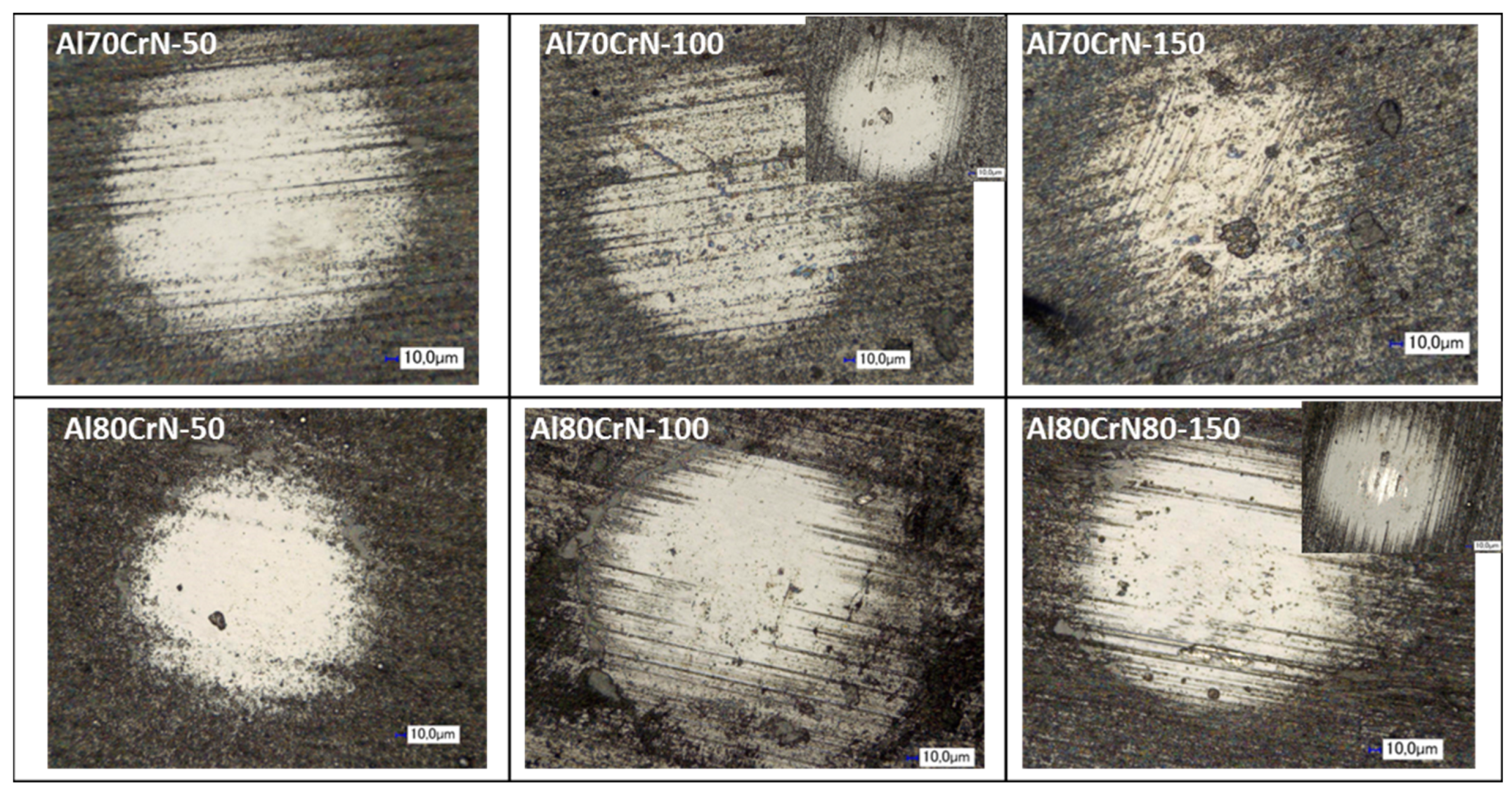
All six variants were subjected to a wear test by cyclic impacting. This test specifically evaluates coating adhesion, toughness, and fatigue resistance of the coating. Figure 7 shows the resulting impact craters after 10,000 impacts. For the Al70Cr30N series (upper row), coating delamination occurs for samples that were coated with increasing bias voltage. The variant with highest bias shows coating flaked off at some larger areas from about 10 to 30 microns in size. This confirms the impression obtained by scratch testing, and is attributed to a high stress value of 5 GPa. Interestingly, compressive stress was at a similar level as in the case of the variant with 100 V bias. Mechanical property data (Table 2) cannot fully explain this behavior, as they are quite close and must be attributed to differences in toughness (which could not be determined). The lower row shows the impact areas of the Al80Cr20N variants reveal different patterns. In the case of the lower bias variants, the grinding marks are less visible, which could be explained by a softer, more ductile coating. Some defects start to occur for the variant deposited with 150 V bias voltage, but there are only smaller spots with exposed substrates when compared to Al70CrN–150.
When subjecting the two most promising variants up to 20,000 impacts the Al80CrN–150 shows more wear than Al70CrN–100 (see insets for these variants in Figure 7). In a further test, the two favorable variants A70CrN–100 and Al80CrN–150 were impacted 20,000 times and the image is shown as an inset in Figure 7. It can be seen that the substrate area is starting to get exposed for Al80CrN–150 indicating some inferior performance compared to Al70CrN–100. The exposed area had a diameter of roughly 90 µm. This wear test seems to depend not only on “static” mechanical values like hardness and modulus but also on toughness and fatigue behavior of a coating which are difficult to measure for thin films. Determining these material properties is therefore highly desirable in order to explain wear test results better and to forecast coating performance.
4. Conclusions
Al70Cr30N and Al80Cr20N thin films were deposited by arc ion plating on carbide substrates, varying the substrate bias voltage (50, 100, 150 V). Whereas purely cubic phased Al70Cr30N coatings have been studied quite well, nano-layered dual-phase nitride films obtained by co-deposition from two different AlCr alloy sources have received much less attention. The resulting coatings were analyzed using nano-indentation, wear testing, and x-ray diffraction in grazing incidence geometry with a focus on crystal phase and residual stress evaluation. Wholepattern fitting provided quick and comparable results when compared to the conventional side inclination (sin²ψ) method for all variants. In the case of the Al70Cr30N coatings increasing the bias voltage in deposition had only minor effects on hardness, modulus, and micro-structure. All three coating variants showed comparable mechanical properties regardless with a hardness at or above 30 GPa and a modulus of about 440 GPa. A cubic crystal structure with grain sizes around 70 nm was determined for Al70Cr30N, and no hexagonal phase could be detected. Compressive residual stress doubles from about 3 to around 6 GPa with increasing bias voltage and the sin²ψ method and wholepattern fitting stress values agree reasonably well. At the highest bias voltages, the excessive ion bombardment at 150 V led to a brittle coating behavior under load. The Al80Cr20N coatings with Al70Cr30N and Al90Cr10N nano-layers behaved differently and showed a dual-phase micro-structure. In general, lower stress values were observed and could be explained by a relieved stress due to the presence of the hexagonal phase involving small grain size (many grain boundaries). The dominant phase at a low bias voltage of 50 V is hexagonal AlN with a preferred (0002) direction. Due to overlapping reflections, only wholepattern fitting allowed extraction of a stress value for the hexagonal phase. When increasing the substrate bias the formation of the cubic AlCrN phase is promoted with a grain size increase. The resulting diffraction pattern looks similar to the one obtained for Al70Cr30N. The Al80Cr20N variants showed on average 1–2 GPa lower compressive stress values at comparable bias voltages. This finding can be used to increase the bias voltage and associated hardness without compromising toughness and adhesion. This was proven by scratch and impact testing, which revealed a less brittle behavior and decreased tendency of adhesive coating failure. However, there seems to also be some inferior wear resistance of dual-phase Al80Cr20N coatings, and further investigation is necessary.
Author Contributions
T.S. carried out XRD experiments and analysis. J.K. performed deposition experiments and assessment of coating properties. Both authors contributed to the manuscript preparation.
Funding
This research was funded by INTERNAL R&D BUDGET.
Conflicts of Interest
The authors declare no conflict of interest.
References
- Endrino, J.L.; Fox–Rabinovich, G.S.; Gey, C. Hard AlTiN, AlCrN PVD coatings for machining of austenitic stainless steel. Surf. Coat. Technol. 2006, 200(24), 6840–6845. [Google Scholar] [CrossRef]
- Arndt, M.; Kacsich, T. Performance of new AlTiN coatings in dry and high speed cutting. Surf. Coat. Technol. 2003, 163–164, 674–680. [Google Scholar] [CrossRef]
- Liew, W.Y.H. Low-speed milling of stainless steel with TiAlN single-layer and TiAlN/AlCrN nano–multilayer coated carbide tools under different lubrication conditions. Wear 2010, 269, 617–631. [Google Scholar] [CrossRef]
- Chim, Y.C.; Ding, X.Z.; Zeng, X.T.; Zhang, S. Oxidation resistance of TiN, CrN, TiAlN and CrAlN coatings deposited by lateral rotating cathode arc. Thin Sol. Films 2009, 517, 4845–4849. [Google Scholar] [CrossRef]
- Makino, Y. Prediction of phase change in pseudobinary transition metal aluminum nitrides by band parameters method. Surf. Coat. Technol. 2005, 193, 185–191. [Google Scholar] [CrossRef]
- Makino, Y.; Nogi, K. Synthesis of pseudobinary Cr–Al–N films with B1 structure by rf–assisted magnetron sputtering method. Surf. Coat. Technol. 1998, 98, 1008–1012. [Google Scholar] [CrossRef]
- Reiter, A.E.; Derflinger, V.H.; Hanselmann, B.; Bachmann, T. Investigation of the properties of Al1−xCrxN coatings prepared by cathodic arc evaporation. Surf. Coat. Technol. 2005, 200, 2114–2122. [Google Scholar] [CrossRef]
- Mayrhofer, P.H.; Willmann, H.; Reiter, A.E. Structure and phase evolution of Cr–Al–N coatings during annealing. Surf. Coat. Technol. 2008, 202, 4935–4938. [Google Scholar] [CrossRef]
- Lomello, F.; Sanchette, F.; Schuster, F.; Tabarant, M.; Billard, A. Influence of bias voltage on properties of AlCrN coatings prepared by cathodic arc deposition. Surf. Coat. Technol. 2013, 225, 77–81. [Google Scholar] [CrossRef]
- Sabitzer, C.; Paulitsch, J.; Kolozsvári, S.; Rachbauer, R.; Mayrhofer, P.H. Influence of bias potential and layer arrangement on structure and mechanical properties of arc evaporated Al–Cr–N coatings. Vacuum 2014, 106, 49–52. [Google Scholar] [CrossRef]
- Sabitzer, C.; Paulitsch, J.; Kolozsvári, S.; Rachbauer, R.; Mayrhofer, P.H. Impact of bias potential and layer arrangement on thermal stability of arc evaporated Al–Cr–N coatings. Thin Sol. Films 2016, 610, 26–34. [Google Scholar] [CrossRef]
- Kohlscheen, J.; Bareiss, C. Effect of hexagonal phase content on wear behaviour of AlTiN arc PVD coatings. Coat. 2018, 8, 72. [Google Scholar] [CrossRef]
- Ullner, C. Hardness testing; Herrmann, K., Ed.; ASTM International: Materials Park, OH, USA, 2011; Chapter 6; p. 187. [Google Scholar]
- Birkholz, M.; Genzel, C. Thin film analysis by X–ray scattering; Birkholz, M., Ed.; Wiley VCH: Weinheim, Germany, 2006; Chapter 6; p. 273. [Google Scholar]
- Matej, Z.; Kuzel, R.; Nichtova, L. XRD total pattern fitting applied to study of microstructure of TiO2 films. Powder Diffr. 2010, 25, 125–131. [Google Scholar] [CrossRef]
- Zhou, L.; Holec, D.; Mayrhofer, P.H. First principles study of elastic properties of cubic Cr1–xAlxN alloys. J. Appl. Phys. 2013, 113, 043511. [Google Scholar] [CrossRef]
- Leyland, A.; Matthews, A. On the significance of the H/E ratio in wear control: A nanocomposite coating approach to optimised tribological behaviour. Wear 2000, 246, 1–11. [Google Scholar] [CrossRef]
- Varghese, V.; Akhil, K.; Ramesh, M.R.; Chakradhar, D. Investigation on the performance of AlCrN and AlTiN coated cemented carbide inserts during end milling of maraging steel under dry, wet and cryogenic environments. J. Manuf. Proc. 2019, 43, 136–144. [Google Scholar] [CrossRef]
- Romero, J.; Gomez, M.A.; Esteve, J.; Montala, F.; Carreras, L.; Grifol, M.; Lousa, A. CrAlN coatings deposited by cathodic arc evaporation at different substrate bias. Thin Solid Films 2006, 515, 113–117. [Google Scholar] [CrossRef]
- Jäger, N.; Klima, S.; Hruby, H.; Julin, J.; Burghammer, M.; Kecke, J.F.; Mitterer, C.; Daniel, R. Evolution of structure and residual stress of a fcc/hex–AlCrN multi–layered system upon thermal loading revealed by cross–sectional X–ray nano diffraction. Acta Mat. 2019, 162, 55–66. [Google Scholar] [CrossRef]
- Khan, S.; Shahid, M.; Mahmood, A.; Shah, A.; Ahmed, I.; Mehmood, M. Texture of the nano–crystalline AlN thin films and the growth conditions in DC magnetron sputtering. Progr. Nat. Sci. 2015, 25, 282–290. [Google Scholar] [CrossRef]
- Molleja, J.G.; Gomez, B.J.; Ferron, J.; Gautron, E.; Burgi, J.; Bassam, A.; Djouadi, M.A.; Feugeas, J.; Jouan, P.Y. AlN thin films deposited by DC reactive magnetron sputtering: Effect of oxygen on film growth. Eur. Phys. J. Appl. Phys. 2013, 64, 20302. [Google Scholar] [CrossRef]
Figure 1.
Scratch testing images at track end (load <= 70N) for all coating variants.

Figure 2.
XRD scans of all variants using grazing incidence angle diffracton at α = 1° with reference peak positions (taken from ICDD files, see text).
Figure 2.
XRD scans of all variants using grazing incidence angle diffracton at α = 1° with reference peak positions (taken from ICDD files, see text).

Figure 3.
Original diffraction data (black dots) and wholepattern fit (red line) for selected Al70Cr30N and Al80Cr20N variants (c = cubic AlCrN, s = substrate WC, h = hexagonal AlN).
Figure 3.
Original diffraction data (black dots) and wholepattern fit (red line) for selected Al70Cr30N and Al80Cr20N variants (c = cubic AlCrN, s = substrate WC, h = hexagonal AlN).

Figure 4.
Representative d(sin2Ψ) plots for the (200) peak of cubic CrAlN in Al70CrN–100 (a) and Al80CrN–050 (b).
Figure 4.
Representative d(sin2Ψ) plots for the (200) peak of cubic CrAlN in Al70CrN–100 (a) and Al80CrN–050 (b).

Figure 5.
XRD scans of sample Al80CrN–50 with variation of the incident angle α = 1–10°.

Figure 6.
XRD scans of sample Al80CrN–050 with variation of X angle (side inclination), vertical lines indicate reference peak positions as in Figure 2.
Figure 6.
XRD scans of sample Al80CrN–050 with variation of X angle (side inclination), vertical lines indicate reference peak positions as in Figure 2.

Figure 7.
Impact crater images after 10,000 impacts for all variants (insets at Al70CrN–100 and Al80CrN–150 show wear mark after 20,000 impacts).
Figure 7.
Impact crater images after 10,000 impacts for all variants (insets at Al70CrN–100 and Al80CrN–150 show wear mark after 20,000 impacts).


Table 1.
Overview of AlCrN variants deposited.
| x in AlxCr100–xN | Bias Voltage, V | Thickness, µm | Designation |
|---|---|---|---|
| 70 | 50 | 1.5 | Al70CrN–050 |
| 70 | 100 | 1.3 | Al70CrN–100 |
| 70 | 150 | 1.3 | Al70CrN–150 |
| 80 | 50 | 1.8 | Al80CrN–050 |
| 80 | 100 | 1.9 | Al80CrN–100 |
| 80 | 150 | 1.3 | Al80CrN–150 |
Table 2.
Mechanical properties of AlCrN variants.
| Designation | HIT (GPa) | EIT (Gpa) | HIT/EIT |
|---|---|---|---|
| Al70CrN–050 | 30 | 448 | 0.064 |
| Al70CrN–100 | 33 | 444 | 0.074 |
| Al70CrN–150 | 33 | 428 | 0.077 |
| Al80CrN–050 | 20 | 296 | 0.068 |
| Al80CrN–100 | 28 | 357 | 0.078 |
| Al80CrN–150 | 32 | 460 | 0.070 |
Table 3.
Residual stress values obtained by conventional side inclination for cubic (111) and (200) reflections and wholepattern (wp) fitting, all values in GPa.
Table 3.
Residual stress values obtained by conventional side inclination for cubic (111) and (200) reflections and wholepattern (wp) fitting, all values in GPa.
| Designation | Cubic 111 | Cubic 200 | wp Fit, Cubic | wp Fit, Hexag. |
|---|---|---|---|---|
| Al70CrN–050 | −2.6 ± 0.1 | −2.4 ± 0.9 | −3.0 ± 0.2 | |
| Al70CrN–100 | −5.6 ± 0.2 | −4.5 ± 0.2 | −6.5 ± 0.2 | |
| Al70CrN–150 | −5.2 ± 0.2 | −5.2 ± 0.1 | −5.4 ± 0.1 | |
| Al80CrN–050 | −1.7 ± 0.2 | −1.8 ± 0.3 | −0.7 ± 0.5 | |
| Al80CrN–100 | −3.5 ± 0.1 | −3.6 ± 0.3 | −4.3 ± 0.2 | |
| Al80CrN–150 | −4.1 ± 0.2 | −4.5 ± 0.2 | −4.5 ± 0.2 |
© 2019 by the authors. Licensee MDPI, Basel, Switzerland. This article is an open access article distributed under the terms and conditions of the Creative Commons Attribution (CC BY) license (http://creativecommons.org/licenses/by/4.0/).
Share and Cite
MDPI and ACS Style
Kohlscheen, J.; Shibata, T. Phase and Residual Stress Evaluation of Dual-Phase Al70Cr30N and Al80Cr20N PVD Films. Crystals 2019, 9, 362. https://0-doi-org.brum.beds.ac.uk/10.3390/cryst9070362
AMA Style
Kohlscheen J, Shibata T. Phase and Residual Stress Evaluation of Dual-Phase Al70Cr30N and Al80Cr20N PVD Films. Crystals. 2019; 9(7):362. https://0-doi-org.brum.beds.ac.uk/10.3390/cryst9070362
Chicago/Turabian StyleKohlscheen, Joern, and Tomohiro Shibata. 2019. "Phase and Residual Stress Evaluation of Dual-Phase Al70Cr30N and Al80Cr20N PVD Films" Crystals 9, no. 7: 362. https://0-doi-org.brum.beds.ac.uk/10.3390/cryst9070362
Note that from the first issue of 2016, this journal uses article numbers instead of page numbers. See further details here.