Deterministic Insertion of KTP Nanoparticles into Polymeric Structures for Efficient Second-Harmonic Generation


Laboratoire de Photonique Quantique et Moléculaire, UMR 8537, École Normale Supérieure Paris-Saclay, Centrale Supélec, CNRS, Université Paris-Saclay, 61 avenue de Président Wilson, 94235 Cachan, France
*
Author to whom correspondence should be addressed.
Crystals 2019, 9(7), 365; https://0-doi-org.brum.beds.ac.uk/10.3390/cryst9070365
Submission received: 27 May 2019
/
Revised: 20 June 2019
/
Accepted: 11 July 2019
/
Published: 17 July 2019
(This article belongs to the Special Issue Sonic and Photonic Crystals)
Abstract
:We investigate theoretically and experimentally the creation of virtually any polymer-based photonic structure containing individual nonlinear KTiOPO nanoparticles (KTP NPs) using low one-photon absorption (LOPA) direct laser writing (DLW) technique. The size and shape of polymeric microstructures and the position of the nonlinear KTP crystal inside the structures, were perfectly controlled at nanoscale and on demand. Furthermore, we demonstrated an enhancement of the second-harmonic generation (SHG) by a factor of 90 when a KTP NP was inserted in a polymeric pillar. The SHG enhancement is attributed to the resonance of the fundamental light in the cavity. This enhancement varied for different KTP NPs, because of the random orientation of the KTP NPs, which affects the light/matter interaction between the fundamental light and the NP as well as the collection efficiency of the SHG signal. The experimental result are further supported by a simulation model using Finite-Difference Time-Domain (FDTD) method.
1. Introduction
Second-harmonic generation (SHG) allows the generation of new photons with a double frequency () [1]. This is a second-order nonlinear optical process, thus does not provoke any absorption. Therefore, the SHG can avoid a bleaching effect and allows observations over long durations with no decrease in the signal quality, which is usually observed with fluorescent and luminescent nanoparticles (NPs) [2,3]. Moreover, the SH spectrum () is separated from the fundamental spectrum (), allowing spectrally filtering out the fundamental beam, resulting in an excellent contrast in nonlinear microscopy. In SHG process, a large range of excitation wavelengths can be used, depending on the nonlinear material used. Thus, for many applications, the fundamental wavelength can be selected in ranges where the absorption and scattering effects are low to avoid the losses and the photodegradation. This allows SHG to be observed in thick materials, which are very useful for bio-applications [4,5,6,7,8].
SHG could be performed with nonlinear materials at macro and micro scales. For some applications, such as biomarkers and nanosensors, nonlinear NPs should be used [4,8]. Several works have been devoted to fundamental studies of nonlinear properties of NPs, such as NPs of CMONS (Cyano-MethOxy-Nitro-Stilbene) [9,10,11] and hybrid organic/inorganic-based MnPS3 NPs [12]. Recently, Le Xuan et al. [2] have investigated KTiOPO (KTP) NPs, with the size in the range of 30 and 100 nm. This nonlinear crystal is commonly used due to its important nonlinear response and its transparency in visible and infrared ranges [13]. The nonlinear analyses of these NPs show that the SH signal is very high as compared to a massive KTP crystal and perfectly stable. The SHG of nonlinear NPs in general is efficient because no phase-matching is required, and those NPs could be easily functionalized with other materials, suggesting numerous applications particularly in the biology domain.
Direct laser writing (DLW) is an excellent method allowing fabrication of any one-, two-, and three-dimensional (1D, 2D, and 3D) structures at a sub-micrometer scale [14,15]. In this method, a femtosecond laser beam is usually used. The laser beam strongly focused into a photoresist by using a large numerical aperture (NA) objective lens (OL). Only the photoresist located inside the focusing spot is polymerized/depolymerized thanks to the multi-photon absorption (MPA) effect. An arbitrary structure then can be created by moving the focusing spot inside the photoresist. However, the MPA-based DLW is rather expensive and complicated since it requires a femtosecond laser and a complex optical system. Recently, a very simple and inexpensive technique called low one-photon absorption (LOPA) DLW is demonstrated as a robust technique [16,17], allowing realization of multidimensional structures as what realized by MPA-based DLW. In the LOPA setup, a simple and low-cost, continuous-wave (cw) and low power laser is used as an excitation laser, similar to the case of conventional OPA. However, this laser wavelength is located in an ultralow absorption range of the photoresist, thus can penetrate deeply inside the material. This LOPA effect is then compensated by the high intensity at the focusing spot, resulting in a compressed polymerized spot. By moving the focusing in 3D, any structure can be created as in the case of MPA-based DLW. Moreover, it was demonstrated that LOPA DLW technique enables the creation of desirable polymeric structures containing a single gold NP [18], that cannot be obtained by a standard MPA-based DLW.
In this work, we demonstrate the use of a modified LOPA system to embed a single KTP NP in a polymeric photonic structure in order to enhance the SHG of KTP NP as well as to manipulate the SH propagation.
2. Fabrication Procedure and Characterization of KTP NPs
2.1. Lopa-Based Dlw Setup
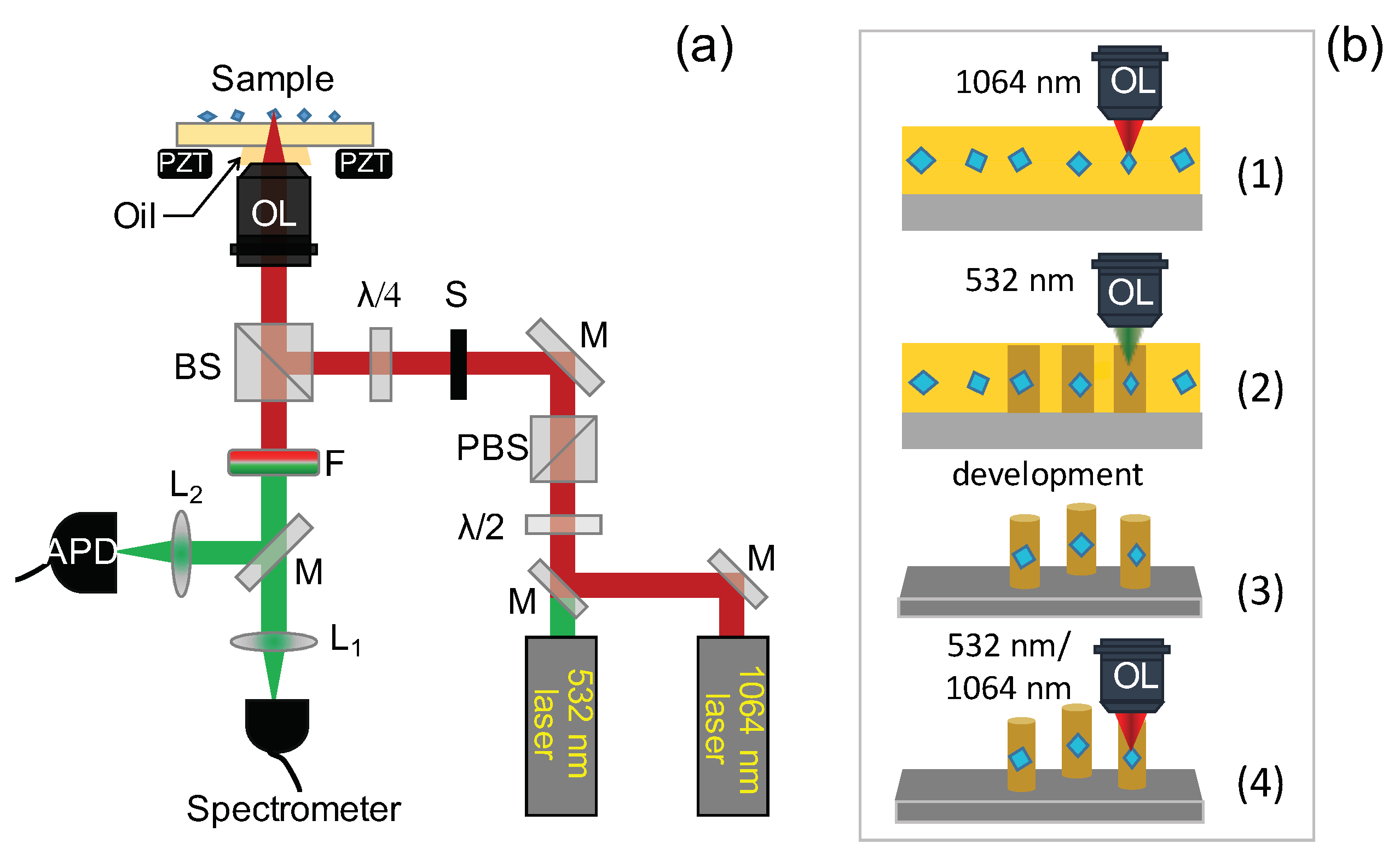
We added a pulsed 1064 nm laser (1 ns, 24.5 kHz) into the LOPA DLW setup. This laser allowed us to investigate the SHG signal of KTP NPs, before and after coupling to the photonic structure. This infrared laser is aligned with the 532 nm laser before being focused into the sample (see Figure 1a). The system can work with the 1064 nm laser or with the 532 nm laser by switching the mirror M1. Another half-wave plate for 1064 nm–wavelength was inserted after the PBS to adjust the polarization of the fundamental laser. To measure the SH signal (532 nm), a KG5 filter is used to cut off the fundamental beam (1064 nm). The SH signal was detected by either the APD to produce a SH image, or by a spectrometer to obtain a SH spectrum. This flexible setup allows both fabrication of desired structure containing a single KTP NP at LOPA regime and characterization of SHG enhancement. The whole process is illustrated in Figure 1b.
2.2. Shg Experimental Setup
In order to measure and to characterize the SHG signal of KTP NPs, we added a pulsed 1064 nm laser (pulse duration of 1 ns and repetition rate of 24.5 kHz) into the LOPA DLW setup. This second laser is aligned so that the laser beam coincides with that of the 532 nm laser (see Figure 1a). A flip-flop mirror allows us to switch easily from one laser to the other. A half-wave plate (not shown in the Figure) for 1064 wavelength can be placed after the polarizer to control the polarization of the fundamental laser beam. To collect SHG signal at 532 nm, an infrared filter is used to cut off the fundamental light at 1064 nm. The signal is then detected by either the APD which gives a SHG image, or a spectrometer which gives a SHG spectrum of the KTP NPs. This home-built setup is very flexible for signal detection as well as structure fabrication at LOPA regime, as illustrated in Figure 1b.
2.3. Ktp Nps Preparation
KTP NPs were obtained from KTP powders, which were extracted from the polishing process of a bulk KTP crystal. The synthesis process of KTP NPs can be described as follows [2]: The KTP powders were first mixed with a polyvinylpyrrolidone polymer (PVP) using a propanol solvent (PrOH) at a controlled concentration. The solution is then placed in an ultrasonic bath for 20 min in order separate KTP NPs assembly and to create a thin layer of PVP polymer around them, which then avoiding the particles aggregation. To obtain particles with a uniform size, the solution was first passed through a filter having a hole diameter of m, in order to eliminate big particles, and then centrifuged with a typical speed of 11,000 rpm for 15 min. This allowed obtaining a quasi-monodisperse solution with particles size between 30 and 100 nm. We dispersed these particles again in the 0.1% PVP/PrOH mixture, which was again placed in an ultrasonic bath to obtain the final colloidal KTP solution.
2.4. Sample Preparation and Fabrication Process
To obtain a monolayer of individual KTP NPs for SHG characterization or for fabrication, we mixed the colloidal KTP solution with ethanol with a solution/ethanol ratio of 1:5 using ultrasonication for 30 min. The solution was then spin-coated on a clean glass substrate (for SHG characterization) or on photoresist thin films (for coupling), resulting in a monolayer of well separated KTP NPs.
For fabrication of coupled structures, the photoresist sample was prepared as following. First, a thin layer (500 nm or 5000 nm) of SU8 was spin-coated on a cleaned cover glass. Then, a well dispersed KTP NPs solution was spin-coated on the surface of the first SU8 layer. Finally, a second thin layer (500 nm) of SU8 was deposited on top of the KTP NPs monolayer. To remove the solvents, the sample was placed on a hot plate at C for 3 min and at C for 5 min. We note that SU8 2000.5 photoresist was used to obtain a film of 500 nm thickness and SU8 2005 photoresist for a film of 5000 nm thickness. The choice of each thickness depends on the desired structures, 2D or 3D.
The fabrication of photonic structures containing a single KTP NP is shown in Figure 1b and consists of two main steps:
- -
- Determination of the position of a single KTP NP by detecting SHG signal using a pulsed 1064 nm laser.
- -
- Fabrication of the polymeric structure containing a single NP by LOPA-based DLW using a cw 532 nm laser.
We note that the two lasers have been perfectly aligned before the OL so that their focusing spots have the same transverse position, i.e., x and y coordinates. However, these spots are slightly different along the axial axis, due to the difference in wavelength. Practically, this was overcome by adjusting the z position in between the mapping (by 1064 nm laser) and the fabrication (by 532 nm laser) programs. After developing the sample to wash away all un-exposed photoresist, the fabricated structures were then placed again on the LOPA system in order to characterize the SH signal of KTP NPs and to compare it with that obtained before fabrication.
2.5. SHG of a Single KTP NP
We first characterized the SHG of individual KTP NPs spin-coated on glass substrate, by using the 1064 nm laser with a typical average laser power of 0.3 mW. The SH signal is very intense with respect to background noise (signal-to-background ratio of about 100), and a SHG image of an individual KTP NP is shown in Figure 2a. The intensity profile in the x-direction (Figure 2b) shows a full width at half maximum (FWHM) of approximately 500 nm, which agrees with the diffraction limit of the focusing spot at the 1064 nm wavelength (numerical calculation is about 480 nm). This allowed us to identify an individual KTP NP with a great precision. Figure 2c shows the spectral analysis of the SHG of a single KTP NP, obtained by adding an infrared filter to cut off the fundamental wavelength. A clear peak at 532 nm confirms the SHG of the 1064 nm laser. Figure 2d shows the temporal tracking of the SH signal. It shows a perfect stability of the SH signal for a long duration. The small variation of the SH signal is probably due to the mechanical instability of the optical setup. This excellent SHG stability allows us to optically address the same KTP NP at different moments, separated by several months, and to perform different types of measurements.
3. Deterministic Coupling of a Single KTP Particle into a Polymeric Structure
In order to fabricate a desired photonic structure containing a single KTP NP, we first determined the position of a KTP NP by scanning the sample with the 1064 nm laser as explained above. Experimentally, the position of a KTP NP was determined with a precision of about 10 nm. Then, the fabrication of desired polymeric structures containing the NP with well-known position was realized. For fabrications, the 1064 nm laser was off and the cw 532 nm laser was turned on. We demonstrated that the modified LOPA-based DLW technique allowed a full control of the coupling of a single KTP NP and an arbitrary polymeric structure.
3.1. Control of Shape of Structures
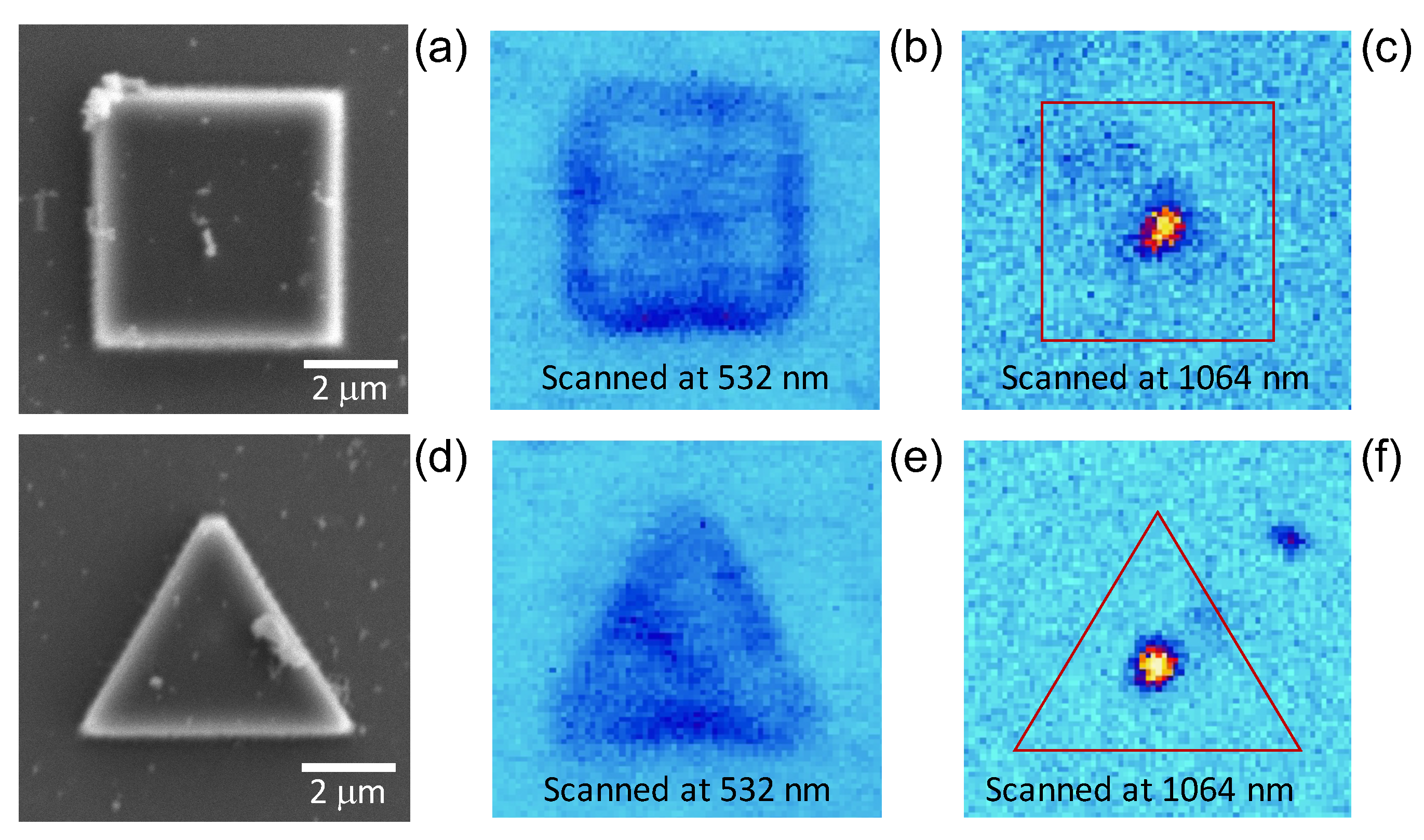
We first investigated the introduction of KTP NPs to structures having different shapes. Figure 3a,d show scanning electron microscope (SEM) images (top view) of a square and a triangular structures, fabricated by a laser power of 9 mW and a writing velocity of 3 m/s. These structures were fabricated by scanning the laser spot through the SU8 film, point by point to form square/triangular structures. The distance between two adjacent points was set at 150 nm, which is smaller than the diffraction limit, resulted in continuous photoresist lines/films. Figure 3b,e show the fluorescence images of the square and triangular shapes, respectively, obtained by 532 nm laser scanning (P = 50 W). Figure 3c,f represent the SHG images obtained by scanning with the 1064 nm pulsed laser. A bright spot at the center of the structure corresponds to the SHG signal emitted by the KTP NP.
The first conclusion is that the LOPA-DLW allowed us to realize any structure on demand containing a single nonlinear NP. Secondly, as compared to metallic NPs [18], the nonlinear NPs do not induce a thermal effect, which may influence the structure size and shape. This is an excellent advantage which can be further exploited to embed this KTP NP to different kinds of polymeric structure.
3.2. Control of NP Position in Polymeric Structures
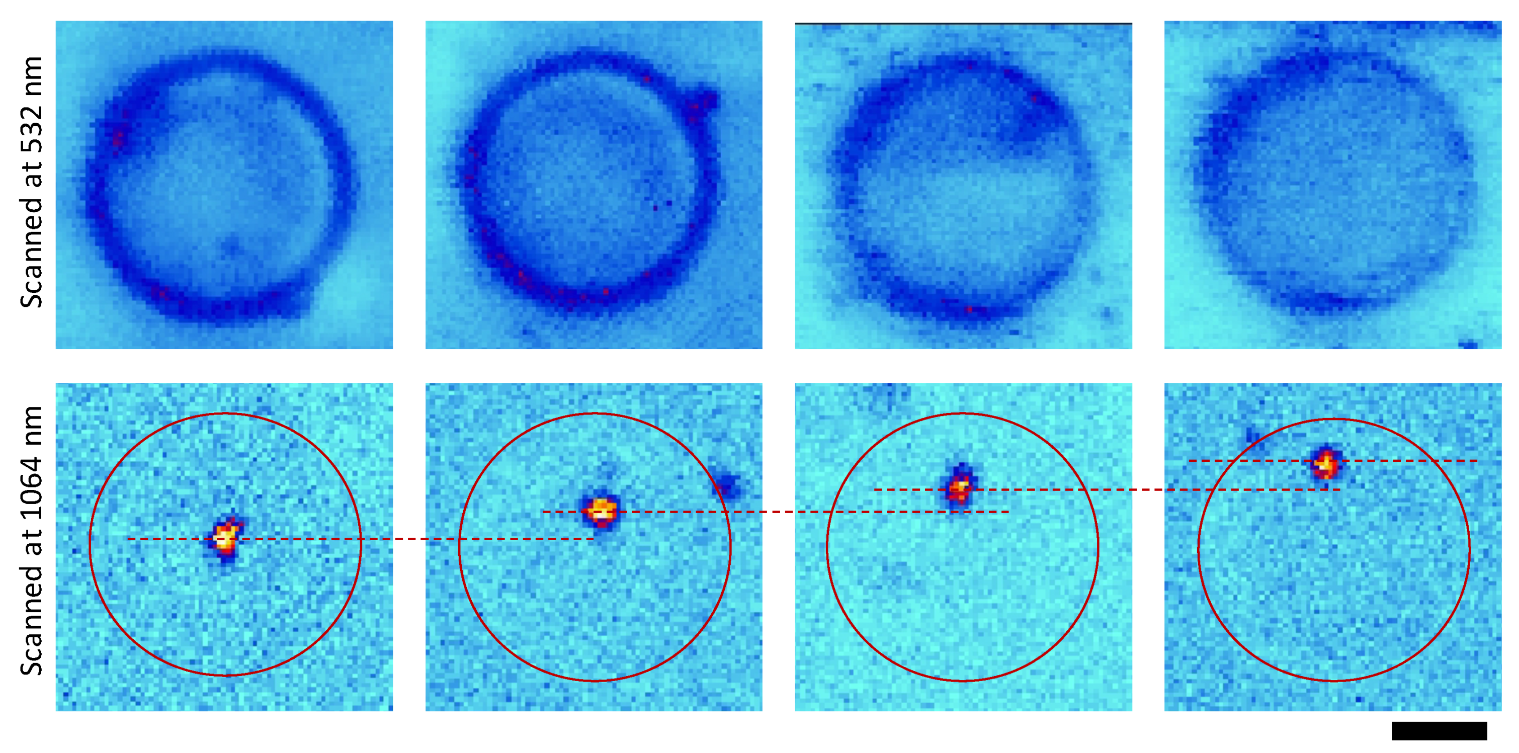
The control of position of the KTP NP in photonic structures is very importance, because the light intensity is usually not uniform in a resonant photonic structure. We therefore also demonstrated that LOPA based DLW allowed precisely controlling and manipulating the NP position in any polymeric structures. Several polymeric structures (e.g., triangle and circular disk) containing KTP NPs at different positions have been fabricated. Figure 4 shows fluorescence and SHG images of a series of polymeric microdisks embedding KTP NPs at different positions, from center to edge. The KTP NP position was experimentally controlled with a precision of 10 nm, that is mainly due to the diffraction limit of the optical system.
3.3. Control of Structure Size
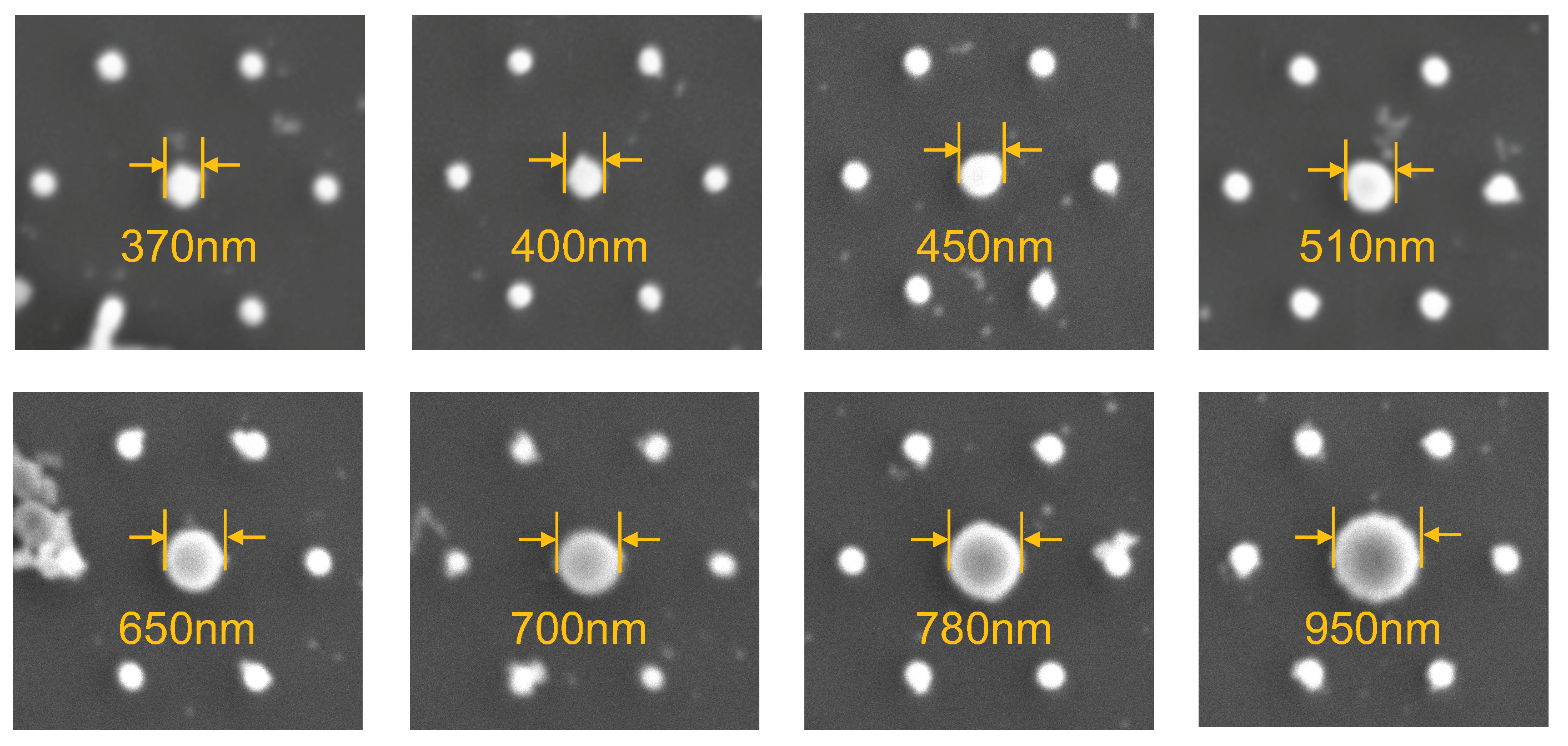
It was also demonstrated that by controlling the exposure dose, the size of the structure containing single KTP NPs is adjusted on demand. We fabricated various two-dimensional (2D) structures consisting of individual pillars among them the central one contains a single NP. Each pillar was fabricated by scanning the laser spot along the z–axis and through the photoresist film thickness (total scanning distance of 2 m). Figure 5 shows the SEM images of fabricated structures. All pillars were fabricated with the same exposure dose (P = 6 mW, v = 5 m/s), except the central one containing the KTP NP. For that, the doses were adjusted as: (top row) P = 6 mW, v = 4 m/s; 3 m/s; 2 m/s; v = 1 m/s; (bottom row) P = 9 mW, v= 4 m/s; 3 m/s; 2 m/s; and 1 m/s, respectively. In this example, the diameter of the central pillars increases with a step of about 50 nm. This can be controlled with a smaller step by finely controlling the laser power or the scanning speed, thanks to the non-explosion effect of the KTP NP in LOPA regime.
Thus, the second conclusion is that the LOPA DLW is a powerful technique to embed a single nonlinear NP into any PS with controlled size and shape, without any thermal effect. The position of the NP is also adjusted on demand inside the polymeric structures, which is a great advantage for photonic coupling.
3.4. Coupling of KTP NP to 3D Structures
Furthermore, we demonstrated that LOPA DLW enables the fabrication of three-dimensional (3D) structures containing a single KTP NP. For that, we used SU8 2005 (5 m–thickness) as the structure material. Figure 6a shows the SEM image of a hexagonal air-hole membrane containing a KTP NP at the center. To support the membrane, six polymeric legs were fabricated as shown in the inset of the Figure 6a. The membrane was fabricated (laser power of 10 mW; scanning speed of 3 m/s) by scanning the laser spot in a -plane with some missing exposures in a hexagonal configuration. Figure 6b,c show the fluorescence and SHG images of the center part of the membrane. The bright SHG spot confirms the presence of the KTP NP in the 3D membrane structure. It is worth mentionning that it is more challenging for fabrication of 3D structures containing NPs as compared to the case of 2D structures, because the 3D structure is thicker and therefore it is more difficult to find out the position of the NPs. For this moment, we didn’t find any SHG enhancement of the coupled KTP NP. This is due to the fact that the refractive index of the SU8 material is low and the periodicity of the 3D photonic membrane is not optimized to open a photonic bandgap, which is important to have a photonic coupling. This requires a long investigation and is out of the scope of this paper. However, the success of embedding a KTP NP into a 3D photonic structure is very encourageable, which suggests further investigations for fascinating applications.
4. SHG Signal Enhancement
In this section, as a demonstration of the coupling, we present our experimental investigation on the enhancement of the SH signal of a single KTP NP embedded in a polymeric submicropillar. This is further confirmed by a simulation model based on the FDTD method.
4.1. Experimental Measurement
In order to demonstrate the coupling effect of the fabricated structure, we have compared the SH signal of the same KTP NP obtained before and after being inserted into a polymeric pillar. The comparison was done by using the same experimental conditions, such as excitation power and measurement time.
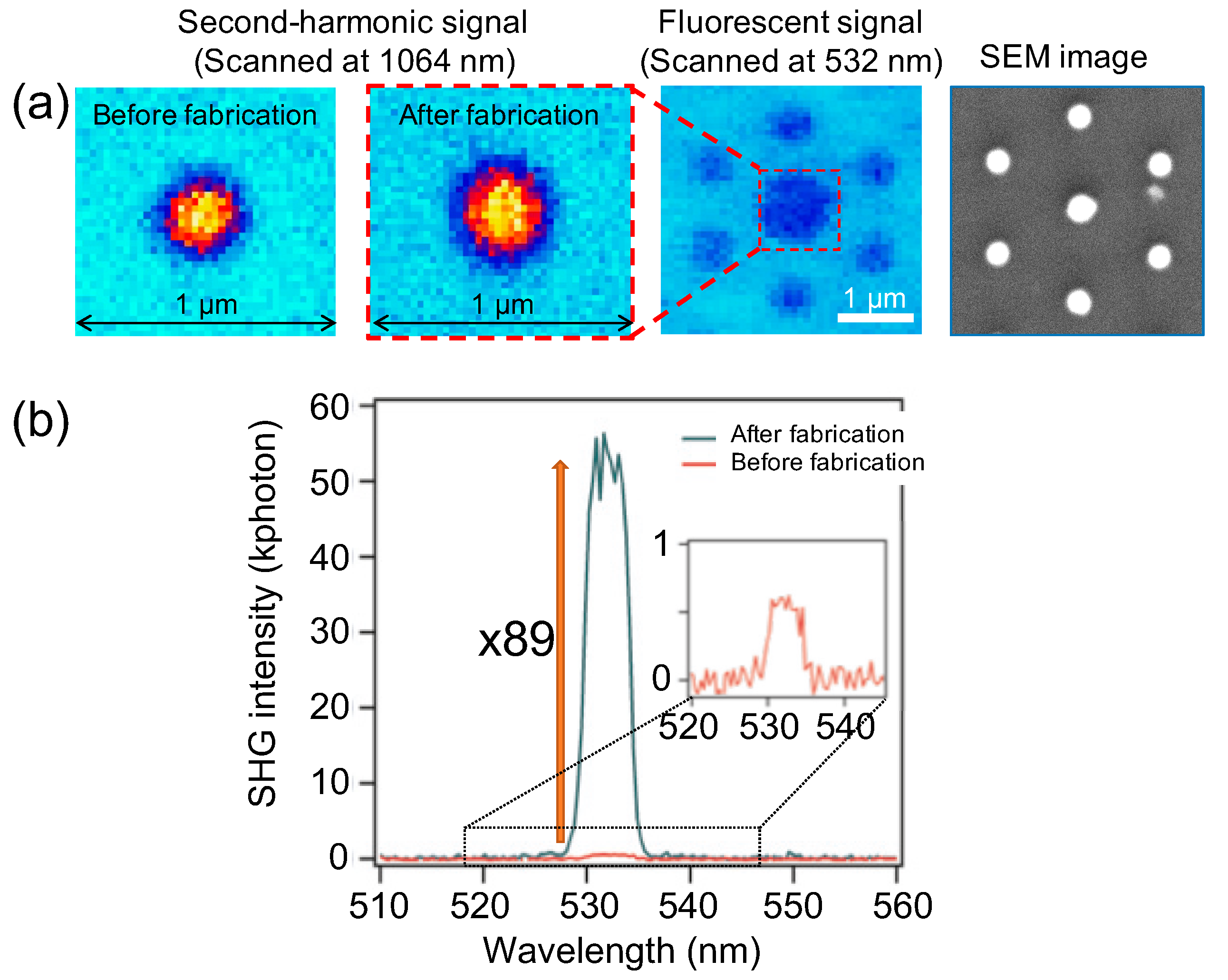
Figure 7a shows the SH images (by a pulsed 1064 nm laser) of a single KTP NP obtained before (with polymeric film) and after fabrication (with polymeric pillar), and a fluorescence image (by a cw 532 nm laser) of the fabricated structure. It can be seen from the images that the NP exists well inside the micropillar. We note that SU8 does not emit fluorescent or SH signal when excited by 1064 nm laser, therefore only the SH signal of the KTP NP was detected. Comparing the SH signal obtained before and after fabrication, we can clearly see a great enhancement. Figure 7b shows the comparison of the SHG intensities of the same KTP NP located in a polymeric film (red curve) and in a polymeric pillar (green curve). When embedded in a pillar (diameter = 800 nm; height = 1.3 m), the SHG intensity is enhanced up to 90 times. We have also realized many similar structures with the same fabrication parameters but containing different KTP NPs to verify the orientation dependence of the KTP NP inside the polymeric pillar. Indeed, while a bulk KTP crystal has a unique and well-defined orientation, a KTP NP is randomly oriented in space. This first affects the nonlinear interaction between the fundamental light and the nonlinear crystal, which depends strongly on the relative angle between the electric field of the fundamental beam and the main axis of the KTP crystal. Also, the amount of SH light collected by the microscope objective strongly depends on the orientation of the SH dipole and the surrounding medium. The detected SH signal is therefore the result of the photons number emitted by the nonlinear dipole and the collection efficiency of the optical system, which is defined as the ratio of the photons collected by the microscope to the total photons emitted by the dipole. Clearly, the polymeric pillar strongly enhanced the SHG emission towards the detection system thus enhancing the detected SHG signal. But the enhancement value varied from this NP to the other due to the random orientation of the KTP NP inside the pillar cavity.
4.2. Numerical Simulations
We have then performed different simulations using FDTD method to find out the answers for different questions: How the polymeric pillar cavity enhanced the incident fundamental light (at 1064 nm); How the polymeric pillar guided out the SH signal (at 532 nm) emitted from the embedded NP, and if the coupling out is affected by the NP’s orientation. For these simulations, we assumed that the SH signal is emitted from an electric dipole.
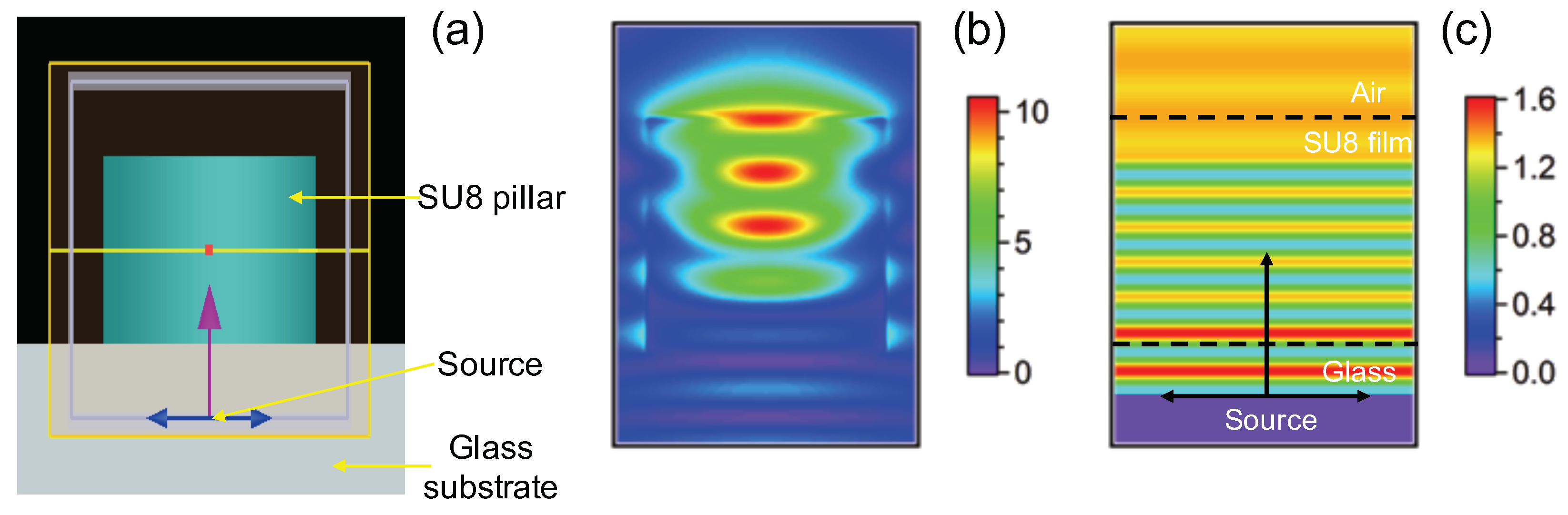
We first investigated the enhancement of the fundamental light in the polymeric pillar cavity. Figure 8a shows a model used for simulation. The polymeric pillar cavity was placed on a glass substrate and a plane-wave light source was inserted inside the glass substrate, which emits a 1064 nm–wavelength in upward direction (z-axis). This incident light field was monitored in the ()– or ()–plane. Similar simulations were also realized for a thin SU8 film deposited on a glass substrate to verify the field enhancement in polymeric cavity. The cavity parameters such as diameter and height are swept in a large range to find out the optimum configuration of the cavity. We found that the pillar possessing parameters similar to experimental structures induces a strong enhancement of the fundamental light. Figure 8b shows the intensity of the fundamental light inside a polymeric pillar with a diameter of 800 nm and a height of 1.3 m. Figure 8c shows the field intensity when the 1064 nm light passed though a thin film with a thickness of 1.3 m. It is clear that, the fundamental field is amplified and localized inside the pillar cavity, resulting in an amplification of 7 to 13 times, as compared to that inside the thin film. Therefore, when a KTP NP is embedded inside the polymeric pillar, the SHG will be enhanced by a factor in between 49 and 169. Furthermore, it was observed that a small change of NP position inside the cavity leads to a significant change of the SHG signal due to the modulation of the fundamental light field inside the cavity, as seen in Figure 8b. This suggests that the experimental determination of the NP position in the structures is very importance to obtain an optimum SHG enhancement.
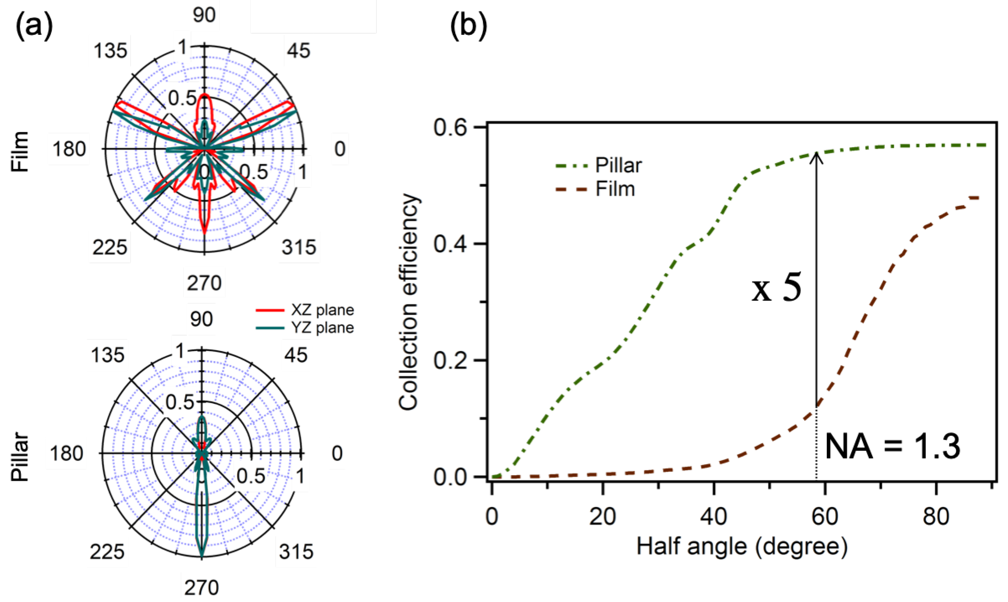
We then investigated how the SH light is coupled out of the cavity. For simplification, we considered the nonlinear NP as a single oscillating electric dipole. Naturally, we found that the best orientation of the emitting dipole should be parallel to the glass substrate surface. We have then compared the two particular configurations: a single KTP NP embedded in a polymeric film (thickness = 1.3 m) and a polymeric pillar (diameter = 800 nm; height = 1.3 m). Furthermore, the emitting dipole is assumed to be embedded in polymeric material at center of the thin film or of the pillar, i.e., at 650 nm from the glass interface. The SHG detector is placed inside the glass substrate. Figure 9a shows the SH intensity distribution in the () and ()–planes of a single emitting dipole embedded in a polymeric film (top) and in a polymeric pillar (bottom). It is evident that, thanks to the pillar cavity, the emitted light is compressed in a small cone and mostly directed towards the detector (downward direction). In contrast, in the case of the film, the light is generated in a large angle, which cannot be totally detected by the detector. To be more precise, we have numerically evaluated the collection efficiency of the emitted light as a function of the microscope objective, a main component of the detection system. Figure 9b shows the simulation result of the collection efficiency as a function of the half angle, defined as arcsin(NA/n), where NA is the numerical aperture of the objective lens and n is the refractive index of the immersion oil. In case of an objective lens with NA = 1.3 (half angle = ), 55% of the photons emitted by the NP embedded in a polymeric pillar can be collected while this is only 11% in the case of polymeric film. The polymeric pillar cavity thus does not only amplify the fundamental light intensity, resulting in an enhancement of the nonlinear optical process, but also guide the emitted signal into the detection angle, hence enhancing the collection efficiency. Theoretically, when the KTP NP is embedded at the middle of the pillar, the best collection efficiency is obtained with a pillar having a diameter of 800 nm and a height of 1300 nm, which is quite consistent with the experimental result.
5. Conclusions
In this work, we have first investigated the SHG of individual KTP NP with a size of about 100 nm, under a pulsed laser excitation at 1064 nm. The KTP NP shows a high nonlinear coefficient, as compared to a bulk one, and the SHG is perfectly stable at room temperature. Its transparency for both wavelengths of the fundamental and SH wavelengths leads to a high signal to noise ratio. We then demonstrated the LOPA-based DLW as an excellent technique to realize desired polymeric photonic structures containing a single KTP NP. Thanks to its transparency at 532 nm, KTP NPs did not induce explosion or damage during fabrication. Different kinds of 2D and 3D polymeric structures containing individual KTP NPs were successfully demonstrated. The size and shape of the polymeric structures and the position of the KTP NP inside the structure were demonstrated to be controlled at nanoscale. When the KTP NP is embedded in a polymeric pillar, the SHG is enhanced by a factor of 90. The SHG enhancement was varied for different KTP NPs, because of the random orientation of the NP inside the cavity. This affects the nonlinear interaction between the fundamental beam and the KTP crystal as well as the collection efficiency of the optical system. Different simulations using FDTD method have been done and shown very good agreement with the experimental results.
Author Contributions
D.T.T.N. and N.D.L. conceived and designed the experiments; D.T.T.N. performed the experiments, analyzed the data, and did simulations. All authors wrote, reviewed and approved the final version of manuscript.
Funding
This research is funded by a public grant overseen by the French National Research Agency in the frame of GRATEOM project (ANR-17-CE09-0047-01).
Acknowledgments
We thank L. Le Xuan and J.-F. Roch for providing nonlinear nanoparticles, I. Ledoux-Rak for fruitful discussion about nonlinear optics, and Phoebe Marcus-Porter for English revision.
Conflicts of Interest
The authors declare no conflict of interest.
References
- Boyd, R. Nonlinear Optics, 3rd ed.; Academic Press: Cambridge, MA, USA, 2008; pp. 1–640. [Google Scholar]
- Le Xuan, L.; Zhou, C.; Slablab, S.; Chauvat, D.; Tard, C.; Perruchas, S.; Gacoin, T.; Villeval, P.; Roch, J.-F. Photostable Second-Harmonic Generation from a Single KTiOPO4 Nanocrystal for Nonlinear Microscopy. Small 2008, 4, 1332–1336. [Google Scholar] [CrossRef] [PubMed]
- Zielinski, M.; Oron, D.; Chauvat, D.; Zyss, J. Second-Harmonic Generation from a Single Core-Shell Quantum Dot. Small 2009, 5, 2835–2840. [Google Scholar] [CrossRef] [PubMed]
- Gao, X.; Cui, Y.; Levenson, R.-M.; Chung, L.-W.; Nie, S. In vivo cancer targeting and imaging with semiconductor quantum dots. Nat. Biotechnol. 2004, 22, 969–976. [Google Scholar] [CrossRef] [PubMed]
- Kachynski, A.V.; Kuzmin, A.N.; Nyk, M.; Roy, I.; Prasad, P.N. Zinc Oxide Nanocrystals for Nonresonant Nonlinear Optical Microscopy in Biology and Medicine. J. Phys. Chem. C 2008, 112, 10721–10724. [Google Scholar] [CrossRef] [PubMed] [Green Version]
- Extermann, J.; Bonacina, L.; Cuna, E.; Kasparian, C.; Mugnier, Y.; Feurer, T.; Wolf, J.-P. Nanodoublers as deep imaging markers for multi-photon microscopy. Opt. Express 2009, 17, 15342–15349. [Google Scholar] [CrossRef] [PubMed]
- Grange, R.; Lanvin, T.; Hsieh, C.-L.; Pu, Y.; Psaltis, D. Imaging with second-harmonic radiation probes in living tissue. Biomed. Opt. Express 2011, 2, 2532–2539. [Google Scholar] [CrossRef] [PubMed] [Green Version]
- Staedler, D.; Magouroux, T.; Hadji, R.; Joulaud, C.; Extermann, J.; Schwung, S.; Passemard, S.; Kasparian, C.; Clarke, G.; Gerrmann, M.; et al. Harmonic Nanocrystals for Biolabeling: A Survey of Optical Properties and Biocompatibility. ACS Nano 2012, 6, 2542–2549. [Google Scholar] [CrossRef] [PubMed]
- Ibanez, A.; Maximov, S.; Guiu, A.; Chaillout, C.; Baldeck, P.L. Controlled Nanocrystallization of Organic Molecules in Sol-Gel Glasses. Adv. Mater. 1998, 10, 1540–1543. [Google Scholar] [CrossRef]
- Sanz, N.; Baldeck, P.L.; Nicoud, J.-F.; Le Fur, Y.; Ibanez, A. Polymorphism and luminescence properties of CMONS organic crystals: Bulk crystals and nanocrystals confined in gel-glasses. Solid State Sci. 2001, 3, 867–875. [Google Scholar] [CrossRef]
- Treussart, F.; Botzung-Appert, E.; Ha-Duong, N.-T.; Ibanez, A.; Roch, J.-F.; Pansu, R. Second Harmonic Generation and Fluorescence of CMONS Dye Nanocrystals Grown in a Sol-Gel Thin Film. ChemPhysChem 2003, 4, 757–760. [Google Scholar] [CrossRef] [PubMed]
- Delahaye, E.; Tancrez, N.; Yi, T.; Ledoux, I.; Zyss, J.; Brasselet, S.; Clement, R. Second harmonic generation from individual hybrid MnPS3-based nanoparticles investigated by nonlinear microscopy. Chem. Phys. Lett. 2006, 429, 533–537. [Google Scholar] [CrossRef]
- Driscoll, T.A.; Hoffman, H.J.; Stone, R.E.; Perkins, P.E. Efficient second-harmonic generation in KTP crystals. J. Opt. Soc. Am. B 1986, 3, 683–686. [Google Scholar] [CrossRef]
- Hohmann, J.K.; Renner, M.; Waller, E.H.; von Freymann, G. Three- Dimensional μ-Printing: An Enabling Technology. Adv. Opt. Mater. 2015, 3, 1488–1507. [Google Scholar] [CrossRef]
- Maruo, S.; Fourkas, J. Recent progress in multiphoton microfabrication. Laser Photonics Rev. 2008, 2, 100–111. [Google Scholar] [CrossRef]
- Li, Q.; Do, M.T.; Ledoux-Rak, I.; Lai, N.D. Concept for three-dimensional optical addressing by ultralow one-photon absorption method. Opt. Lett. 2013, 38, 4640–4643. [Google Scholar] [CrossRef] [PubMed]
- Do, M.T.; Nguyen, T.T.N.; Li, Q.; Benisty, H.; Ledoux-Rak, I.; Lai, N.D. Submicrometer 3d structures fabrication enabled by one-photon absorption direct laser writing. Opt. Express 2013, 21, 20964–20969. [Google Scholar] [CrossRef] [PubMed]
- Do, M.T.; Nguyen, D.T.T.; Ngo, H.M.; Ledoux-Rak, I.; Lai, N.D. Controlled coupling of a single nanoparticle in polymeric microstructure by low one-photon absorption–based direct laser writing technique. Nanotechnology 2015, 26, 105301. [Google Scholar] [CrossRef] [PubMed]
Figure 1.
(a) Experimental setup of the integrated optical system for fabrication of desired polymeric structures and for characterization of SHG of a single KTP NP. PZT: piezoelectric translator, OL: oil immersion microscope objective, /4: quarter-wave plate, /2: half-wave plate, BS: unpolarizing beam splitter, PBS: polarizing beam splitter, M: mirrors, S: electronic shutter, : lenses, F: infrared filter, APD: avalanche photodiode. (b) Fabrication process of polymeric structures containing single KTP NPs. (1) Identification of KTP NPs positions by 1064 nm laser (SHG mapping); (2) Fabrication of photonic structures containing single KTP NP by 532 nm laser; (3) Development of samples; (4) Characterization (SHG by 1064 nm laser or fluorescence by 532 nm laser) of coupled structure.

Figure 2.
(a) Second-harmonic image of a KTP NP with a size of about 100 nm, obtained by scanning with a pulsed 1064 nm laser. (b) The SHG intensity profile in the x-direction, extracted from (a), showing a FWHM of 500 nm. (c) SHG spectrum. (d) Time evolution of the SHG signal obtained by an average power of 0.3 mW. The signal is stable for a long duration.

Figure 3.
(a) SEM image of a square structure containing a KTP NP at the center. Fluorescence image (b) and SHG image (c) of the corresponding structure, obtained by scanning with 532 nm laser and 1064 nm laser, respectively. The SHG image shows clearly that the polymeric square structure contains a KTP NP at the center. (d–f): similar SEM, fluorescence et SHG images of a triangular structure containing a KTP NP.

Figure 4.
Top row: Fluorescence images of microdisk structures, obtained by scanning with a 532 nm cw laser. Bottom row: SH images of corresponding structures obtained by scanning with 1064 nm laser. The bright spots correspond to the SHG of KTP NPs, which are embedded at different positions of the microdisk, from center to edge. Scale bars: 1 m.

Figure 5.
SEM images of pillars structures containing single KTP NPs. All pillars were fabricated by the same exposure dose, except the central one, which was fabricated by the following parameters. Top row: from left to right: P = 6 mW, m/s; m/s; m/s; and m/s, respectively. Bottom row: from left to right: P = 9 mW, m/s; m/s; m/s; and m/s, respectively.

Figure 6.
3D hexagonal membrane structure containing a KTP NP. (a) SEM image; Inset: full side view. (b) Fluorescence image obtained by scanning with a 532 nm laser with low power. (c) SHG image, obtained by scanning with 1064 nm laser, showing the existence of a KTP NP at at center of structure.
Figure 6.
3D hexagonal membrane structure containing a KTP NP. (a) SEM image; Inset: full side view. (b) Fluorescence image obtained by scanning with a 532 nm laser with low power. (c) SHG image, obtained by scanning with 1064 nm laser, showing the existence of a KTP NP at at center of structure.

Figure 7.
(a) SHG images of a KTP NP obtained before and after fabrication, and a fluorescence image of the fabricated structure. In the right: SEM of corresponding fabricated structure. (b) Comparison of the SHG spectra intensities of the same KTP NP showing an enhancement factor of about 90; Inset: zoom-in of the SHG spectrum before fabrication.

Figure 8.
(a) Illustration of the model used to simulate the coupling of a light beam and a polymeric pillar. A light beam at 1064 nm–wavelength is emitted from the source and sent towards the cavity (, ). (b) Simulation of light intensity inside a polymeric pillar (diameter = 800 nm, height = m). (c) Simulation of light intensity at 1064 nm–wavelength propagating through a polymeric film (thickness = m).

Figure 9.
(a) Simulation of radiation patterns, in () and ()–plane, of a single dipole embedded in different configurations. Top: emission diagram of a single dipole embedded in a thin film. Bottom: emission diagram of a single dipole embedded in a polymeric pillar. For both cases, the dipole was assumed to be in x-axis. (b) Calculation of the collection efficiency of the SHG signal as a function of the half angle of the objective lens for two cases. An enhancement factor of 5 is obtained.

© 2019 by the authors. Licensee MDPI, Basel, Switzerland. This article is an open access article distributed under the terms and conditions of the Creative Commons Attribution (CC BY) license (http://creativecommons.org/licenses/by/4.0/).
Share and Cite
MDPI and ACS Style
Nguyen, D.T.T.; Lai, N.D. Deterministic Insertion of KTP Nanoparticles into Polymeric Structures for Efficient Second-Harmonic Generation. Crystals 2019, 9, 365. https://0-doi-org.brum.beds.ac.uk/10.3390/cryst9070365
AMA Style
Nguyen DTT, Lai ND. Deterministic Insertion of KTP Nanoparticles into Polymeric Structures for Efficient Second-Harmonic Generation. Crystals. 2019; 9(7):365. https://0-doi-org.brum.beds.ac.uk/10.3390/cryst9070365
Chicago/Turabian StyleNguyen, Dam Thuy Trang, and Ngoc Diep Lai. 2019. "Deterministic Insertion of KTP Nanoparticles into Polymeric Structures for Efficient Second-Harmonic Generation" Crystals 9, no. 7: 365. https://0-doi-org.brum.beds.ac.uk/10.3390/cryst9070365
Note that from the first issue of 2016, this journal uses article numbers instead of page numbers. See further details here.