1. Introduction
Scintillating crystal-based detectors are the main devices used for radiation and particle detection. The scintillating substances, by converting radiation into visible light, produce the main signal, which is then acquired by photoelectric sensors and analyzed by electronic and computing devices. Thanks to this capability, they are key components in a variety of measurement systems and diagnostic machines and are relevant in a number of scientific and technical areas whose impact on society is great: medicine, aerospace, security, and high-energy physics are some of the fields in which scintillators are involved [
1,
2]. These challenging environments are continuously pushing research and industry towards better-performing systems in order to meet the increasingly demanding requirements of their fields [
3,
4]. Medical devices for cancer diagnosis and treatment as well as for nuclear imaging (PET, SPECT, and CT scanner systems) require spatial resolution, accuracy, and fast response in order to achieve efficient diagnosis and treatment of patients at a reduced cost and time of exposure. The 10 ps coincidence time resolution (CTR) challenge for PET systems aims to produce a real-time, detailed medical imager for fast and minimally invasive procedures [
5,
6]. Environmental scanners need energy resolution and sensitivity in order to be able to discriminate the amount and type of radiation. Security systems must be fast and sensitive in order to reduce the dose and the time for an accurate inspection of the suspicious substances. Systems for aerospace and high-energy physics instruments need reliability, durability, and stability over a wide range of conditions and time. For example, calorimeter mechanical design imposes project specifications on the ultimate tensile strength and elastic properties of crystals [
7,
8]. Scintillators must withstand severe environmental demands in terms of temperature, mechanical stress, moisture, and radiation dose. Some examples are the high-luminosity LHC project and the new PANDA and Mu2e projects [
9,
10], in which the scintillating crystals must maintain light transport and collection for as long as possible under a severe radiation regime and uncontrollable environmental conditions. Scintillators are found in industry, exploited in detectors aimed at process and material testing, and in scientific devices too (e.g., X-ray diffractometers) which play a role in control, inspection, and investigation. Monocrystalline scintillators are still the most efficient and promising material to meet the new challenging requirements and future applications [
3]. Among them, anisotropic ones like PWO, LYSO, ZnWO, and LaBr are the most reliable and accurate [
11,
12].
The production process of such materials and their tailoring for different purposes are complex and expensive. These crystals are grown by basic two methods, Bridgman and Czochralsk; both involve high-temperature furnaces in which the raw materials are melted; subsequently, the melted substance is put in contact with a high-quality crystalline seed and slowly cooled. The control of atmosphere, gaseous pressure, temperature, and speed are critical in order to obtain stable crystal growth, in which the condition for the substance to organize itself into a monocrystalline structure with a homogeneous distribution of the possible dopants is met. The crystal “boule” (the unrefined bulk crystal) is then finished and worked according to the intended tasks; it is usually cut into different dimensions and geometries according to the detector system’s specification. Surface treatments and, possibly, special coatings can be applied in order to enhance the light transport and collection properties. Overall, crystal production is a multi-stage process for which process control and quality control play a fundamental role in preventing defects.
Although anisotropic crystals offer very high performance, they are very sensitive to stress, structural conditions, and defects [
13,
14]. Small changes in the production parameters or environmental conditions can create unwanted defects that dramatically affect the scintillating behavior, reducing the crystals performance and lifetime. Since they are brittle materials, the residual stress must be taken into account to prevent unwanted mechanical failures (even during the production process) and internal fractures that make those materials unusable [
15]. Structural macro-distortions, dispersion of inclusions and/or impurities, and dislocation distribution play a crucial role in the scintillator light production, transport, and collection. The collection of the visible photons produced by the scintillator is the signal transmitting information on the observed phenomena; therefore, the surface texture and condition are crucial in order to have a perfect match with the photosensor.
Quality control and monitoring of these features are fundamental at each level of the scintillating crystal’s life cycle: research, industry, production, and application. In most cases the quality control of these materials can be attained by visual inspection based on the experience of the production personnel, at the production stage, and by the measurements of the crystal’s scintillating and light performances at the end-user level.
The measurement methods presented in this work give detailed information about structural quality at different scales. Photoelasticity-based techniques [
16,
17] will be presented in the two different and complementary forms of laser conoscopy and sphenoscopy; these non-invasive techniques, and the associated theoretical models, allow us to collect information about residual stress, macro-defects and structural macro-distortion distribution, producing feedback for the tuning of the production parameters, ensuring the crystals’ correct light transport capability and predicting the functional behavior in a fast but reliable manner. These methods are particularly suitable for crystal producers, researchers, and end-users since they are non-destructive and all the samples of the production can be inspected.
As far as extremely detailed inspection and quality assessment methods are concerned, XRD, SEM, EDX, and TEM analytical methods will be surveyed. These techniques give information on the crystal lattice structure, compound distribution, and structural morphology at the micro- and nanometric scale. On the other hand, they require carefully prepared samples, they can be destructive techniques, and they are time consuming since they need special preparation of the sample and complex instrumentation. Finally, we will describe and review the grazing incident diffractometry (GID) method for surface roughness and crystallinity assessment. Some important information about crystals’ interfaces can be obtained by this last method. They allow the proper tuning of the finishing procedures aimed at achieving optimal light guidance and collection of the detector system. All these presented methods can be combined to arrive at a qualification procedure for the assessment of the crystals’ condition and the qualification of the production process.
2. Photoelasticity-Based Methods
Photoelasticity has been used for many decades for assessing the stress condition in isotropic and transparent materials like glass and Perspex; in some cases these materials are arranged in geometries similar to the mechanical and structural systems whose load-induced stress distribution have to be investigated [
7,
16,
17]. Photoelasticity can be implemented in several modes (e.g., transmission, reflection, and scattered modality); in all cases, photoelasticity generates fringe patterns that depend on the state of stress of the analyzed structure [
16,
17]. No fringes are generated in isotropic media if no stress or no refraction index variation are present into the volume. On the contrary, in anisotropic crystals, fringe patterns are present even in unstressed conditions due to their crystallographic structure. This led to more complex methodologies aimed at carrying out and analyzing the fringe patterns’ shape as a signature of defects and stress. In the following, we describe some recently developed methods that merge photoelasticity and optics for anisotropic crystal inspection.
2.1. Laser Conoscopy
2.1.1. Conoscopic Fringe Patterns and Their Interpretation
Conoscopy is an optical crystallographic technique that uses polarized light to acquire information about the crystalline materials and their optical characteristics. It is classically implemented in polarized microscopes for observing thinly sliced samples for mineralogy purposes [
18]. The technique has been adapted to measure residual stress in anisotropic crystals (a synonym for naturally birefringent crystals).
The crystal optical properties are described by the inverse permittivity or dielectric impermeability tensor
B, a second-order symmetric tensor whose principal components
Bx,
By, and
Bz are associated with the principal refractive indices
nx,
ny, and
nz by:
The tensor
B is associated to the optical indicatrix or index ellipsoid (
Figure 1a), whose equation is
which is a sphere for isotropic crystals (three equal refractive indices), a rotation ellipsoid (spheroid) for a uniaxial crystals (two equal refraction indices with one optic axis) or a general ellipsoid for biaxial crystals (three different refraction indices and two optic axis that are orthogonal to the planes that intersect the ellipsoid into a circumference). The light crossing the crystal’s volume is affected by the refraction indices; its velocity and polarization are changed as a function of the index ellipsoid (
Figure 1b) [
19,
20]. In a plane polariscope configuration, each polarized ray of light that impinges on the crystal surface is split and orthogonally polarized. They exhibit a phase delay and an interference pattern is obtained when they are recombined after the analyzer (
Figure 1b,c).
As an example, in
Figure 1c we show a typical interference image for a uniaxial crystal observed along its optic axis. The fringe orders are due to the optical path difference according to:
where
N is the fringe order (or the delay),
λ is the wavelength of the light,
no and
ne are the ordinary and extraordinary refractive index, respectively,
θ is the angle between the ray of light and the optic axis, and
d is the sample thickness. Equation (3) holds for uniaxial crystals; otherwise, in biaxial ones, the Fresnell law changes to:
where
ρ is the mean ray between the ordinary and the extraordinary one,
λ is the wavelength of the impinging light,
θ1,
θ2 are the angles formed by the ray and optic axes, respectively, and Δ the phase difference between the ordinary and extraordinary rays.
These patterns are due to the structure of the crystals and are based on the theory of the Bertin surfaces [
22,
23,
24] (Equation (2)), which are the virtual iso-delay surfaces that the light generates when crossing the sample (
Figure 1d,e). As a matter of fact, Bertin’s surfaces are the bijective relation between the light direction angle with the optic axes and a point in space and can be expressed as [
19,
20]:
Equation (5) is the general expression of the Bertin’s iso-delay surfaces in
Figure 1d,e. The angle
β is the angle between the optic axes and their bisector (the
z axis in
Figure 1e,d;
β = 0 in uniaxial crystals). The
β angle of the acute optic bisector (
OB) is given by:
The interferograms in
Figure 1c,f can be modeled as the intersection of the surfaces in
Figure 1d,e with a plane orthogonal to the
Z axis. Whenever a stress is applied on the crystal, the Bertin surfaces and, consequently, the fringe pattern deforms (
Figure 1e,f). The Bertin surface distortion depends on the fourth-order piezo-optic tensor
π, which depends on the crystal symmetries, as follows:
where
B0 is the dielectric impermeability tensor in unstressed condition; a detailed description of the related theory is given in [
25].
Due to the anisotropy, the generated patterns are a function of the observation direction with respect to the
OB (
Figure 1c,f and
Figure 2a,b).
In this paper, we concentrate on the two main directions in uniaxial crystals, but the method and the technique can be extended to biaxial ones. The fringe pattern obtained observing along the OB (optic axis in unstressed uniaxial crystals) deforms in case of stress. The circular fringe orders (in unstressed uniaxial crystals) alter into fourth-order Cassini Like (CL) curves that approximate ellipses for small stress. Measuring the major and minor axis of the elliptic first fringe order, the stress can be evaluated via
where
fσ is the photoelastic constant and
C is the ellipticity measured, referring to
Figure 1f, following the semi-phenomenological relation:
where Δ
X > Δ
Y always holds true in reference to Bertin surfaces (
Figure 1d,e) [
25].
Once the uniaxial crystal is stressed, it behaves like a biaxial crystal observed along the acute bisector of its optic axes, so the method can be extended to this latter category. In fact, Equation (9) is also valid for naturally birefringent crystals, taking into account that the unstressed interference pattern is composed of CL curves. For the analytical expression of the photoelastic constant and the ellipticity, refer to [
25,
26,
27]. By observing orthogonally to the optic axis (or along the obtuse bisector of biaxial crystals), the interferogram appears as a series of hyperbolas (
Figure 2a,b). In this case, the distance between the hyperbolas of the branches is linked to the stress condition by the following relation (Equation (10)), which is derived from a more complex model [
14]:
where
k0 is the difference
R in unstressed condition and
kσ is the photoelastic constant relevant to this direction.
If the piezo-optic tensor π elements are unknown, in both observation directions a calibration step is required in order to evaluate the photoelastic constants. Finally, these methods allow us to evaluate the internal stress state, which is linked to the whole crystal quality.
Interference and conoscopic methods are also useful to evaluate the piezo-optic surface, stress, and the
π tensor elements [
28,
29,
30]. That method is based on the difference between the radius vector in the optic indicatrix perturbed by stress and the unstressed one.
2.1.2. Implementation
Laser conoscopy is based on the plane/circular polariscope setup [
21,
31,
32]. Despite its reliability, the classical diffused light source has been substituted with a polarized laser source. In fact, diffused light polariscopes have limitations in terms of their spatial resolution, sensitivity, and complexity of analysis when used for anisotropic media. Since the sample is fully illuminated, the pattern carried out by the diffused light polariscope is due to the whole volume; therefore, complex shapes are obtained if the stress distribution is not uniform over the sample [
22]. Moreover, this full field technique has a limited sensitivity to local variations in the stress condition since they are averaged on the entire crystal volume [
32]. Collimated laser light with a special optical layout allows us to confine the light in a known portion of the crystal volume (
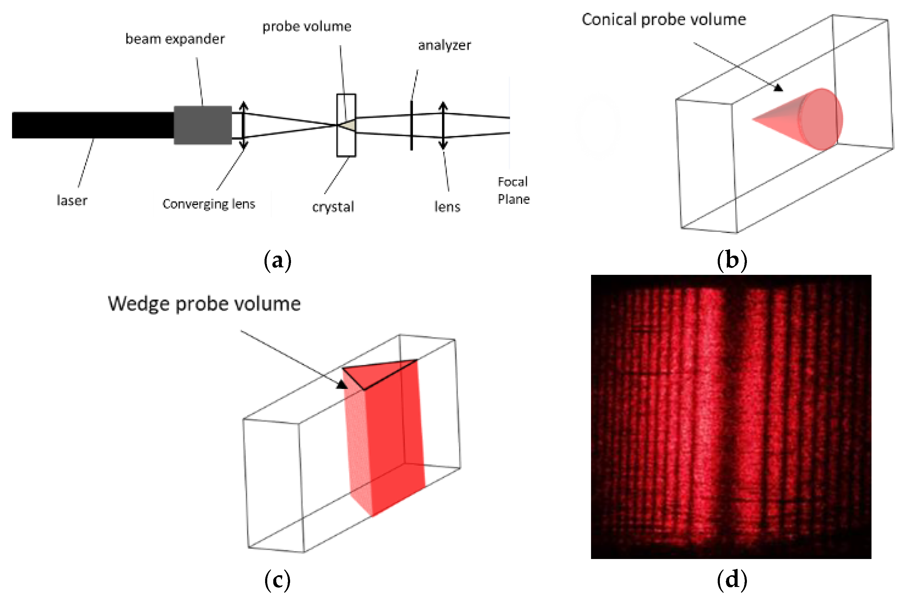
Figure 3a,b).
As the volume decreases, the sensitivity and spatial resolution increase. In the same manner, the complexity of the fringe pattern is reduced if a stress gradient or complex stress distribution is present over the crystal volume [
32]. Since the fringe pattern is generated solely by the illuminated volume, it is reasonable to consider the stress uniform if this volume is small. This leads to the generation of simple geometric shape of the fringes (circles, ellipses, or hyperbolas). The improved spatial resolution of this pointwise method is paid with the necessity of a scanning procedure to map the entire crystal sample in detail.
2.2. Sphenoscopy
Laser conoscopy provides details for each point of observation; however, the technique may require a large number of scanned points to cover an extended sample. Therefore, this procedure may not always be compatible with those scenarios that require a very short testing time (e.g., in line inspection of mass production systems). For this it is possible to introduce a new inspection layout, leading to the new concept of sphenoscopy [
33]. The scheme in
Figure 3a has been modified, substituting a cylindrical lens for the spherical one. Since the focus is a line instead of a point, the light volume generated in the crystal is a thin wedge (
Figure 3c). By this method an entire line is inspected, instead of a series of points, in one single acquisition. Consequently, the inspection procedure could be reduced from
acquisitions to
acquisitions. The sphenoscopic fringe pattern is simplified with respect to the conoscopic one; as with the Bertin model, the light spans over a plane angle only, so one dimension of the fringe orders is obtained. Different to the laser conoscopy, where the iso-delay surfaces are a bijective function of an angle that spans the three spatial dimensions, the sphenoscopy is due to the bijective relation between a plane angle and the space. The pattern is generated by the envelope of this dimension over the light wedge height, which lead to a fringe figure composed of a series of lines (
Figure 3d). The presence of defects, stress, or non-uniformities over the inspected volume modifies the lines’ curvature and the distances between them. The complexity of the pattern interpretation is, therefore, reduced. Even though the information gathered in this method is less than the conoscopic figures, the results are comparable. Sphenoscopic inspection remains suitable, for instance, for a fast control of conformity.
The methodologies detailed in this paragraph offer a set of possibilities to build a non-invasive and fast control system that is manageable and adaptable to different conditions and scenarios of inspection and monitoring.
Applicability of such methodologies spreads over the entire scintillating crystals value chain. The non-invasiveness and speed of the techniques are particularly useful at the production stage. The entire population of crystals can be inspected by photoelastic-based methods. This monitoring can be implemented at different stages of the process: for instance, soon after the growth, to implement growing process evaluation and decide on the best cutting procedure; before and after the machining process to assess the process itself, monitor possible defects, prevent unwanted failures, etc. An inspection of the incoming samples can be easily done by the end-user (such as detector producers and assemblers) to recognize and select samples with a low level of defectiveness. Research bodies have a powerful tool to study the link between structure, defectiveness, and performance of the scintillators. Stress structures, observed by photoelasticity, indicate macro-distortion of the lattices, which can be due to the production process and/or the presence of defects such as unwanted precipitates or clusters of particles that may affect the mechanical properties and the scintillation performances. In fact, the distribution of stress and defects influences the light transport and collection since the crystals can undergo lensing effects, generating unwanted focal points inside the structure and the modification of internal reflection conditions, and creating a preferential light path into the sample volume that can affect properties like decay time, energy resolution, and light yield. Moreover, the presence of such defects can affect the scintillation process itself, for example by establishing a piezo-spectroscopic regime.
3. SEM, TEM, and EDX Analysis, X-Ray Scattering, and Reflectivity Methodology
Electron microscopy techniques are largely used in materials science because of their ability to provide microstructural data, indispensable for understanding the macroscopic features of the materials. The comprehension of the connections between microstructure and macro-properties allows for the design and realization of new and better-performing materials. Furthermore, SEM and TEM microscopes are usually equipped with an EDX microanalysis system able to locally investigate the chemical composition of the sample. Concerning scintillating crystals, the following aspects can be investigated by electron microscopy techniques.
The presence of defects, rugosity, and inhomogeneities, both artificially made and intrinsically present, on the surface of a crystal can be relevant for determining the quantity of light that can be collected, and thus the sensitivity and the efficiency of the detection system. These features may have a size on the order of some nanometers and can be easily investigated by scanning electron microscopy techniques (SEM). Indeed, this technique allows us to analyze the surficial morphology of a sample in a large range of dimensions (from cm to nm) using secondary electrons. On the other hand, backscattered electrons are used in SEM to obtain information on possible surficial composition inhomogeneities. This can be carried out with greater accuracy by using an EDX microanalysis system. This system is typically associated with an electron microscope. In EDX spectroscopy, the energy of characteristic X-rays emitted during the interaction of the electron beam with the sample is analyzed to identify the chemical element present in the sample. Due to the small dimension of the electron beam, the chemical analysis can be performed on volumes of a few μm3.
In order to investigate the inner structure of the crystals at atomic resolution, transmission electron microscopy (TEM) techniques are very powerful. By TEM it is possible to investigate the presence of lattice defects (precipitates, dislocations, twins, etc.) that could be detrimental to light emission. The crystallographic structure of the sample can be investigated, and the anisotropic axis determined. The composition of the sample can be analyzed by EDX spectroscopy at a spatial resolution of few nanometers or even lower, by using a TEM electron beam.
Some sample preparation must be done before electron microscopy observations, however. The typical requirement for samples to be observed by SEM is that they must be conductive. This is easily obtained for non-conductive materials, by covering them with a very thin film of metal or carbon; the latest microscopes allow one to set the electron beam energy to such low values that, in some cases, it is possible to perform SEM observations on non-conductive materials without any conductive film over them. More restrictive are the requirements for TEM samples: they must be so thin as to be transparent to the electron beam (typically ≤ 100 nm) and cannot be larger than 3 mm in diameter. To obtain samples with these specifications requires very sophisticated and quite expensive (both in terms of money and, mostly, time) techniques.
Investigation techniques based on X-ray scattering are largely used for material characterization at the nanoscale [
34,
35,
36]. X-rays are electromagnetic waves with a wavelength of around one angstrom (10
−10 m), hence particularly useful for investigating structures such as atoms, molecules, and crystals. As X-rays are scattered by single electrons, atoms, molecules, and crystals, penetration inside matter depends on the material density as well as on the angle (θ) that the incident X-ray beam forms with the sample surface. At grazing incidence (θ = 0.4°–5°), penetration is limited to near-surface regions so that the surface structure of materials can be easily investigated.
For detectors based on scintillating crystals, surface roughness and defects strongly limit the optical performance of the system.
Grazing incidence X-ray diffraction (GID) can be successfully used to investigate the crystalline state of surface or near-surface regions, compositional depth profile, presence of residual stresses, or crystallographic defects due to the growth process or the surface finishing post-production processes [
13].
To investigate surface roughness, material density and the presence of a surface layer or multilayer systems X-ray reflectivity (XRR) is commonly used. As XRR is based on radiation reflection at surfaces and interfaces, the technique estimates the roughness, thickness, and density of a single layer or multiple layers independently of sample crystallinity.
On the other hand, investigation of the material inner volume is performed by X-ray diffraction (XRD) techniques at higher incidence angles (θ = 5–60°). Material density determines the size of the analyzed volume from which information is averaged. In this sense, XRD is considered a volume technique, in contrast to microscopic techniques (SEM, TEM) [
37,
38] that show lateral resolution at the nanoscale. As XRD is based on the radiation reflection on crystalline planes of the material, only crystalline materials (single crystals or polycrystals) can be successfully investigated in terms of compound information, lattice parameters, crystallography, and residual stresses. Analysis of the inner structure of amorphous materials or short-range ordered materialsat the nanoscale is always limited.
XRD measurements of scintillating single crystals are used to determine the exact orientation of crystallographic axes, which is correlated to optical performance.
The widespread use of X-ray-based analytical techniques (XRD, GID, XRR) in the field of scintillating crystals is due to the fast sample preparation and measurement times. For scintillating crystals with a size comparable to or below the centimeter range, sample preparation is practically unnecessary, while measurement times can vary from minutes to a few hours depending on the X-ray facility. Data interpretation can be difficult in the case of a highly defective structure or a combination of disordered crystallographic compounds.
As a general rule, complete characterization of scintillating crystals at the nanoscale requires two or more complementary analytical techniques, such as electron microscopy and X-ray scattering.
4. Example of the Use of the Presented Measurement Techniques
Each technique mentioned provides structural information at a different scale. Depending on the features and dimension of details to be detected, a suitable methodology can be chosen. On the other hand, by using several different and complementary analytical techniques, a more accurate and complete characterization of crystal quality can be achieved. Moreover, the latter procedure helps with understanding the correlations between different features and phenomena within the sample structures and its behavior.
The non-invasiveness and fast nature of the photoelasticity-based methods have been exploited for the quality assessment and selection of PWO crystals for the CMS experiment at CERN [
15]. A pre-production series of PWO growth by the Bridgman technique [
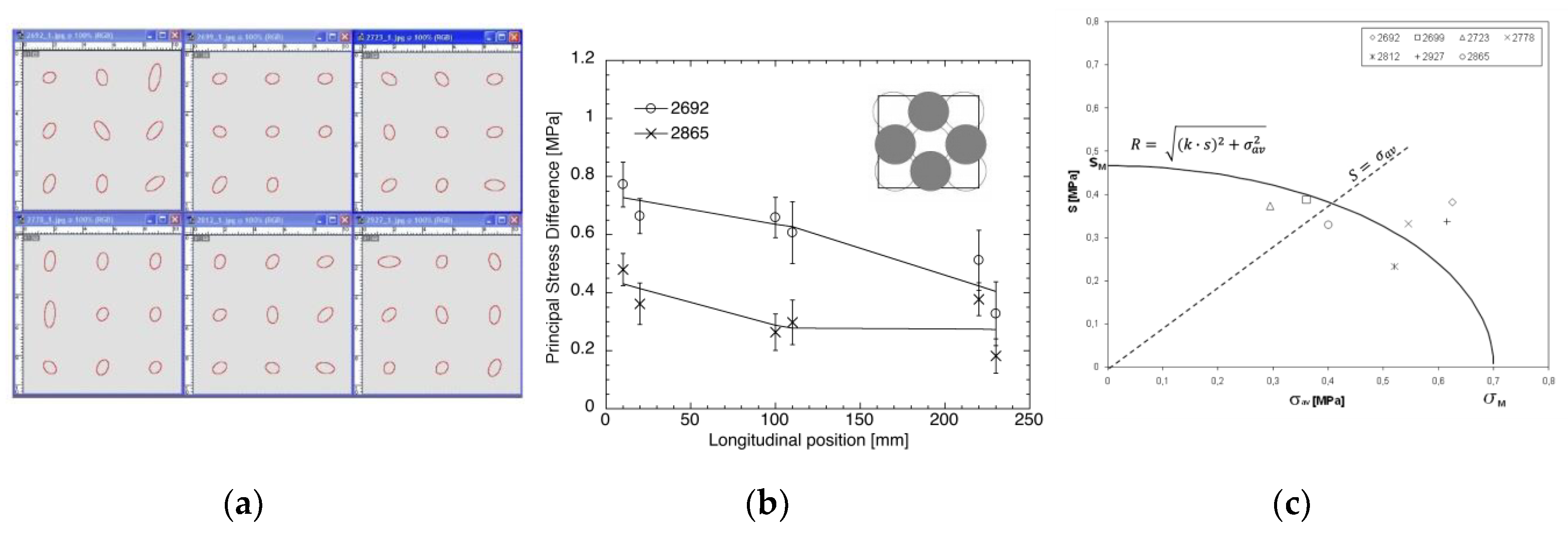
39] has been inspected by conoscopy. Observations allowed for evaluating the residual stress, due to the production process, as a signature of the whole quality of both the crystals and their manufacturing procedure. The residual stress state is an indication of a correct production process, from growth to machining and final finishing. This is linked to the general quality of the scintillators. Scintillation can be affected, and unwanted failures may arise even due to the interaction with heavy particles like hadrons. Two ingots were cut into slices and inspected in different positions. Since the observations were performed along the optic axis, the evaluation of the residual stress was carried out by the detection of the ellipticity.
Figure 4a schematically reports the ellipticities of six points over the surface of six slices. In the graph in
Figure 4b, the averaged residual stress in different positions is reported. The photoelastic method has allowed the selection of higher-quality samples and has given indications for tuning the growth parameters properly, thus enhancing the production yield. In that work [
15] a quality index has been proposed for the selection of suitable crystals (
Figure 4c). That index is defined as
R= [(kS)2+σ2av]1/2, where
σav is the average value of stress, while
S is the standard deviation. The coefficient k≥1 is related to the producer experience, which weights the dispersion of the data.
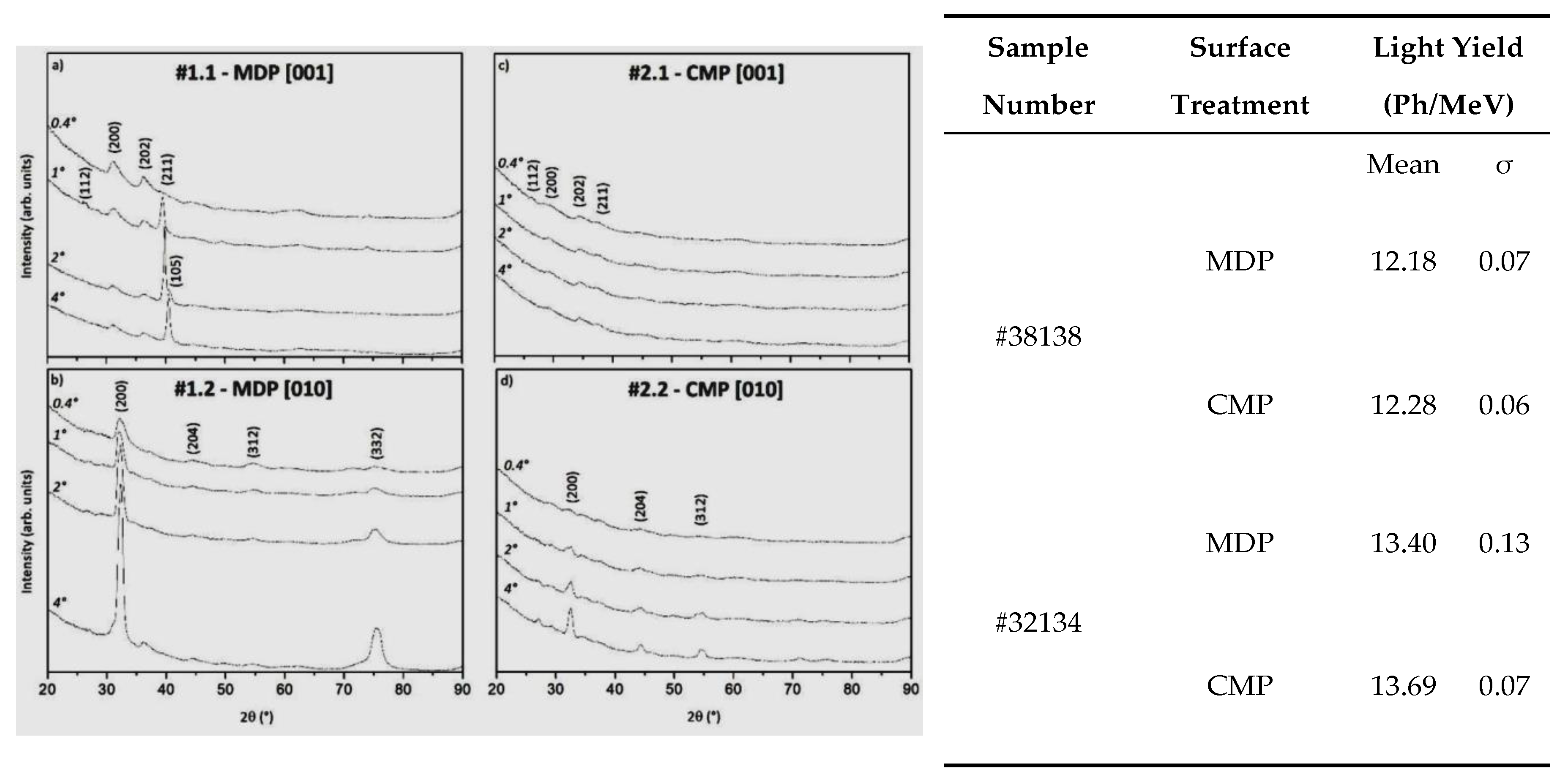
In PWOs for the CMS experiment, the influence of surface finishing has been also studied, exploiting the GID analysis [
40]. Samples were prepared and treated by different surface finishing techniques. GID analysis was used to investigate the surface structure of PWO single crystals submitted to two different finishing processes, mechanical diamond polishing (MDP) and chemical mechanical polishing. GID has clearly shown that CMP tends to amorphize the crystal surface, while the surface crystallinity is maintained when the MDP finishing process is adopted (
Figure 5). The results gave a clear indication of how to choose the optimal surface treatment for improving crystal light collection. In the same paper, the results of GID analysis and light yield test were compared, highlighting the positive contribution of the CMP treatment to the optical performance of crystals (Table 1 in
Figure 5) [
13]. In fact, CMP generates an amorphized but smoother surface that contributes to an enhanced light yield.
A fruitful combination of techniques can be found in a recent paper [
14] on modern PWOs (faster and with enhanced light yield). In that work laser conoscopy and sphenoscopy were used to inspect a defective PWO crystal as a pre-series sample for the PANDA experiment in FAIR [
9,
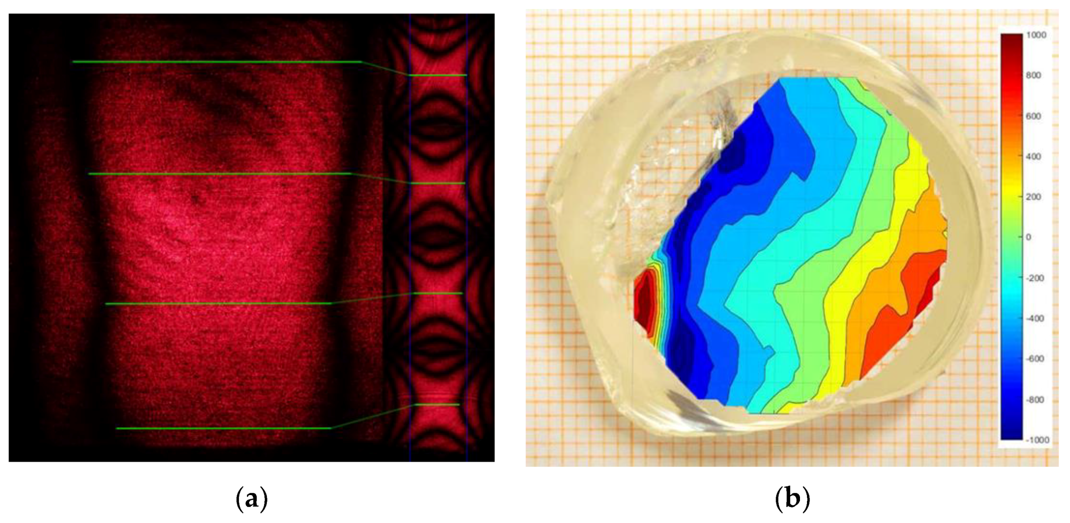
41]; the assessment of the quality was completed by XRD and EDS analysis, obtaining structural and compositional information. Since the sample was cut along the a–c crystallographic plane, the fringe patterns for each point of inspection were similar to
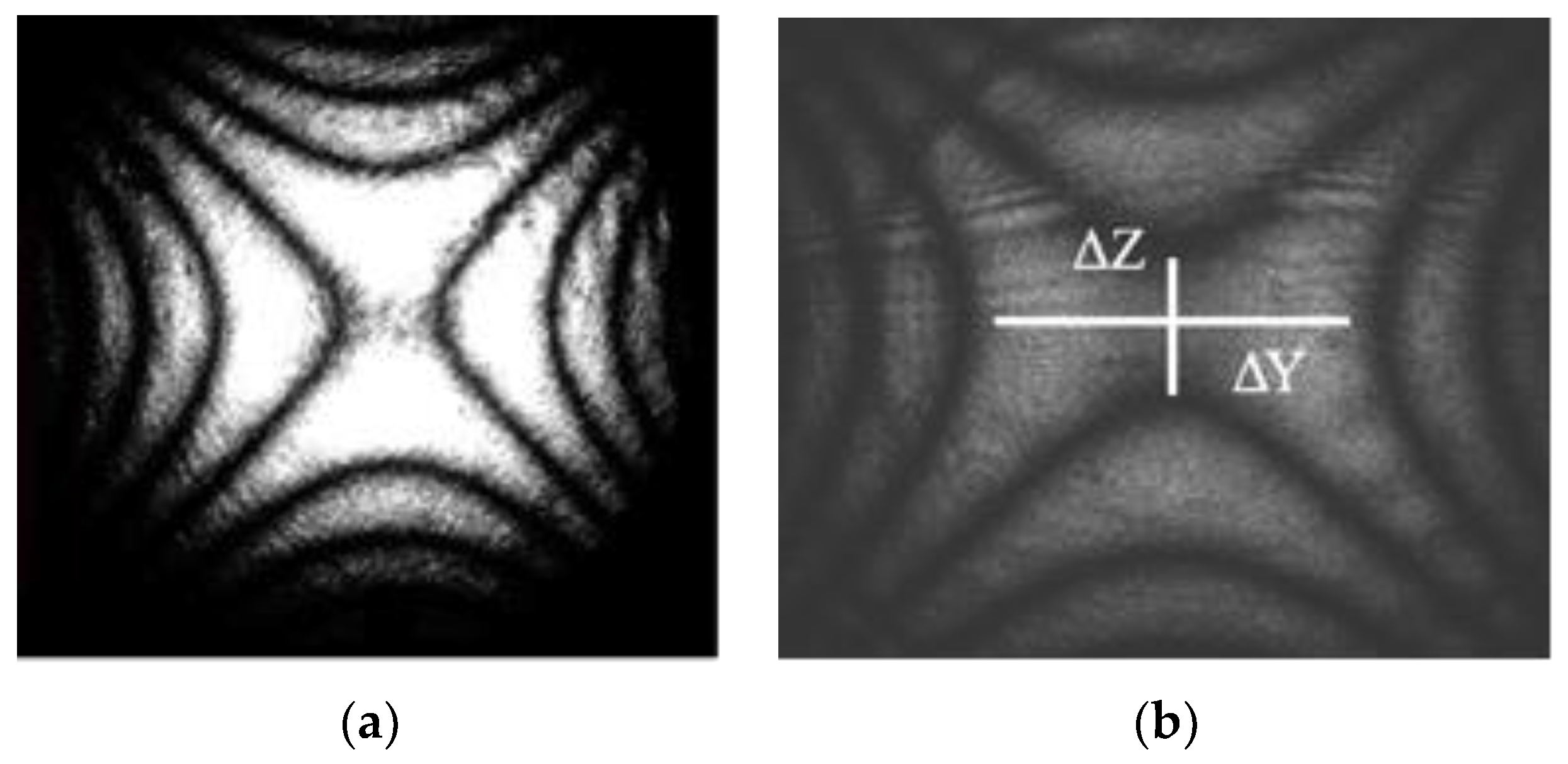
Figure 2. A map of relative stress distribution has been achieved by the conoscopic and sphenoscopic techniques (
Figure 6b). In
Figure 6a the conoscopic and sphenoscopic images are reported one beside the other.
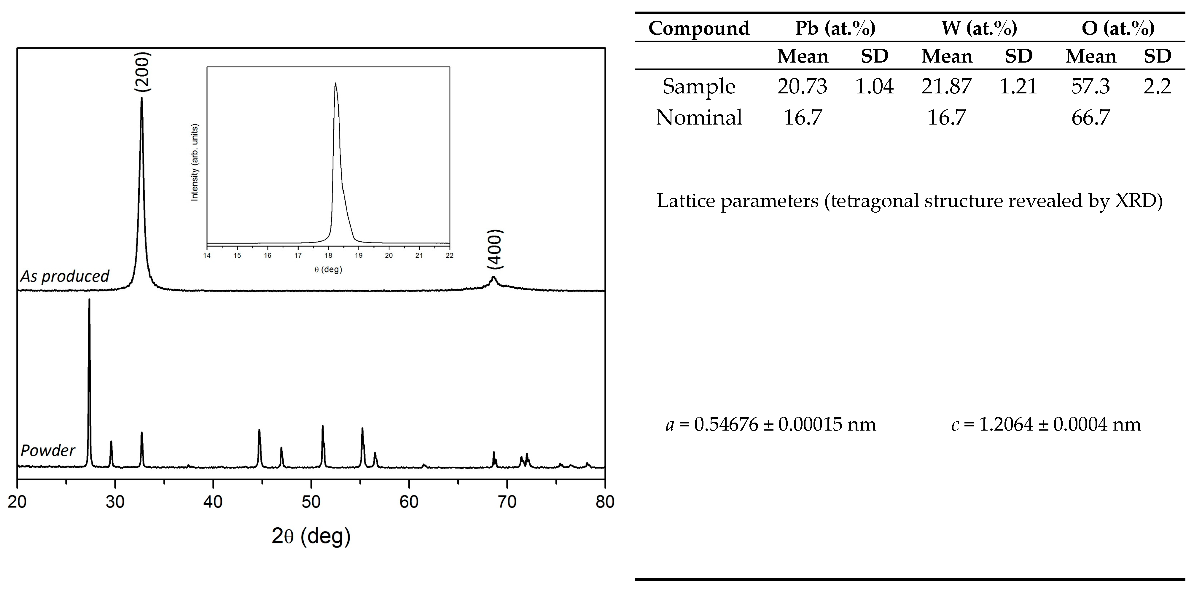
Patterns shown in
Figure 7a were obtained from the XRD analysis, providing information on crystallinity and lattice parameters that are reported in Table 2 in
Figure 7 (bottom). Table 2 in
Figure 7 also shows the results of EDS analysis, where the Pb, W, and O atomic concentrations are reported as average values (AV) and standard deviations (SD). XRD analysis and conoscopy are in agreement on the angular misalignment between crystallographic plane and sample surface. In particular, the XRD measurement in rocking curve mode (inset in
Figure 7) estimated an angular shift of the PWO (200) lattice planes of 4° with respect to the expected position. During conoscopy measurements, to obtain a symmetric fringe pattern (as in
Figure 2), the sample was tilted to the same angular value (4°) from the observation direction.
Techniques like XRD, SEM, and TEM allowed for correlating mechanical properties to the structural characteristics of cerium-doped lutetium yttrium oxyorthosilicate crystals (Lu
2(1_x) Y
2xSiO
5:Ce namely LYSO:Ce) for medical imaging devices [
42,
43,
44] in [
45]. Ultimate tensile stress (UTS) and Young’s modulus (YM) were measured in [
7,
46]. Five of them were correlated to their structural and compositional condition [
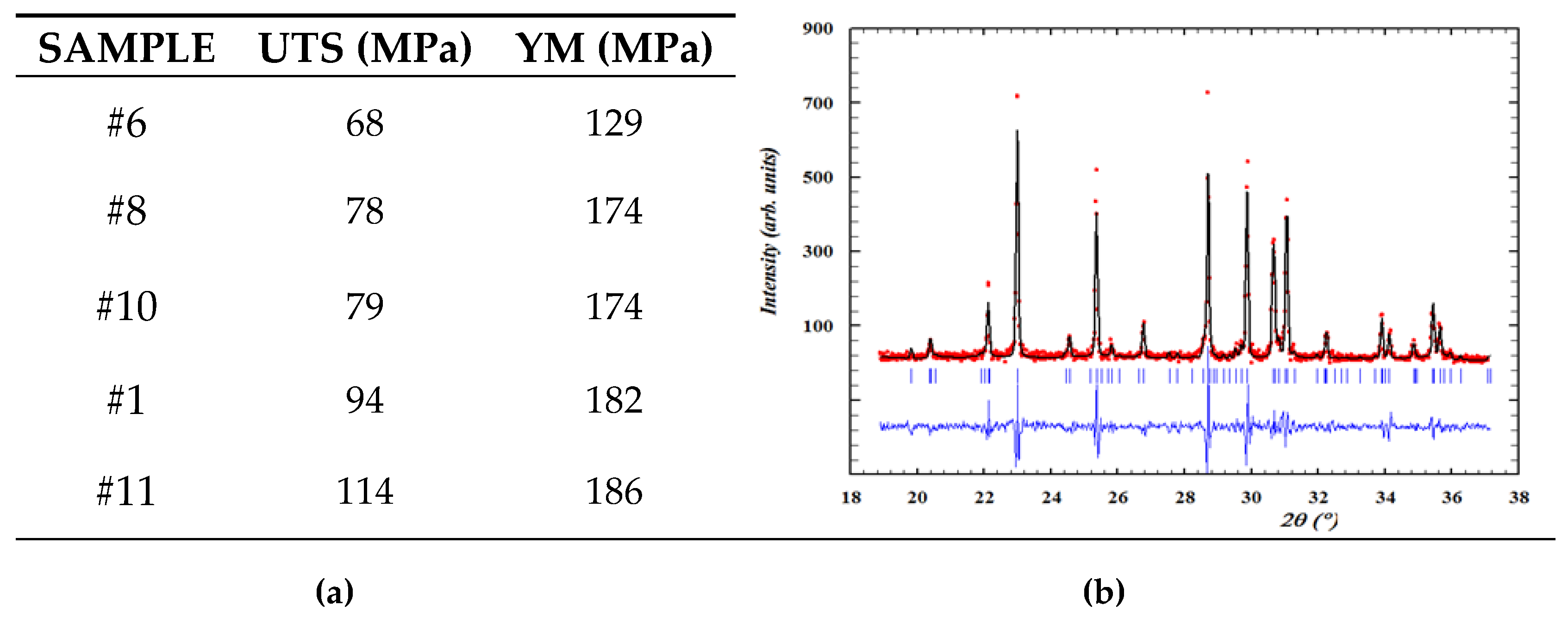
45]. Table 3, along with
Figure 8, shows the UTS and YM values of samples. XRD analysis of samples provided the patterns reported in
Figure 8. Rietveld analysis of the XRD patterns allowed for calculating the lattice parameters, which were in close agreement with the literature data.
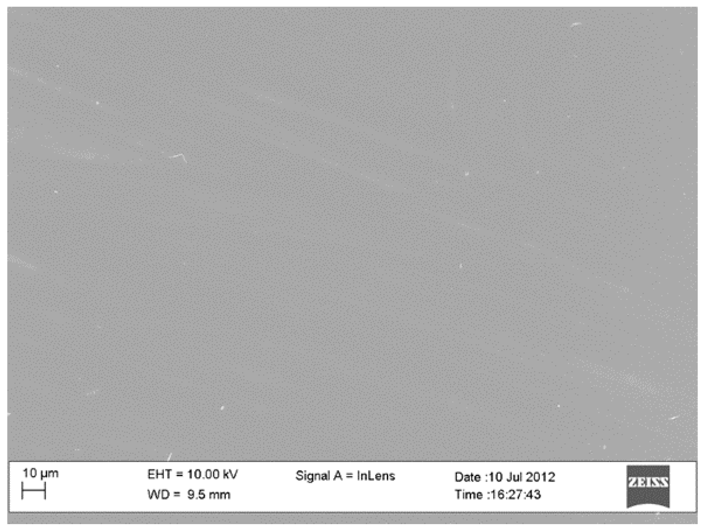
By SEM microscopy, surface finishing of samples has been observed. In
Figure 9 a typical surface presenting no evidence of macro defects is shown.
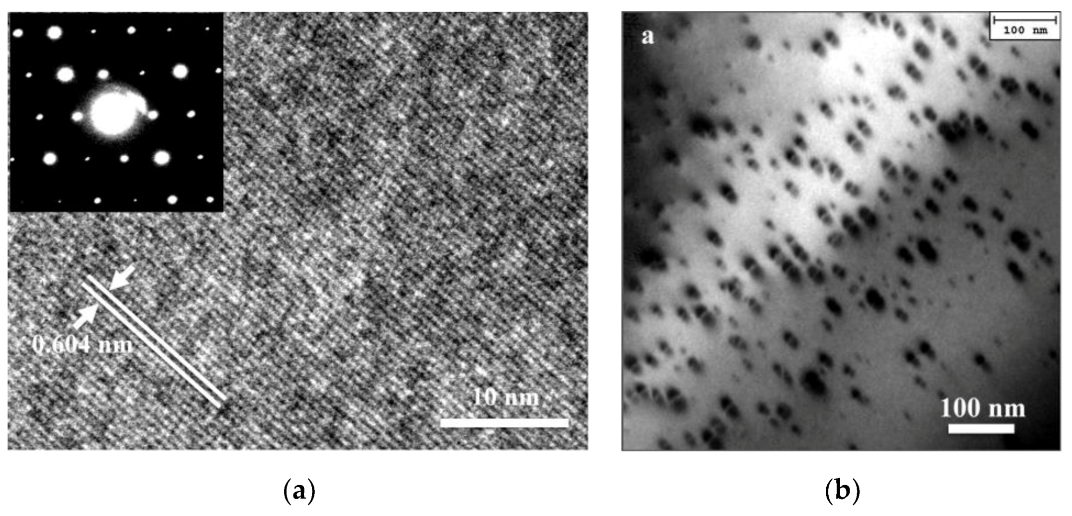
TEM measurements were performed on all five samples and the absence of lattice defects, in four out of the five samples, was confirmed by high-resolution analysis (
Figure 10a). A completely different microstructure has been revealed in sample #6, the one with the lowest UTS and YM values.
In fact, despite confirmation of the sample monoclinic structure, a non-homogenous distribution of crystallographic defects has been found.
Figure 10b shows a typical “coffee bean” contrast, indicating the presence of coherent particles showing spherically symmetrical strains with the matrix. EDX analysis has revealed an excess of Lu and Y in these defective areas, suggesting in the inhomogeneous distribution of these elements the origin of the coherent nanoparticles’ formation.
Characterization techniques are crucial for developing new materials to understand which mechanisms rule the behavior of scintillators. In fact, the influence of annealing temperature has been studied by XRD analysis to develop DSB and DSL scintillators [
47].
The patterns in
Figure 11 highlight how the crystallinity state of the orthorhombic structure varies with a temperature increase in both samples. Therefore, clear indications on the optimization of the production procedure can be achieved from a structural analysis performed by different analytical techniques.
The requirements of the application fields are pushing research toward the production of high-quality scintillators shaped like fibers. Their production processes are even more complex than bulky crystals’ [
48]. The surface to volume ratio of these scintillators is typically extremely high; therefore, the surface condition is critical as well as the crystallinity.
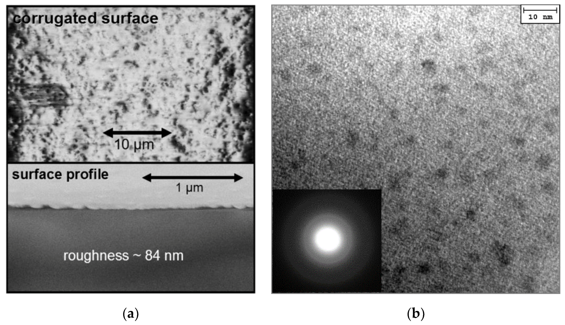
Figure 12a shows two SEM images of a LYSO fiber surface produced by the micro-pulling-down (MPD) technique [
49]. The surficial roughness can be easily evaluated and measured on large areas of the sample. Due to the dimensions and shape of a LUAG fiber (MDP produced), the sample crystallinity was evaluated by the TEM technique. In particular, TEM analysis revealed that the LUAG fiber is composed of an amorphous matrix with some crystalized nanoparticles (
Figure 12b). Due to the shape and dimension of the samples, SEM and TEM techniques are, in these cases, the best possible choice for a structural assessment.
5. Conclusions
The methodologies and measurement techniques presented in this paper provide a wide range of possibilities of exploring and investigating the structural quality of the anisotropic crystals. These techniques may be thought of as complementary to each other; from a macroscopic scale to micro and nanometric features, a complete characterization can be achieved by implementing different methodologies. Innovative laser conoscopy and sphenoscopy are particularly convenient for the quick and non-invasive inspection of crystal macroscopic conditions. Lattice macroscopic distortions due to the presence of residual stress and/or defectiveness can be easily detected. They are particularly helpful in scenarios like the inspection of the complete production of crystals at the grower level and the inspection of incoming samples for detectors assembly; in these situations non-invasiveness and speed are crucial.
More intimate inspections are allowed by the X-ray diffractometry techniques and electron microscopy. In fact, the quality of the lattice and its parameters can be evaluated with accuracy by XRD. This enables us to characterize the crystallinity and the possible lattice distortions due to inclusions, defects, and/or an incorrect growing process. GID is an extremely accurate method for assessing surfaces that are the crucial interfaces for light collection and extraction. SEM is a powerful tool at a different level; the morphology of surface and particles can be studied at micro and nanometric scale. By energy dispersion spectrometry, qualitative and quantitative evaluation of the compounds can be carried out. In case of the necessity of atomic resolution, TEM offers the possibility of detecting lattice distortion, inclusions, and possible modification of the crystal cell.
Structural analysis and quality control are fundamental in both theoretical research and the production process. Except for conditions in which a specific characteristic of the tests is needed (time, non-invasiveness, resolution, etc.), a combination of the presented methodologies is preferred, aiming at a complete characterization of the anisotropic crystals.
Author Contributions
Conceptualization, N.P., L.S., D.R., F.D. and L.M.; methodology, N.P., L.S., D.R. and L.M., G.B., P.M.; software, L.M., P.P.N.; validation, L.S., L.M. and.; formal analysis, L.M., D.N., G.B., and F.D.; investigation, L.S., L.M., D.R.; resources, L.M., P.M., G.B., D.N.; data curation, L.S., G.B., P.M., D.R. and L.M.; writing—original draft preparation, L.M.; writing—review and editing, N.P., L.S., F.D. and L.M.; visualization, G.B. and P.M.; supervision, L.M. and D.R.; project administration, L.M. and F.D.; funding acquisition, N.P., L.S. and F.D.
Funding
This research was partially funded by the European Research Council under the COST action TD-1401 “FAST-Fast Advanced Scintillation Timing” and by the research grant of the Università Politecnica delle Marche: Progetto Strategico di Ateneo 2017: “Scintillating crystals: an interdisciplinary, applications-oriented approach aimed to the scientific knowledge and process control for application concerning life-quality improvement.”
Acknowledgments
These research topics are within the scope of CERN R&D Experiment 18 “Crystal Clear Collaboration” and the PANDA Collaboration at GSI-Darmstadt.
Conflicts of Interest
The authors declare no conflict of interest. The funders had no role in the design of the study; in the collection, analyses, or interpretation of data; in the writing of the manuscript; or in the decision to publish the results.
Abbreviations
The following abbreviations are used in this manuscript:
| DICEA | Dipartimento di Ingegneria Civile, Edile e Architettura |
| DIISM | Dipartimento di Ingegneria Meccanica e Scienze Matematiche |
| SIMAU | Dipartimento di Scienze e Ingegneria della Materia, Ambiente e Urbanistica |
| ICRYS | Centro Interdipartimentale di Ricerca e Analisi Globale dei Cristalli |
| CERN | European Center for Nuclear Research, Geneva (CH) |
| PANDA | Proton Annihilation in Darmstadt, GSI, Darmstadt (D) |
| CMS | Compact Muon Solenoid |
References
- Lecoq, P. Development of new scintillators for medical applications. Nucl. Instrum. Methods Phys. Res. Sect. A Accel. Spectrom. Detect. Assoc. Equip. 2016, 809, 130–139. [Google Scholar] [CrossRef]
- Brudanin, V.B.; Gundorin, N.A.; Filossofov, D.V.; Nemtchenok, I.B.; Smolnikov, A.A.; Vasiliev, S.I.; Bregadze, V.I. Element-loaded organic scintillators for neutron and neutrino physics. In The Identification Dark Matter, Proceedings of the 3 rd International Workshop, York, UK, 18–22 September 2011; World Scientific Publishing Co. Pte. Ltd.: Singapore, 2011; No. 6; pp. 6626–6634. [Google Scholar]
- Zhu, R.Y. The next generation of crystal detectors. J. Phys. Conf. Ser. 2015, 587. [Google Scholar] [CrossRef]
- Sidletskiy, O. Trends in Search for Bright Mixed Scintillators. Phys. Status Solidi Appl. Mater. Sci. 2018, 215, 1701034. [Google Scholar] [CrossRef]
- Gundacker, S.; Auffray, E.; Pauwels, K.; Lecoq, P. Measurement of intrinsic rise times for various L(Y)SO and LuAG scintillators with a general study of prompt photons to achieve 10 ps in TOF-PET. Phys. Med. Biol. 2016, 61. [Google Scholar] [CrossRef] [PubMed]
- Lecoq, P. Pushing the Limits in Time-of-Flight PET Imaging. IEEE Trans. Radiat. Plasma Med. Sci. 2017, 1, 473–485. [Google Scholar] [CrossRef]
- Scalise, L.; Rinaldi, D.; Davì, F.; Paone, N. Measurement of ultimate tensile strength and Young modulus in LYSO scintillating crystals. Nucl. Instrum. Methods Phys. Res. Sect. A Accel. Spectrom. Detect. Assoc. Equip. 2011, 654. [Google Scholar] [CrossRef]
- Ishii, M.; Harada, K.; Kobayashi, M.; Usuki, Y.; Yazawa, T. Mechanical properties of PbWO4 scintillating crystals. Nucl. Instrum. Methods Phys. Res. Sect. A Accel. Spectrom. Detect. Assoc. Equip. 1996, 376, 203–207. [Google Scholar] [CrossRef] [Green Version]
- Boca, G. The PANDA experiment: Physics goals and experimental setup. EPJ Web Conf. 2014, 72, 2. [Google Scholar] [CrossRef]
- Donghia, R. The Mu2e experiment at Fermilab: Design and status. NUOVO Cim. 2017, 40, 1–7. [Google Scholar]
- Kimble, T.; Chou, M.; Chai, B.H.T. Scintillation properties of LYSO crystals. In Proceedings of the 2002 IEEE Nuclear Science Symposium Conference Record, Norfolk, VA, USA, 10–16 November 2002; Volume 3, pp. 1434–1437. [Google Scholar]
- Ding, D.Z.; Yang, J.H.; Ren, G.H.; Nikl, M.; Wang, S.; Wu, Y.T.; Mao, Z.Y. Effects of anisotropy on structural and optical characteristics of LYSO: CE crystal. Phys. Status Solidi Basic Res. 2014, 251, 1202–1211. [Google Scholar] [CrossRef]
- Rinaldi, D.; Montalto, L.; Lebeau, M.; Mengucci, P. Influence of a Surface Finishing Method on Light Collection Behaviour of PWO Scintillator Crystals. Photonics 2018, 5, 47. [Google Scholar] [CrossRef]
- Montalto, L.; Natali, P.P.; Daví, F.; Mengucci, P.; Paone, N.; Rinaldi, D. Characterization of a defective PbWO4 crystal cut along the a-c crystallographic plane: Structural assessment and a novel photoelastic stress analysis. J. Instrum. 2017, 12. [Google Scholar] [CrossRef]
- Rinaldi, D.; Ciriaco, A.; Lebeau, M.; Paone, N. Quality control on pre-serial Bridgman production of PbWO4 scintillating crystals by means of photoelasticity. Nucl. Instrum. Methods Phys. Res. Sect. A Accel. Spectrom. Detect. Assoc. Equip. 2010, 615, 254–258. [Google Scholar] [CrossRef]
- Dally, J.W.; Riley, W.F. Experimental Stress Analysis; Kogushka McGraw Hill: Toledo, OH, USA, 1966. [Google Scholar]
- Coker, E.G.; Filon, L.N.G. A Treatise on Photo-Elasticity; Cambridge University Press: Cambridge, UK, 1931. [Google Scholar]
- Ewing, J.A. Photo—Elasticity; Nature Publishing Group: London, UK, 1932. [Google Scholar]
- Born, M.; Wolf, E. Principles of Optics: Electromagnetic Theory of Propagation, Interference and Diffraction of Light; Cambridge university press: Cambridge, UK, 1955. [Google Scholar]
- Wahlstrom, E.E. Optical Crystallography; Wiley: Hoboken, New Jersey, USA, 1969. [Google Scholar]
- Rinaldi, D.; Ietroni, P.P.; Davì, F. Isochromate fringes simulation by Cassini-like curves for photoelastic analysis of birefringent crystals. Nucl. Instrum. Methods Phys. Res. Sect. A Accel. Spectrom. Detect. Assoc. Equip. 2009, 603, 294–300. [Google Scholar] [CrossRef]
- Daví, F. On the Bertin surfaces of photoelastic crystals. J. Opt. Soc. Am.A 2015, 32, 2323. [Google Scholar] [CrossRef] [PubMed]
- Daví, F.; Rinaldi, D. Mechanical and Optical Properties of Anisotropic Single-Crystal Prisms. J. Elast. 2015, 120, 197–224. [Google Scholar] [CrossRef]
- Rinaldi, D.; Daví, F.; Montalto, L. On the photoelastic constants and the Brewster law for stressed tetragonal crystals. Math. Methods Appl. Sci. 2018, 41, 3103–3116. [Google Scholar] [CrossRef]
- Ciriaco, A.; Davi, F.; Lebeau, M.; Majni, G. PWO photo-elastic parameter calibration by laser-based polariscope. Nucl. Instrum. Methods Phys. Res. Sect. A Accel. Spectrom. Detect. Assoc. Equip. 2007, 570, 55–60. [Google Scholar] [CrossRef]
- Natali, P.P.; montalto, L.; Davi, F.; Menqucci, P.; Paone, N.; Rinaldi, D. Theoretical and experimental evaluation of piezo-optic parameters and photoelastic constant in tetragonal PWO. Appl. Opt. 2018, 57, 730–737. [Google Scholar] [CrossRef]
- Mytsyk, B.G.; Andrushchak, A.S.; Demyanyshyn, N.M.; Kost, Y.P.; Kityk, A.V.; Mandracci, P.; Schranz, W. Piezo-optic coefficients of MgO-doped LiNbO_3 crystals. Appl. Opt. 2009, 48, 1904–1911. [Google Scholar] [CrossRef]
- Solskii, I.M.; Mytsyk, B.G.; Kost, Y.P.; Andrushchak, A.S.; Demyanyshyn, N.M. Piezo-optic coefficients of CaWO4 crystals. Crystallogr. Rep. 2015, 60, 130–137. [Google Scholar]
- Mytsyk, B.G.; Dem yanyshyn, N.M. Piezo-optic surfaces of lithium niobate crystals. Crystallogr. Rep. 2006, 51, 653–660. [Google Scholar] [CrossRef]
- Natali, P.P.; Montalto, L.; Rinaldi, D.; Davi, F.; Paone, N.; Scalise, L. Noninvasive Inspection of Anisotropic Crystals: Innovative Photoelasticity-Based Methods. IEEE Trans. Nucl. Sci. 2018, 65, 2203–2207. [Google Scholar] [CrossRef]
- Montalto, L.; Paone, N.; Scalise, L.; Rinaldi, D. A photoelastic measurement system for residual stress analysis in scintillating crystals by conoscopic imaging. Rev. Sci. Instrum. 2015, 86, 86. [Google Scholar] [CrossRef] [PubMed]
- Montalto, L.; Paone, N.; Rinaldi, D.; Scalise, L. Inspection of birefringent media by photoelasticity: From diffuse light polariscope to laser conoscopic technique. Opt. Eng. 2015, 54. [Google Scholar] [CrossRef]
- Montalto, L.; Rinaldi, D.; Scalise, L.; Paone, N.; Davì, F. Photoelastic sphenoscopic analysis of crystals. Rev. Sci. Instrum. 2016, 87. [Google Scholar] [CrossRef] [PubMed]
- Klug, H.P.; Alexander, L.E. X-Ray Diffraction Procedures—For Polycrystalline and Amorphous Materials; Wiley: New York, NY, USA, 1974. [Google Scholar]
- Nielsen, J.A.; McMorrow, D. Elements of Modern X-Ray Physics, 2011th ed.; J. Wiley & Sons Ltd.: Hoboken, NJ, USA, 2011. [Google Scholar]
- Cullity, B.D.; Stock, S.R. Elements of X-Ray Diffraction, 2014th ed.; Pearson Education Ltd.: Upper Saddle River, NJ, USA, 2014. [Google Scholar]
- Goldstein, J.; Newbury, D.E.; Joy, D.C.; Lyman, C.E.; Echlin, P.; Lifshin, E.; Sawyer, L.; Michael, J. R Scanning Electron Microscopy and X-Ray Microanalysis; Springer: New York, NY, USA, 1992. [Google Scholar]
- Hirsch, P.B. Electron Microscopy of Thin Crystals; Krieger Publishing Company: Malabar, FL, USA, 1977. [Google Scholar]
- Rudolph, P.; Kiessling, F. The horizontal bridgman method. Cryst. Res. Technol. 1988, 23, 1207–1224. [Google Scholar] [CrossRef]
- Mengucci, P.; Cristoforo, A.D.; Lebeau, M.; Majni, G.; Paone, N.; Pietroni, N.; Rinaldi, D. Surface quality inspection of PbWO4 crystals by grazing incidence X-ray diffraction. Nucl. Instrum. Methods Phys. Res. Sect. A Accel. Spectrom. Detect. Assoc. Equip. 2005, 537. [Google Scholar] [CrossRef]
- Barucca, G.; Davı, F.; Lancioni, G.; Mengucci, P.; Montalto, L.; Natali, P.P.; Paone, N.; Rinaldi, D.; Scalise, L.; Erni, W. Precision resonance energy scans with the PANDA experiment at FAIR: Sensitivity study for width and line shape measurements of the X(3872). Eur. Phys. J. A 2019, 55. [Google Scholar] [CrossRef]
- David, S.; Georgiou, M.; Fysikopoulos, E.; Loudos, G. Evaluation of a SiPM array coupled to a Gd3Al2Ga3O12:Ce (GAGG:Ce) discrete scintillator. Phys. Med. 2015, 31, 763–766. [Google Scholar] [CrossRef]
- Pizzichemi, M. Positron Emission Tomography: State of the art and future developments. J. Instrum. 2016, 11. [Google Scholar] [CrossRef]
- Auffrayc, E.; Bel Hadjc, F.B.M.; Cortinovisa, D.; Doroudc, K.; Garuttib, E.; Lecoqc, P.; Liud, Z.; Martinezd, R.; Paganonid, M.; Pizzichemid, M.; et al. Characterization studies of silicon photomultipliers and crystals matrices for a novel time of flight PET detector. J. Instrum. 2015, 10, P06009. [Google Scholar] [CrossRef]
- Menguccia, P.; Andréb, G.; Auffrayc, E.; Baruccaa, G.; Cecchi, C.; Chipauxe, R.; Cousson, A.; Davì, F.; Di Vara, N.; Rinaldia1, D.; et al. Structural, Mechanical and light yield characterisation of heat treated LYSO:Ce single crystals for medical imaging applications. Nucl. Instrum. Methods Phys. Res. Sect. A Accel. Spectrom. Detect. Assoc. Equip. 2015, 785, 110–116. [Google Scholar] [CrossRef]
- Davi, F.; Rinaldi, D. Elastic moduli and optical properties of LYSO crystals: Theory and experiments. IEEE Trans. Nucl. Sci. 2012, 59. [Google Scholar] [CrossRef]
- Trusova, E.; Vaitkevičius, A.; Tratsiak, Y.; Korjik, M.; Mengucci, P.; Rinaldi, D.; Montalto, L.; Marciulionyte, V.; Tamulaitis, G. Barium and lithium silicate glass ceramics doped with rare earth ions for white LEDs. Opt. Mater. Amst. 2018, 84, 459–465. [Google Scholar] [CrossRef]
- Leutz, H. Scintillating fibres. Nucl. Instrum. Methods Phys. Res. Sect. A Accel. Spectrom. Detect. Assoc. Equip. 1995, 364, 422–448. [Google Scholar] [CrossRef] [Green Version]
- Diehl, S.; Novotny, R.; Aubry, N.; Faraj, S.; Ferro, G. Development and Characterization of Inorganic Scintillating Fibers Made of LuAG:Ce and LYSO:Ce. IEEE Trans. Nucl. Sci. 2014, 61. [Google Scholar] [CrossRef]
© 2019 by the authors. Licensee MDPI, Basel, Switzerland. This article is an open access article distributed under the terms and conditions of the Creative Commons Attribution (CC BY) license (http://creativecommons.org/licenses/by/4.0/).


 ,
, 


