Pulse-Propagation Modeling and Experiment for Femtosecond-Laser Writing of Waveguide in Nd:YAG
by
Tao Feng
1,2, 
Pankaj K. Sahoo
1,
Francisco R. Arteaga-Sierra
2,
Christophe Dorrer
2 and
Jie Qiao
1,2,* 1
Chester F. Carlson Center for Imaging Science, Rochester Institute of Technology, Rochester, NY 14623, USA
2
Aktiwave LLC, 150 Lucius Gordon Dr., Rochester, NY 14586, USA
*
Author to whom correspondence should be addressed.
Crystals 2019, 9(8), 434; https://0-doi-org.brum.beds.ac.uk/10.3390/cryst9080434
Submission received: 19 July 2019
/
Revised: 9 August 2019
/
Accepted: 16 August 2019
/
Published: 20 August 2019
(This article belongs to the Special Issue Laser Crystals)
Abstract
:In this work, unidirectional pulse propagation equation (UPPE) modeling is performed to study the nonlinear laser-mater interaction in silicon and Nd:Y3Al5O12 (Nd:YAG) crystals. The simulation results are validated with reported experimental results for silicon and applied to Nd:YAG crystals with experimental validation. Stress-induced waveguides are written in Nd:YAG crystals using 515 nm, 300 fs pulses at a 1 kHz repetition rate. Waveguides having a mean propagation loss of 0.21 ± 0.06 dB/cm are obtained, which is lower than the previous reported values for Type-II waveguides written in Nd:YAG crystals. The modeling and experimental results consistently show that the modification (waveguide track) depth increases with input energy. A detailed analysis is presented to control the modal properties of the waveguide in the context of UPPE simulation.
1. Introduction
Femtosecond (fs) waveguide writing is a powerful technique for the fabrication of three-dimensional photonic waveguide components in dielectric amorphous [1] and crystalline materials [2,3,4,5,6,7], semiconductors such as silicon [8] and diamond [9,10,11], and polymers like polydimethylsiloxane [12]. Among dielectric materials, YAG (Y3Al5O12) is highly suitable for writing waveguides and realizing waveguide lasers due to its excellent optical and thermomechanical properties, such as long fluorescence lifetime, high emission cross-section, and good thermal conductivity [5]. Femtosecond-laser-written waveguides are broadly classified into directly written waveguides (Type I), stress-induced waveguides (Type II), depressed cladding waveguides (Type III) and ablated ridge waveguides (Type IV) [13]. Type II waveguides are more advantageous than other types for waveguide lasers in YAG [13]. For example, they are superior to the Type III waveguides in terms of ease in fabrication and single mode profile. In Type II configuration, a fs-laser induces a negative refractive index change in the irradiated track (focal) region due to both lattice damage and induced stress [14] and a relatively high index in the nearby background through stress-induced effects. There are several reports of Type II waveguide writing in Nd:YAG crystals based on stress-induced refractive index change [3,5,13,14,15,16,17]. However, there is currently no detailed explanation of the nonlinear optical mechanisms and their impact, such as fluence evolution and plasma formation induced by multi-photon ionization (MPI) on waveguide writing. In this work, we study for the first time the underlying physics behind nonlinear optical dynamics in ultrafast laser beam propagation during the femtosecond laser processing of Nd:YAG. Unidirectional pulse propagation equation (UPPE) [18] simulation is carried out to analyze the nonlinear pulse propagation inside a Nd:YAG crystal, which provides a better understanding of how pulse energy and focusing conditions affect material modification (waveguide track) and guiding properties. Based on this UPPE modeling, a comprehensive analysis of an optimization method has been presented to control the modal properties, such as shape and propagation loss of the waveguide. The effects have been analyzed and optimized to achieve minimum propagation loss and better mode confinement.
2. Unidirectional Pulse Propagation Equation Modeling to Predict Nonlinear Dynamics in Femtosecond Laser Processing of Crystal Materials
UPPE-based numerical modeling is used to predict the spot size and peak fluence evolution of a single pulse in both longitudinal and transverse directions, using different laser parameters and focusing conditions. UPPE simulation investigates the nonlinear optical dynamics inside the Nd:YAG substrate, considering self-focusing by the Kerr effect and defocusing by plasma generation through Equation (1) [18].
where is the electric field, is the longitudinal propagation direction, is the optical frequency, are transverse wavenumbers, , and and are the nonlinear polarization and current density, respectively. Equation (1) is solved together with the kinetic equation for plasma concentration (), as given by Equation (2):
where is the initial valence electron density, is the electron collision time, is the MPI cross-section and is the MPI order. Pulse propagation in silicon is first analyzed and compared with previous reported results to validate the modeling accuracy [8]. The parameters of silicon considered in our modeling are given in Table 1 [8].
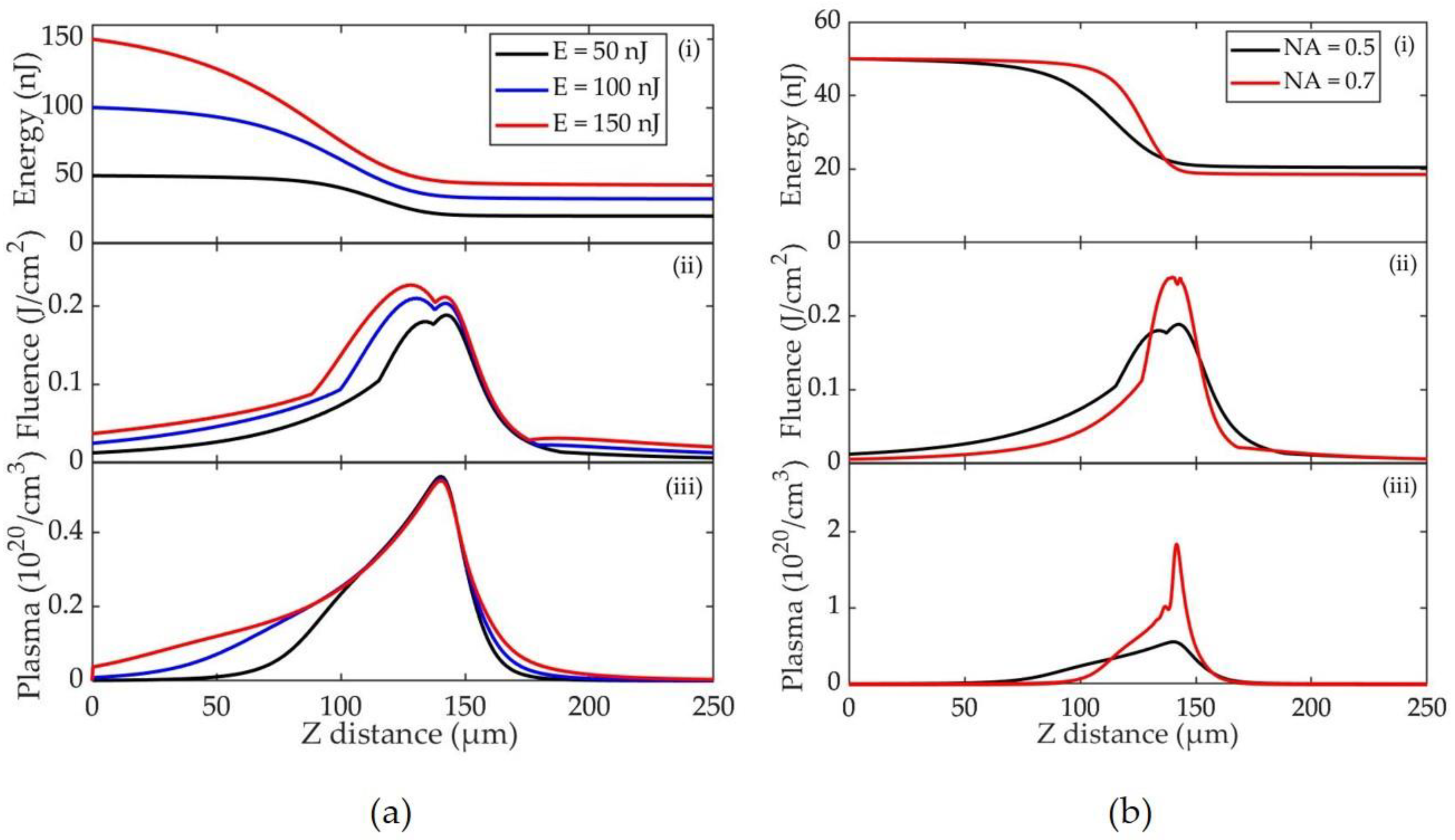
Figure 1a shows the evolution of energy, fluence, and plasma density along the propagation direction () of the laser pulse for different input energy while the laser beam is focused 150 µm below the top surface of the substrate. The numerical aperture of the focusing microscope is 0.5.
Figure 1ai shows that owing to the multi-photon absorption in the material, pulse energies are nonlinearly depleted from their initial values before reaching their respective focal planes (the minimum beam waist for each energy). When the pulse energy increases from 50 nJ to 100 nJ, then to 150 nJ, the fraction of energy arriving at the focal plane decreases from 43% to 35%, and then to 30%, respectively. Figure 1aii shows that the peak fluence increases from 0.19 J/cm2 to 0.21 J/cm2, and then to 0.23 J/cm2, when input pulse energy increases from 50 nJ to 100 nJ, and then to 150 nJ, respectively. Meanwhile, the fluence peak is shifted toward the top surface (= 0) of the substrate due to self-focusing induced by the Kerr effect. Figure 1aiii shows that while the laser pulse propagates into the material, plasma density initially increases with input energy (50 nJ to 150 nJ) and then saturates near the focal plane. This can be explained by the nonlinear dependence (Equation (2)) of plasma density on intensity. The plasma saturation near the focal region is due to the inverse Bremsstrahlung absorption and plasma defocusing dominating over the self-focusing. The details of the dependence of plasma density on intensity can be found in [8,19,20,21]. Figure 1b further compares energy, fluence, and plasma density evolution for two different focusing conditions (numerical aperture (NA) = 0.5 and 0.7) at an input energy of 50 nJ. When the NA is increased from 0.5 to 0.7, the energy depletion becomes more abrupt (steeper slope) around the focal location and 6.6% more energy is absorbed, the peak fluence increases from 0.19 J/cm2 to 0.25 J/cm2, and the plasma density increases from 0.55 × 1020 cm−3 to 1.84 × 1020 cm−3. Thus, a broadened fluence profile (broader focus) along the propagation direction can be achieved with higher pulse energy, while a narrowed fluence profile (tighter focus) can be achieved by a larger NA.
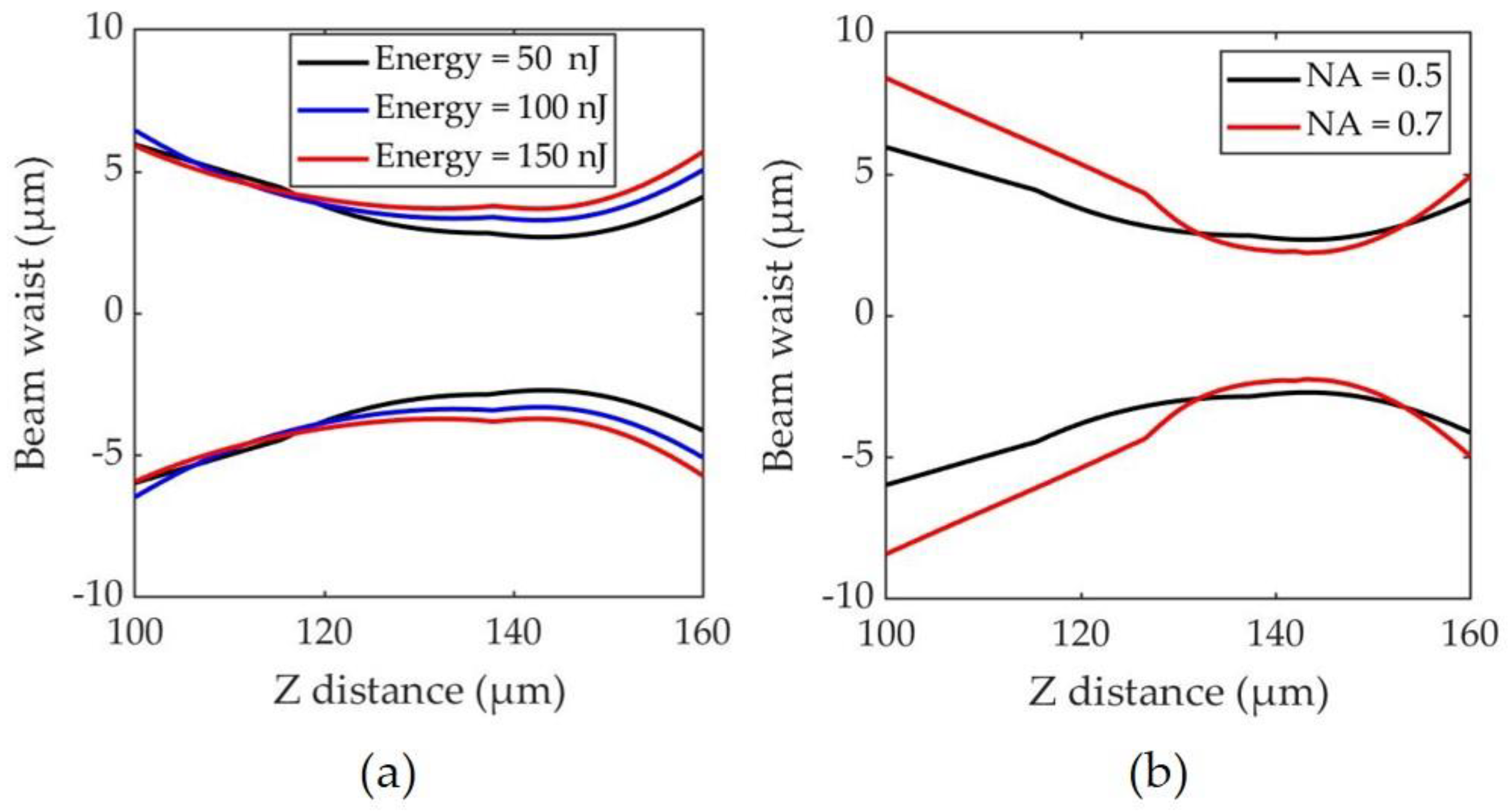
An analysis of beam waist evolution is provided to gain more insights on this effect. Figure 2 shows the beam waist (inside silicon) along the propagation direction under different energy and focusing conditions.
As shown in Figure 2a, when input energy is increased from 50 nJ to 150 nJ for NA = 0.5, the focal spot is increased from 2.70 μm to 3.70 μm due to the broadened plasma profile described in Figure 1aiii. From Figure 2b, when the NA is increased from 0.5 to 0.7 at an input energy of 50 nJ, the simulated focal spot radius slightly decreases from 2.70 μm to 2.23 μm (~17%). For the same NA variation (0.5 to 0.7), however, the calculated diffraction-limited focal spot size reduces by 34% (from 2.12 μm to 1.40 μm). This difference is owing to the increased plasma defocusing effect inside the material. Similar results were obtained for input energy values of 100 nJ and 150 nJ.
The simulation results presented above are consistent with previous experimental observation: when the pulse energy is increased, the peak fluence increases and shifts towards the top surface, and the focal volume broadens along the pulse propagation direction (see Figure 1b in [8]).
The results demonstrate that (1) it may not be an effective approach to simply increase laser-pulse energy for a given focusing condition (NA) due to the induced defocusing from the increased plasma density; (2) the sample can be more easily modified when using an objective with higher NA at certain input energy. The effectiveness of increasing NA is affected by the competition between plasma-induced defocusing and Kerr-effect-induced self-focusing; and (3) UPPE modeling can be used as an effective tool to balance these nonlinear effects and produce controlled material modification.
The UPPE model was extended to simulate femtosecond laser interaction inside Nd:YAG crystals. The Nd:YAG material parameters and other simulation parameters are provided in Table 2 [22]. A laser wavelength of 2 μm is used for the simulation due to the limited literature-reported value for the Nd:YAG MPI cross-section. However, the obtained results and observations at this wavelength can be qualitatively analyzed to provide insight into our experiment at 515 nm.
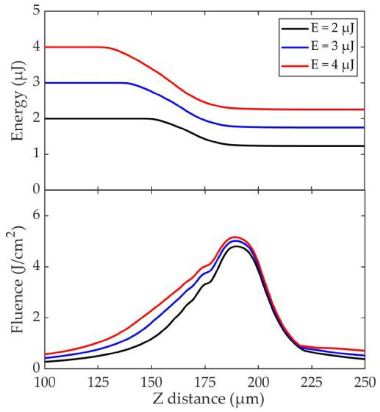
The evolutions of deposited energy and peak fluence inside Nd:YAG crystal for 0.5 NA microscope objective at three different input-energy values, 2 μJ, 3 μJ, and 4 μJ, are shown in Figure 3. The width of the fluence profile along the beam propagation direction ( direction) is larger for a higher input energy. This implies that deeper modification depth is expected to be achieved with higher pulse energy. However, when the input energy increases from 2 μJ to 4 μJ, the peak fluence only increases by 7.5%. This indicates that fluence at the focus is not very sensitive to the increase in input energy due to the nonlinear absorption of the laser pulse energy prior to arriving at the focal location. The experimental validation of these observations is discussed in Section 3.
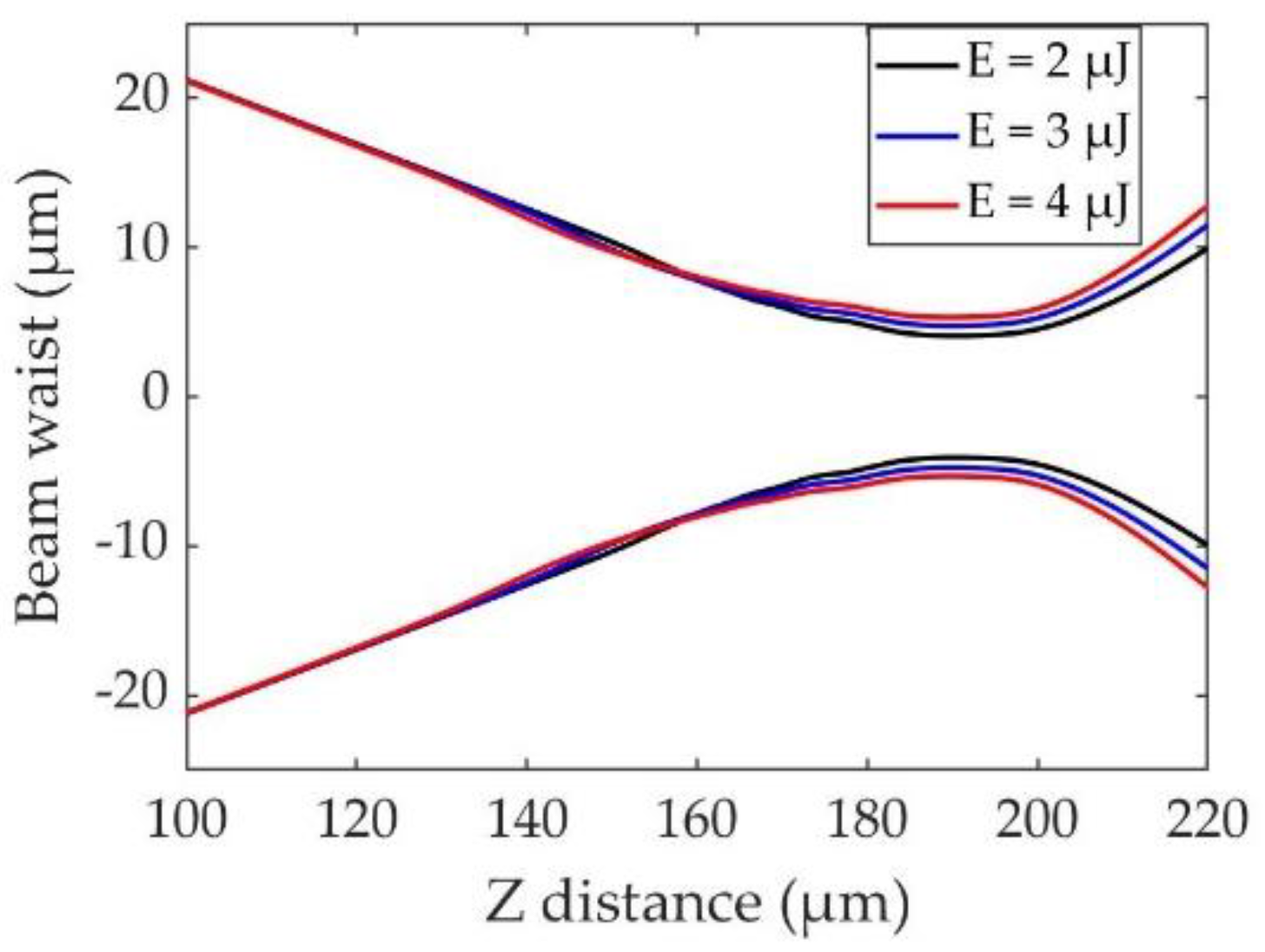
Figure 4 shows the evolution of the beam waist along the propagation. The beam waist is broadened when increasing the input pulse energy. Since the generated plasma density at higher energy defocuses the beam, the radius of the focal spot increases from 4.08 μm to 5.31 μm when the input energy is increased from 2 μJ to 4 μJ.
3. Experimental Demonstration and Modeling Validation
3.1. Waveguide Fabrication
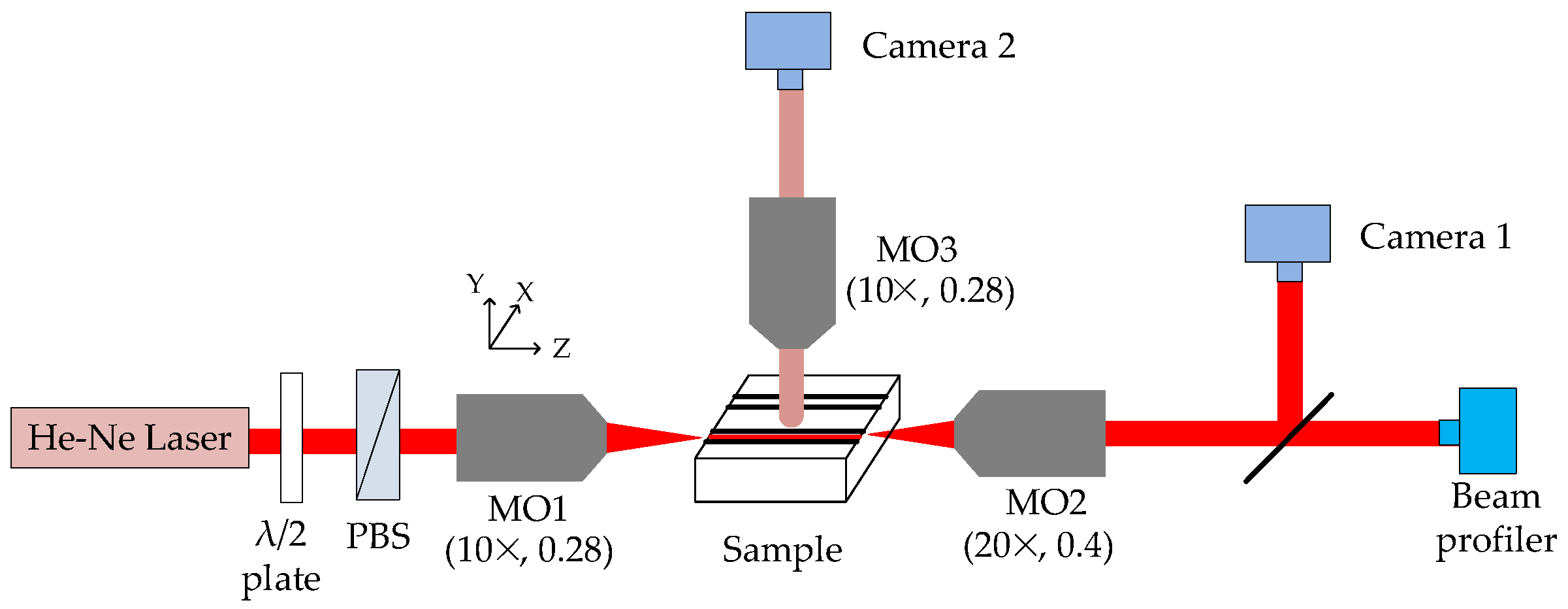
A 300 fs, 515 nm (2nd harmonic) ytterbium fiber laser (Satsuma HP3, Amplitude Systèmes, Cité de la Photonique, Pessac, France) with a repetition rate of 1 kHz is used for the fabrication of waveguides in Nd:YAG crystals (7.5 mm × 5 mm × 10 mm), cut along the crystal axes. Figure 5 shows the schematic of the experimental setup for laser waveguide writing.
The laser beam is focused into the sample, 200 μm below the surface, by a 20× microscope objective (MO, Nikon, Minato, Tokyo, Japan) with an NA of 0.5. Type II waveguides were written with various configurations. During the writing process, the sample was moved at a given velocity along the X direction by a motorized translation stage. Different pairs of tracks with separation varying from 20 µm to 30 µm were inscribed with pulse energies ranging from 2 µJ to 4 µJ.
3.2. Waveguide Characterization
A free-space coupling method as shown schematically in Figure 6 is used to characterize the guided modes in the waveguide. A He-Ne Laser beam (632.8 nm wavelength) is focused into the channel waveguides by a microscope objective 1 (MO1, Mitutoyo, Kawasaki, Japan) lens (10×, 0.28 NA). The effective NA of the objective is measured to be 0.029, due to the small input beam diameter compared to the objective aperture. The polarization of the laser beam is controlled by a polarizing beam splitter (PBS) and a plate.
The second microscope objective (MO2, Olympus, Shinjuku, Tokyo, Japan) lens (20×, 0.4 NA) images the guided mode onto a beam profiler (DataRay Inc., Redding, California, United States) for near-field beam-profile analysis. Camera 1 (Imaging Source, Charlotte, NC, United States) measures the cross-section of the fabricated waveguide. Camera 2 (Imaging Source, Charlotte, NC, United States) acquires the fluorescence excited by the laser and scattered light from the fabricated tracks. The sample is mounted on a mechanical stage with linear translation in the X and Y directions (perpendicular to the beam direction) and rotation around these two axes. The focal positions of the objectives are adjustable with their respective translation stages.
3.3. Comparison of Experimental and Modeling Results
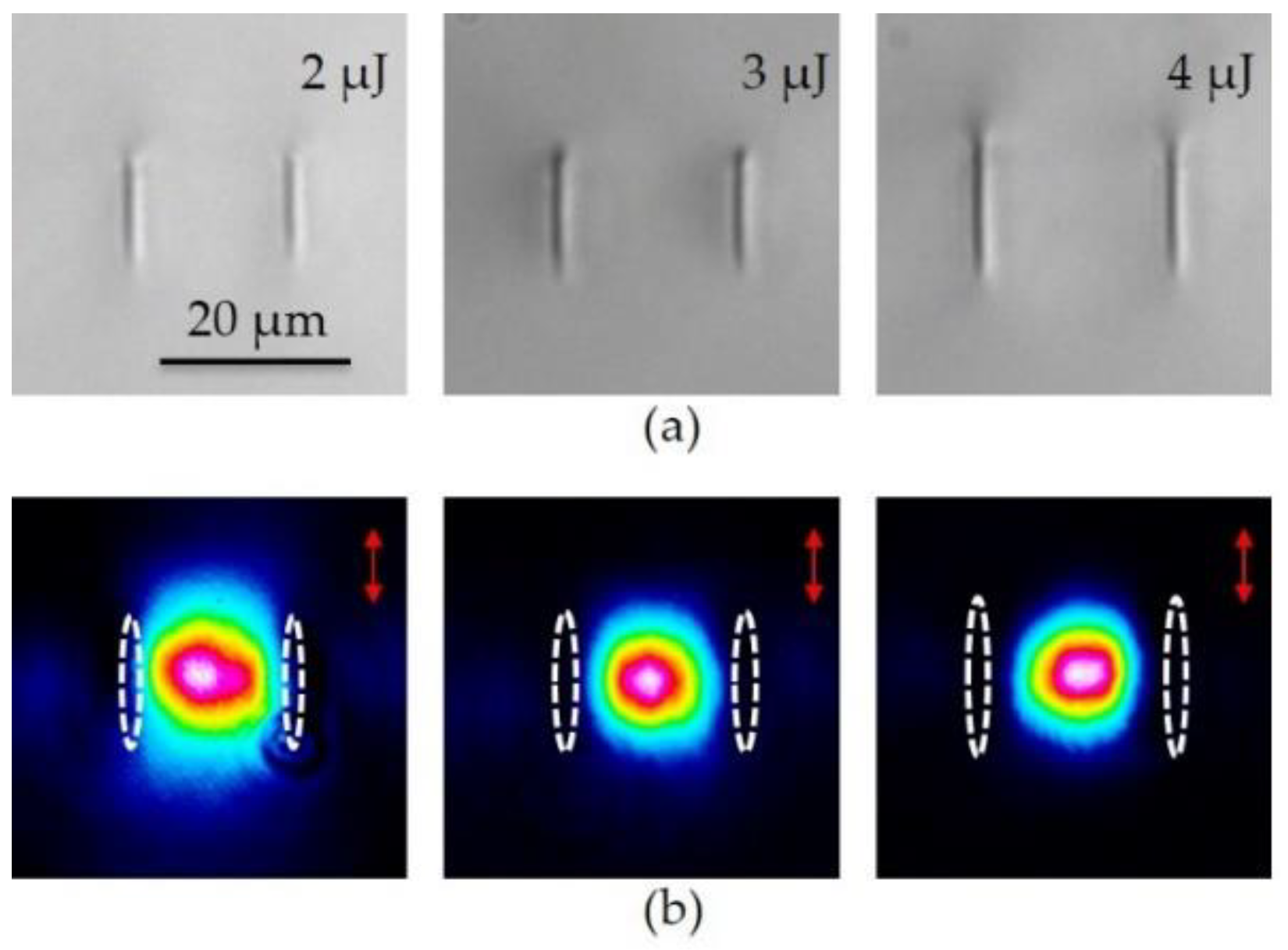
To experimentally validate the UPPE results, the effect of pulse energy on the depth of the laser induced tracks, as well as on the guided modes, is analyzed. Figure 7 shows the cross-section of the waveguide tracks and the near-field fluence maps of the guided mode when increasing the input energy from 2 μJ to 4 μJ while maintaining the scanning speed at 100 μm/s and the track separation at 20 μm. It should be noted that the polarization of the beam is kept perpendicular to the top surface of the substrate (along the Y axis, as shown in Figure 6). Only this polarization produces guided propagation between the two tracks, as has also been previously reported [5].
Figure 7a shows that the track depth increases from 12 μm to 18 μm when the pulse energy is increased from 2 μJ to 4 μJ. There is no significant change in the widths of the tracks. This experimental result is consistent with the UPPE simulation result shown in Figure 3, where the fluence profile is broadened along the longitudinal axis for higher input pulse energy, whereas the peak fluences are similar.
Figure 7b shows the near-field intensity maps of the corresponding guided modes captured by the beam profiler. The mode field diameter (MFD) of the guided mode is obtained from the near-field profile. When the laser-pulse energy is increased from 2 μJ to 4 μJ, the equivalent MFD (average of values in direction along and perpendicular to the tracks) decreases from 19.5 μm to 15.3 μm, and the corresponding aspect ratio of the MFDs decreases from 1.16 to 1.04. The mode becomes smaller and more symmetric with increasing track depth, induced by increasing pulse energy. This indicates that input energy can control the size and the symmetry of the guided mode. The confinement factor () of the guided mode is defined as the ratio of the MFD and the track separation, , where represents the worst confinement. When the pulse energy increases from 2 μJ to 4 μJ, the mode is better confined between the tracks, with decreasing from 0.90 to 0.75.
The refractive index contrast () of the waveguide is obtained from the NA of the waveguide (assuming a step index profile for the refractive index) using the following equation [5], i.e.,
where is the refractive index of the Nd:YAG crystal and . Here, is the half divergence angle of far-field measurement that can be obtained with Equation (4), using the measured MFD and assuming the guided mode has a Gaussian distribution:
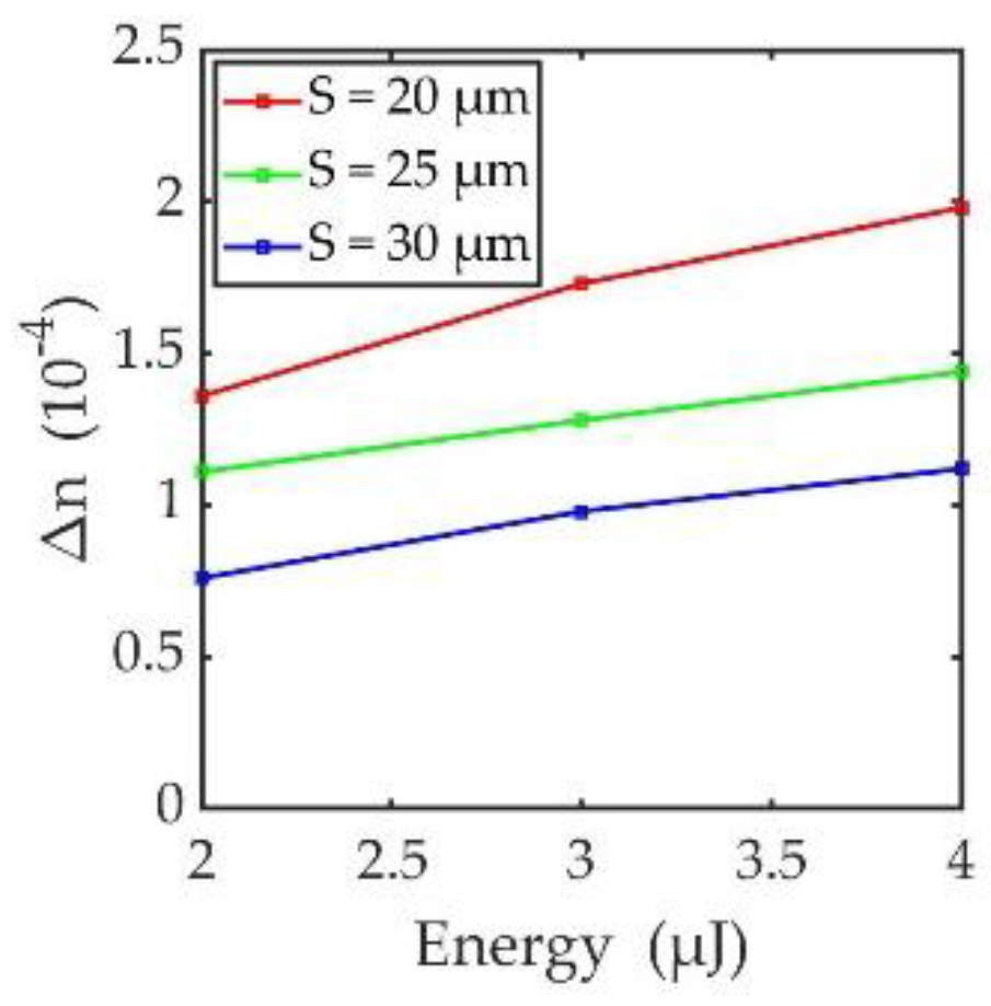
Figure 8 plots the determined , which increases with pulse energy, for all track spacings. This shows that higher pulse energy produces a higher index contrast as more stress is induced inside the crystal.
The propagation loss ( is obtained using Equation (5) and involves subtracting coupling loss (LC) and Fresnel reflection loss (LR) from the measured insertion loss (LI).
The coupling loss between the input beam and the waveguide is determined by the mode field overlap integral [23,24] using Equation (6), where and correspond to the field focused by the microscope objective MO1 and the fundamental guided mode in the waveguide, respectively.
This integral is further simplified to Equation (7) [24,25]. The loss is calculated by using the MFDs of two overlapping modes, i.e.,
where is the MFD of the guide mode, measured at peak intensity. Similarly, is the measured Gaussian beam waist of the focused input beam by objective MO1, in the absence of the waveguide. It may be noted that the absorption loss by optical components (e.g., MO2) needs to be taken into consideration when calculating the propagation loss.
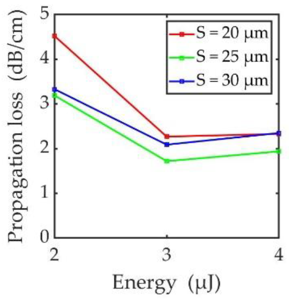
The measured propagation losses for waveguides written at pulse energy values of 2 μJ, 3 μJ, and 4 μJ are shown in Figure 9 for a fixed 100 μm/s scanning speed. The propagation loss first decreases when the input pulse energy is increased from 2 μJ to 3 μJ; it then slightly increases when energy is further increased from 3 μJ to 4 μJ. When the pulse energy is increased, the increase in refractive index contrast provides a better confinement of the mode, which may lead to lower propagation loss; however, structure irregularities may also increase, which increases scattering loss [7]. The tradeoff and balance between these two modifications, which is also dependent on scanning speed, drives the propagation loss shown in Figure 9.
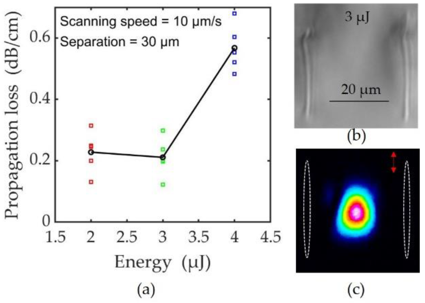
The deposited energy can be controlled by adjusting the scanning speed of the writing process. A lower scanning speed (with a fixed pulse energy) leads to a higher because larger overlap between consecutive pulses allows for larger energy deposition. UPPE simulations show that the energy depletion along the focusing direction varies with input energy of a single pulse. We expect that energy deposition will be affected by scanning speed, since more energy is deposited at a particular location for lower scanning speed, keeping the pulse repetition rate constant. We therefore optimized the fabrication process to minimize the propagation loss for different scanning speeds and track separations. After optimization, a 10 μm/s scanning speed and 30 μm track separation were chosen, leading to different propagation losses at pulse energies of 2 μJ, 3 μJ, and 4 μJ, as shown in Figure 10a. The mean values of propagation loss measured from five samples are 0.23 ± 0.07 dB/cm, 0.21 ± 0.06 dB/cm, and 0.57 ± 0.08 dB/cm at 2 μJ, 3 μJ, and 4 μJ, respectively. This might be caused by the measurement uncertainty due to the coupling sensitivity. Thus, the minimum propagation loss (mean value) achieved through this optimization is 0.21 dB/cm for a waveguide written at a pulse energy of 3 μJ and a scanning speed of 10 μm/s.
Figure 10b shows the transverse cross-section of one of the waveguides written at 3 μJ with a propagation loss of 0.2 dB/cm. The depth of the tracks obtained at 10 μm/s is 28 μm, which is significantly increased from the 15 μm depth obtained at 100 μm/s (Figure 7a). It is noted that there is a slight bending along the track, which has also been reported in other works [5,7,11]. This is possibly caused by the non-optimal stability of the translation stage when used at a low scanning speed, which could be improved with higher-precision hardware. Figure 10c shows the corresponding mode field profile with a diameter of 15.6 μm. The corresponding is 1.83 . The confinement factor is , which indicates better confinement than at a higher scanning speed.
The demonstrated propagation loss (mean), 0.21 dB/cm, is, to the best of our knowledge, much lower than previously reported values (~1 dB/cm) [5,17]. We attribute this low loss to the following two factors. First, in the reported work, a near-infrared wavelength is used to write the tracks, whereas in this work, a 515 nm laser is used. As shown from our UPPE modeling, nonlinear dynamics highly depend on the wavelength-dependent material parameters such as MPI order and MPI cross-section, and, thus, wavelength can play a significant role in modifying crystal structure. Second, optimization under the guidance of UPPE provides a proper combination of scanning speed, track separation, and energy to achieve this lower propagation loss.
4. Conclusions
An extensive UPPE simulation was performed in this work in order to analyze the evolution of pulse energy, fluence, plasma generation, and beam waist along the propagation direction inside silicon and Nd:YAG. The modeling shows that, with increasing input pulse energy, the peak fluence increases and shifts towards the direction from which the beam is coming. Furthermore, the focal volume broadens along the pulse propagation direction. These observations are in good agreement with already reported experimental results in silicon and our experimental observations for Nd:YAG. A detailed experimental study of the effects of pulse energy and scanning speed on the track depth, propagation loss, and modal properties of the waveguides is presented. A minimum (mean) propagation loss of 0.21 ± 0.06 dB/cm is achieved for waveguide configuration written at a scanning speed of 10 μm/s, pulse energy of 3 μJ, and track spacing of 30 μm. The UPPE simulation provides a deeper understanding of the effect of laser parameters on material modification and mode properties during femtosecond laser writing of a waveguide. It can be applied to laser writing in other relevant photonic materials.
Author Contributions
Conceptualization, J.Q. and C.D.; methodology, all authors; experiments, T.F. (primary) and P.K.S.; simulation, T.F., F.R.A.-S., J.Q. and C.D.; investigation, validation and formal analysis, T.F., P.K.S., J.Q. and C.D.; resources, J.Q. and C.D.; data curation, T.F. and P.K.S.; writing—original draft preparation, P.K.S. and T.F.; writing—review and editing, J.Q. and C.D.; supervision, J.Q.; project administration and funding acquisition, J.Q. and C.D.
Funding
This research has been partially funded by award 80NSSC18P2148 from the National Aeronautics and Space Administration Small Business Technology Transfer Program.
Conflicts of Interest
The authors declare no conflict of interest. The funders had no role in the design of the study; in the collection, analyses, or interpretation of data; in the writing of the manuscript, or in the decision to publish the results.
References
- Davis, K.M.; Miura, K.; Sugimoto, N.; Hirao, K. Writing waveguides in glass with a femtosecond laser. Opt. Lett. 1996, 21, 1729–1731. [Google Scholar] [CrossRef] [PubMed]
- Zhang, C.; Dong, N.; Yang, J.; Chen, F.; de Aldana, J.R.V.; Lu, Q. Channel waveguide lasers in Nd: GGG crystals fabricated by femtosecond laser inscription. Opt. Express 2011, 19, 12503–12508. [Google Scholar] [CrossRef] [PubMed]
- Liu, H.; de Aldana, J.R.V.; del Rosal Rabes, B.; Chen, F. Waveguiding microstructures in Nd: YAG with cladding and inner dual-line configuration produced by femtosecond laser inscription. Opt. Mater. 2015, 39, 125–129. [Google Scholar] [CrossRef]
- Siebenmorgen, J.; Calmano, T.; Petermann, K.; Huber, G. Highly efficient Yb: YAG channel waveguide laser written with a femtosecond-laser. Opt. Express 2010, 18, 16035–16041. [Google Scholar] [CrossRef]
- Siebenmorgen, J.; Petermann, K.; Huber, G.; Rademaker, K.; Nolte, S.; Tünnermann, A. Femtosecond laser written stress-induced Nd: Y3Al5O12 (Nd: YAG) channel waveguide laser. Appl. Phys. B 2009, 97, 251. [Google Scholar] [CrossRef]
- Burghoff, J.; Nolte, S.; Tünnermann, A. Origins of waveguiding in femtosecond laser-structured LiNbO3. Appl. Phys. A 2007, 89, 127–132. [Google Scholar] [CrossRef]
- Liu, X.; Qu, S.; Tan, Y.; Zhang, C.; Chen, F. Buried channel waveguides in neodymium-doped KGd(WO4)2 fabricated by low-repetition-rate femtosecond laser writing. Appl. Phys. B 2011, 103, 145–149. [Google Scholar] [CrossRef]
- Chanal, M.; Fedorov, V.Y.; Chambonneau, M.; Clady, R.; Tzortzakis, S.; Grojo, D. Crossing the threshold of ultrafast laser writing in bulk silicon. Nat. Commun. 2017, 8, 773. [Google Scholar] [CrossRef] [PubMed]
- Bharadwaj, V.; Jedrkiewicz, O.; Hadden, J.P.; Sotillo, B.; Vázquez, M.R.; Dentella, P.; Fernandez, T.T.; Chiappini, A.; Giakoumaki, A.N.; Le Phu, T.; et al. Femtosecond laser written photonic and microfluidic circuits in diamond. J. Phys. Photonics 2019, 1, 022001. [Google Scholar] [CrossRef]
- Bharadwaj, V.; Wang, Y.; Fernandez, T.T.; Ramponi, R.; Eaton, S.M.; Galzerano, G. Femtosecond laser written diamond waveguides: A step towards integrated photonics in the far infrared. Opt. Mater. 2018, 85, 183–185. [Google Scholar] [CrossRef] [Green Version]
- Sotillo, B.; Bharadwaj, V.; Hadden, J.P.; Sakakura, M.; Chiappini, A.; Fernandez, T.T.; Longhi, S.; Jedrkiewicz, O.; Shimotsuma, Y.; Criante, L.; et al. Diamond photonics platform enabled by femtosecond laser writing. Sci. Rep. 2016, 6, 35566. [Google Scholar] [CrossRef] [PubMed]
- Panusa, G.; Pu, Y.; Wang, J.; Moser, C.; Psaltis, D. Photoinitiator-free multi-photon fabrication of compact optical waveguides in polydimethylsiloxane. Opt. Mater. Express 2019, 9, 128–138. [Google Scholar] [CrossRef]
- Chen, F.; de Aldana, J.V. Optical waveguides in crystalline dielectric materials produced by femtosecond-laser micromachining. Laser Photonics Rev. 2014, 8, 251–275. [Google Scholar] [CrossRef]
- Ródenas, A.; Torchia, G.A.; Lifante, G.; Cantelar, E.; Lamela, J.; Jaque, F.; Roso, L.; Jaque, D. Refractive index change mechanisms in femtosecond laser written ceramic Nd:YAG waveguides: Micro-spectroscopy experiments and beam propagation calculations. Appl. Phys. B 2009, 95, 85–96. [Google Scholar] [CrossRef]
- Okhrimchuk, A. Femtosecond fabrication of waveguides in ion-doped laser crystals. In Coherence and Ultrashort Pulse Laser Emission; IntechOpen: London, UK, 2010. [Google Scholar]
- Calmano, T.; Siebenmorgen, J.; Hellmig, O.; Petermann, K.; Huber, G. Nd: YAG waveguide laser with 1.3 W output power, fabricated by direct femtosecond laser writing. Appl. Phys. B 2010, 100, 131–135. [Google Scholar] [CrossRef]
- Li, S.-L.; Ye, Y.-K.; Wang, M.-W. Femtosecond laser written channel optical waveguide in Nd: YAG crystal. Opt. Laser Technol. 2014, 58, 89–93. [Google Scholar] [CrossRef]
- Kolesik, M.; Moloney, J.V. Nonlinear optical pulse propagation simulation: From Maxwell’s to unidirectional equations. Phys. Rev. E 2004, 70, 036604. [Google Scholar] [CrossRef]
- Itina, T.E.; Mamatkulov, M.; Sentis, M.L. Nonlinear fluence dependencies in femtosecond laser ablation of metals and dielectric materials. Opt. Eng. 2005, 44, 051109. [Google Scholar] [CrossRef]
- Zavedeev, E.; Kononenko, V.; Konov, V. Delocalization of femtosecond laser radiation in crystalline Si in the mid-IR range. Laser Phys. 2015, 26, 016101. [Google Scholar] [CrossRef]
- Polynkin, P.; Kolesik, M. Critical power for self-focusing in the case of ultrashort laser pulses. Phys. Rev. A 2013, 87, 053829. [Google Scholar] [CrossRef]
- Darginavičius, J.; Majus, D.; Jukna, V.; Garejev, N.; Valiulis, G.; Couairon, A.; Dubietis, A. Ultrabroadband supercontinuum and third-harmonic generation in bulk solids with two optical-cycle carrier-envelope phase-stable pulses at 2 μm. Opt. Express 2013, 21, 25210–25220. [Google Scholar] [CrossRef] [PubMed]
- Liang, A.; Hu, L.; Liang, Z. Mode-field-diameter and the coupling loss between inner and outer segment of photoreceptors. Opt. Photonics J. 2015, 5, 151. [Google Scholar] [CrossRef]
- Fan, C.; Liang, A. Splice loss between different Gaussian-elliptic-field single-mode fibers. J. Lightwave Technol. 1990, 8, 173–176. [Google Scholar] [CrossRef]
- Nemoto, S.; Makimoto, T. Analysis of splice loss in single-mode fibres using a Gaussian field approximation. Opt. Quantum Electron. 1979, 11, 447–457. [Google Scholar] [CrossRef]
Figure 1.
UPPE simulation for silicon: evolution of (i) pulse energy, (ii) fluence, and (iii) plasma density along the propagation direction of a laser pulse for different (a) input energy, and (b) numerical aperture (NA) of the focusing optics.
Figure 1.
UPPE simulation for silicon: evolution of (i) pulse energy, (ii) fluence, and (iii) plasma density along the propagation direction of a laser pulse for different (a) input energy, and (b) numerical aperture (NA) of the focusing optics.

Figure 2.
Beam waist evolution for silicon (a) at different pulse energy for 0.5 NA and (b) for different NA values at 50 nJ input pulse energy.
Figure 2.
Beam waist evolution for silicon (a) at different pulse energy for 0.5 NA and (b) for different NA values at 50 nJ input pulse energy.

Figure 3.
Energy and fluence evolution along the beam propagation direction in Nd:YAG.

Figure 4.
Beam waist evolution due to self-focusing and defocusing in Nd:YAG.

Figure 5.
Schematic of the waveguide writing setup. Legend: MO, microscope objective.

Figure 6.
Schematic of the waveguide characterization set up.

Figure 7.
(a) Cross-section of the waveguide tracks and (b) near-field fluence maps of the guided modes at the three input energy values of 2 μJ, 3 μJ, and 4 μJ.
Figure 7.
(a) Cross-section of the waveguide tracks and (b) near-field fluence maps of the guided modes at the three input energy values of 2 μJ, 3 μJ, and 4 μJ.

Figure 8.
Refractive index contrast as a function of pulse energy; the scanning speed is 100 μm/s for all cases.
Figure 8.
Refractive index contrast as a function of pulse energy; the scanning speed is 100 μm/s for all cases.

Figure 9.
Propagation loss of waveguides fabricated at different pulse energies and track separation, for a scanning speed equal to 100 μm/s.
Figure 9.
Propagation loss of waveguides fabricated at different pulse energies and track separation, for a scanning speed equal to 100 μm/s.

Figure 10.
(a) Propagation loss versus energy for waveguides written at 10 μm/s speed and 30 μm separation. The black curve represents the mean value of propagation loss, whereas the red, green, and blue squares represent the individual propagation loss values at 2 μJ, 3 μJ, and 4 μJ pulse energy values, respectively. (b) Transverse cross-section of one of the waveguides written at 3 μJ. (c) Guided mode profile corresponding to the waveguide shown in (b). The mode field diameter is 15.6 μm.


Table 1.
Silicon parameters used for unidirectional pulse propagation equation (UPPE) simulation.
| Parameter | Value |
|---|---|
| Energy gap | 1.12 eV |
| Multi-photon ionization (MPI) order | 2 (@1.3 μm) |
| Nonlinear coefficient | 1.5 × 10⁻¹⁸ m2/W |
| Neutral density | 5 × 1028 m−3 |
| Collision time | 3.3 fs |
| MPI cross-section | σ2 = 5.23 × 10⁻²² m4/W2s |
Table 2.
Nd:Y3Al5O12 (Nd:YAG) parameters used for UPPE simulation.
| Parameter | Value |
|---|---|
| Energy gap | 6.5 eV |
| MPI order | 11 (@2 μm) |
| Nonlinear coefficient | 7 × 10⁻²⁰ m2/W |
| Neutral density | 7 × 1028 m−3 |
| Collision time | 3 fs |
| MPI cross-section | σ11 = 2 × 10−181 m4/W2s |
© 2019 by the authors. Licensee MDPI, Basel, Switzerland. This article is an open access article distributed under the terms and conditions of the Creative Commons Attribution (CC BY) license (http://creativecommons.org/licenses/by/4.0/).
Share and Cite
MDPI and ACS Style
Feng, T.; Sahoo, P.K.; Arteaga-Sierra, F.R.; Dorrer, C.; Qiao, J. Pulse-Propagation Modeling and Experiment for Femtosecond-Laser Writing of Waveguide in Nd:YAG. Crystals 2019, 9, 434. https://0-doi-org.brum.beds.ac.uk/10.3390/cryst9080434
AMA Style
Feng T, Sahoo PK, Arteaga-Sierra FR, Dorrer C, Qiao J. Pulse-Propagation Modeling and Experiment for Femtosecond-Laser Writing of Waveguide in Nd:YAG. Crystals. 2019; 9(8):434. https://0-doi-org.brum.beds.ac.uk/10.3390/cryst9080434
Chicago/Turabian StyleFeng, Tao, Pankaj K. Sahoo, Francisco R. Arteaga-Sierra, Christophe Dorrer, and Jie Qiao. 2019. "Pulse-Propagation Modeling and Experiment for Femtosecond-Laser Writing of Waveguide in Nd:YAG" Crystals 9, no. 8: 434. https://0-doi-org.brum.beds.ac.uk/10.3390/cryst9080434
Note that from the first issue of 2016, this journal uses article numbers instead of page numbers. See further details here.