Article

An Integrated Photonic Electric-Field Sensor Utilizing a 1 × 2 YBB Mach-Zehnder Interferometric Modulator with a Titanium-Diffused Lithium Niobate Waveguide and a Dipole Patch Antenna

Department of Electronic and Electrical Fusion Engineering, Hongik University, Sejong 30016, Korea
Submission received: 29 July 2019 / Revised: 22 August 2019 / Accepted: 31 August 2019 / Published: 2 September 2019
(This article belongs to the Special Issue Recent Progress in Lithium Niobate)

Abstract

:
We studied photonic electric-field sensors using a 1 × 2 YBB-MZI modulator composed of two complementary outputs and a 3 dB directional coupler based on the electro-optic effect and titanium diffused lithium–niobate optical waveguides. The measured DC switching voltage and extinction ratio at the wavelength 1.3 μm were ~16.6 V and ~14.7 dB, respectively. The minimum detectable fields were ~1.12 V/m and ~3.3 V/m, corresponding to the ~22 dB and ~18 dB dynamic ranges of ~10 MHz and 50 MHz, respectively, for an rf power of 20 dBm. The sensor shows an almost linear response to the applied electric-field strength within the range of 0.29 V/m to 29.8 V/m.

1. Introduction

Electric-field sensors that exhibit wide, flat frequency response characteristics are important tools for electromagnetic compatibility and interference (EMC/EMI) measurements, high-frequency electronic circuit analysis, medical equipment field observation, radio-frequency reception, and high-power microwave detection. The importance of these sensors is increasing as mobile multimedia communications develops [1,2]. It is necessary to accurately evaluate the strength and distribution of electromagnetic fields surrounding electronic equipment to estimate electromagnetic compatibility. The requirements for electric-field sensors based on the important applications mentioned above are as follows: their wide frequency bandwidth and large dynamic range; their high spatial resolution and low interference to the original field; and their high stability and accuracy.
Even though a variety of sensing modules have been developed, those with photonic links reduce or eliminate some of the inaccuracies and systematic errors that affect measurement techniques using conventional EM-field sensors. They provide electrical isolation, which eliminates ground loops and common-mode electrical pickup between the sensor head and the electronics module. Moreover, the optical fibers and dielectric components produce minimal field distortion. In addition, they can preserve both the phase and amplitude of high-frequency fields with good fidelity and low losses. The development of optical-fiber and optoelectronic components for the telecommunications industry has made it possible to implement photonic sensors that are accurate and convenient to use.
In particular, titanium-diffused lithium niobate (Ti: LiNbO3) waveguide devices are suitable for electric-field detection since their sensors will not perturb the field to be measured. A linear modulator that is passively biased to the optimal linear operating point is required. This has been demonstrated for asymmetric Mach–Zehnder interferometers (MZIs) and 1 × 2 directional couplers. The former devices have an intrinsic bias of π/2, where a geometrical path length difference of a quarter of a wavelength is required between the two arms [3,4,5,6,7]. However, it is not easy to obtain optimal operation through path length difference alone, because of fabrication tolerances.
Moreover, the latter device is automatically biased to the optimal 3 dB operating point due to its symmetrical structure, and it provides a greater tolerance in the fabrication process than an asymmetric Mach–Zehnder interferometric optical modulator [8,9,10,11]. However, the complexity of the transfer function makes it impossible to utilize the sensor in a specific range (namely, the ratio of interaction length to conversion length).
In contrast, a Y-fed balanced-bridge MZI modulator (YBB-MZI) consists of a 3 dB coupler at the output, with two complementary output waveguides [12,13,14,15,16,17,18,19]. This type of modulator provides a well-defined transfer function for the output optical power versus the detected electric-field intensity and can be automatically biased at the optimum 3 dB operating point due to its symmetrical structure, which offers a more tolerant design in the fabrication process than Mach–Zehnder interferometric modulators or 1 × 2 directional couplers, which are asymmetrical. A mono-shield gold electrode structure was applied in YBB-MZI by the Tsinghua University group to detect a very high electric field [12]. Moreover, the minimum electric-field strength that can be sensed is determined by the relative intensity noise (RIN) of the laser diode. Therefore, a YBB-MZI configuration was proposed by a German group to reduce RIN and improve sensitivity with a balanced optical receiver [16].
In this paper, we provide the quantitative theory of a YBB-MZI modulator and report on a fabricated Ti: LiNbO3 YBB-MZI modulator operating at a 1.3 μm wavelength. We also present, in detail, the fabrication process and design parameters, as well as the optical and electrical performances of a packaged electric-field sensor with a diploe patch antenna, including the minimum detectable electric-field intensity, dynamic range, and sensitivity.

2. Theory, Fabrication, and Performance of a Ti: LiNbO3 YBB-MZI Modulator
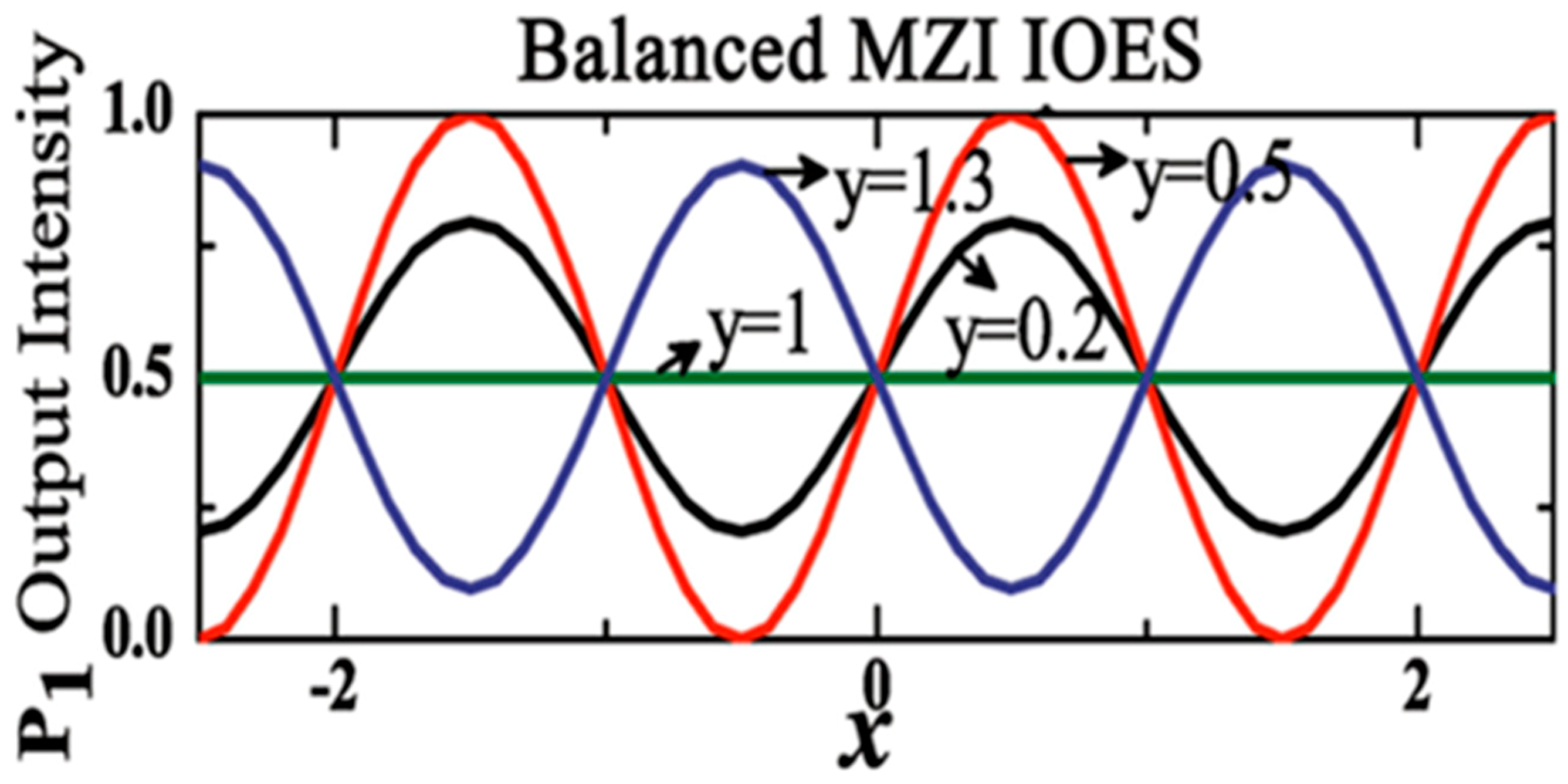
2.1. Device Theory

The YBB-MZI modulator consists of a 3 dB directional coupler at the output and has two complementary output waveguides, as shown in Figure 1. A dipole patch antenna was placed around the arm of the MZI structure to detect the electric field.
The operating characteristics of a 2 × 2 directional coupler are represented by the coupling length Lc, the coupling coefficient κ, and the wavenumber β of the waveguide. If the transmission loss is ignored, the transfer matrix of a directional coupler is expressed by [20]:
( E 01 ¯ E 02 ¯ ) = e i β L c ( c o s   κ L c j   s i n   κ L c j   s i n   κ L c c o s   κ L c ) ( E i 1 ¯ E i 2 ¯ ) .
where Ei1, Ei2, and E01, E02 are the input and output optical modes, respectively. The incident single-mode optical-wave is equally divided in two by a 3 dB power splitter located at the input stage and can be expressed as follows:
E i 1 ¯ ,   E i 2 ¯ =   1 2 e j θ
where θ is the initial phase.
The dipole patch antenna with an electrode, as shown in Figure 1b, creates an electric field on one of the two arms of the MZI, which eventually induces a change of the refractive index and an unbalanced modulation. Before going into the output directional coupler, the optical wave in the two arms has an extrinsic phase mismatch Φ ( E e ) due to the detected electric field. This phase mismatch Φ ( E e ) can be expressed as
Φ ( E e ) = ± π λ n e 3 γ 33 Γ l e E e
where le is the length of the electrode connected to the dipole patch antenna, r33 is the electro-optic coefficient of lithium niobate (~30 pm/V), λ is the optical wavelength, ne is the extraordinary refractive index of lithium niobate, Ee is the electric-field strength through the waveguide, and Γ (0 < Γ < 1) is the overlap integral between the applied electrical field and the optical wave. Therefore, the optical-wave going into the output coupler can be represented as
E ¯ i 1 = 1 2 e j ( θ + Φ ( E e ) )
E ¯ i 2 = 1 2 e j θ .
Combining (1) with (4), the output power of the YBB-MZI modulator is expressed as
P 01 = 1 2 [ 1 + s i n ( π y ) · s i n ( π x ) ] = 1 2 [ 1 + s i n ( 2 k L c ) · s i n ( Φ ( E e ) ) ]
P 02 = 1 2 [ 1 s i n ( π y ) · s i n ( π x ) ] = 1 2 [ 1 s i n ( 2 k L c ) · s i n ( Φ ( E e ) ) ]
where x = Φ ( E e ) / π is the normalized phase-mismatch, y = L c / l c is the normalized coupling length, and l c = π / 2 k is the coupling conversion length.
The output intensity Po1 is simulated and plotted for the YBB-MZI electric-field sensor, as shown in Figure 2. The YBB-MZI sensor shows a sinusoidal transfer function for different y-values. The value of y only affects the extinction ratio, which can be represented as sin( π y ). For most cases (where sin( π y ) ≠ 0), the transfer function is acceptable as the extinction ratio only impacts the E-field measurement sensitivity. To support the maximum sensitivity, the coupling length should satisfy the condition
s i n ( 2 k · L c ) = 1 ,
where k · L c = ( 2 n + 1 ) π 4 , (   n = 0 ,   1 ,   2 , )   .

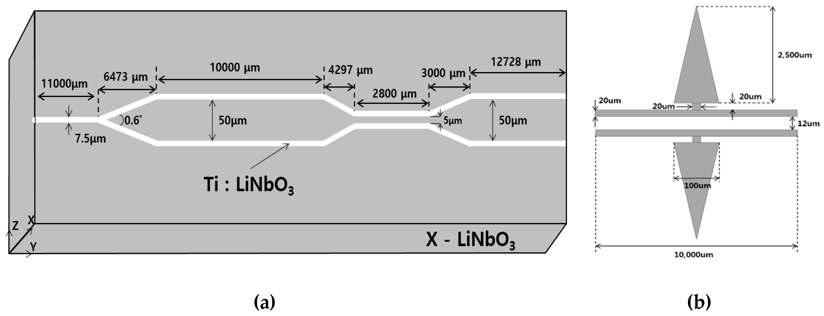
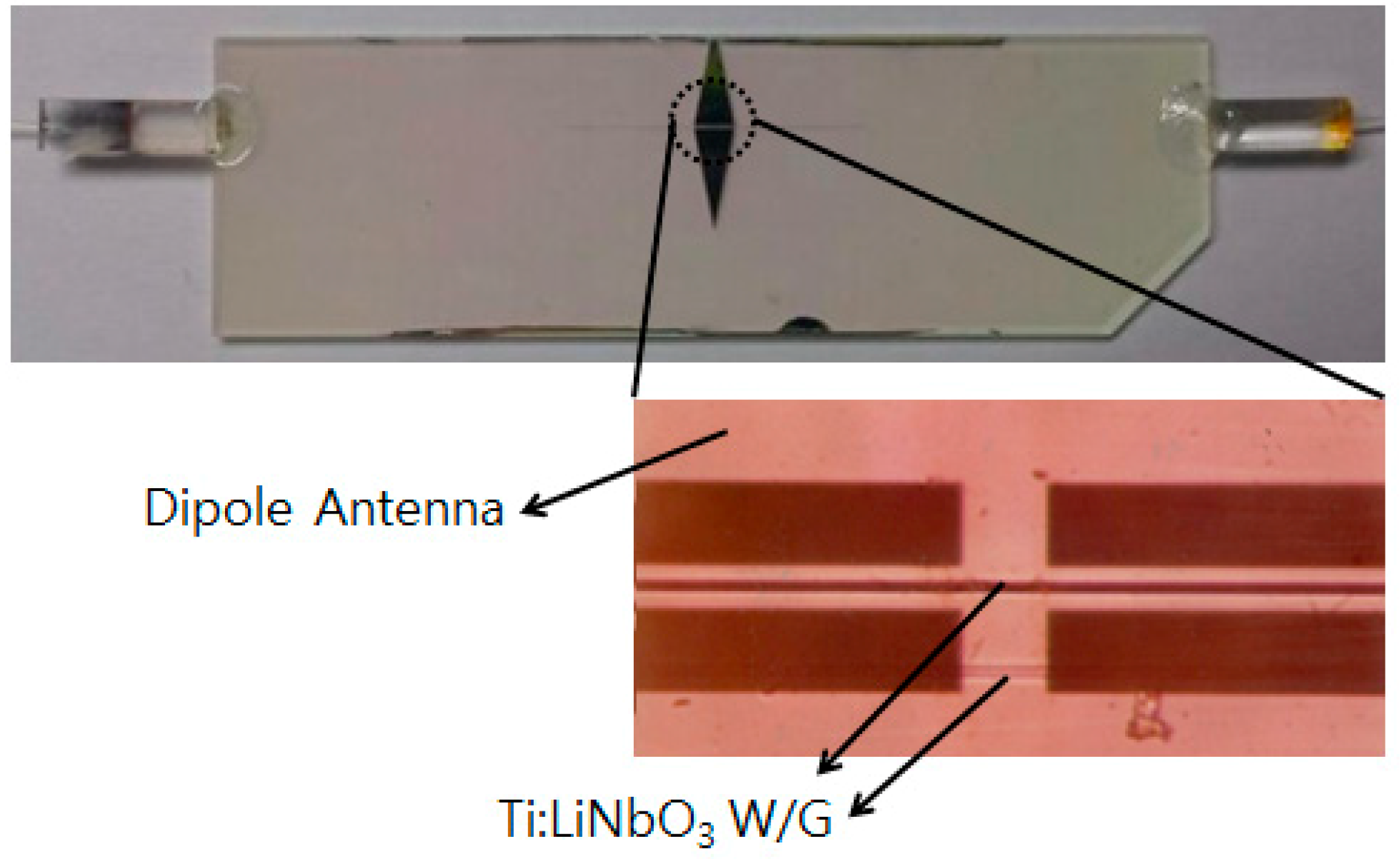
2.2. Designs and Fabrication

Using single-mode Ti:LiNbO3 channel waveguides, a symmetric 1 × 2 YBB-MZI modulator with a dipole patch antenna was designed for operation at a wavelength of ~1.3 μm in an x-cut, y-propagating LiNbO3 substrate, as shown in Figure 1. The device consists of a Y-branch splitter, a phase modulator, and a directional coupler. The entire device’s structure is similar to that of a Mach–Zehnder interferometer with two output ports. The waveguide width is 7.5 μm for single-mode operation, and the splitting angle of the Y-branch is 0.6° for decreasing the propagation loss as low as possible and for fabrication tolerance. The gap interval between the two adjacent waveguides of the directional coupler and the parallel coupling length are 5 μm and 2.8 mm, respectively, to split the optical power equally into two output channels with a nominal coupling constant-length product, κ∙Lc of π/4. The interval between the inner edges of the two output waveguides is 50 μm, thereby preventing optical power coupling between the two output channels. As shown in Figure 1b, the gap and length of the modulation electrode connected to the dipole patch antenna are 12 μm and 10 mm, respectively. The results of the BPM-CAD 3D simulation of the optical wave propagating through the YBB-MZI modulator are shown in Figure 3 [21]. When no voltage was applied, the two intensity profiles were approximately identical, with ~1% or lower accuracy because of the nearly equal intensity splitting, as shown in Figure 3a. Therefore, the YBB-MZI modulator was intrinsically set at the 3 dB half-power point. While the driving voltage increased to 5 V and 10 V, the light in the lower branch of the device was coupled with the upper branch, where the light intensity of the lower branch decreased and the intensity of the upper branch increased, as shown in Figure 3b,c. When 10 V was applied, the light of the lower branch almost disappeared, and the light intensity of the upper branch reached the highest level. Therefore, it could be theoretically confirmed that the switching voltage required to modulate the light intensity of either branch from a bar state (maximum intensity) to a cross state (minimum intensity) was ~10 V.
An investigation of the formation of optical waveguides in LiNbO3 by metal ion diffusion indicated an increase or decrease in the refractive index depending on the valence of the in-diffused ion. Higher-valence ions such as Ti3+, Fe3+, and Cr3+ increase both the ordinary and extraordinary indices. It appears that lower-valence ions replace Li+ sites, while higher-valence ions replace Nb5+ sites. Experimental results indicated that the in-diffused Ti metal in LiNbO3 was all tetravalent (i.e., Ti atoms are fully ionized). There are no electrons in particularly filled d-orbitals to absorb the electromagnetic energy at visible wavelengths. This explains the measurement of low losses of waveguides fabricated by Ti diffusion into LiNbO3 [22,23,24]. The dominant sources of waveguide loss are scattering from LiNbO3 surface imperfections due to diffusion and possibly absorption by the metal ions.
The 1 × 2 YBB-MZI waveguide structure, as shown in Figure 1a, was fabricated on an x-cut, 3-inch, 1-mm-thick LiNbO3 wafer as the substrate using UV photolithography and thermal diffusion. First, a 1050-Å-thick Ti-film on the LiNbO3 substrate was deposited by an e-beam evaporator, and then the desired Ti-film patterns with 7.5 μm widths were formed by photolithography and the wet-etching process, followed by thermal diffusion for 8 hours at 1050 °C in wet-ambient. The resulting Ti-diffused channel waveguides grew to a thickness two or three times that of the Ti-film stripe. Such surface growth makes it easy to observe Ti-diffused waveguides with a microscope, as shown in Figure 4. Furthermore, the diffused waveguide has Gaussian index profiles in its depths. The effective index increases in linear proportion to the Ti film’s thickness. This feature indicates that the propagation constant of the fundamental mode can easily be controlled by changing the film thickness alone.
The waveguide edges were optically polished to allow butt-coupling and pig-tailing. A silicon dioxide buffer layer with a thickness of ~3000 Å was deposited on the substrate using an electron beam and 99.99% pure SiO2 pellets to reduce the propagation loss due to the absorption of the light wave of the antenna’s metal. An aluminum dipole patch antenna and electrode ~5000 Å thick (as shown in Figure 1b) were formed along one of the two arms of the YBB-MZI to allow sensing of the electric field. A polarization-maintaining single-mode optical fiber and multi-mode fiber were attached to the input and output waveguides, respectively. Figure 4 shows a photograph of the implemented device with the attached optical fibers and a dipole patch antenna. The insertion loss of the device, including the input/output fiber, was measured to be about 11.7 dB, which includes the fiber-connector loss, pig-tailing loss, mode-mismatch loss, and propagation loss of the waveguides.

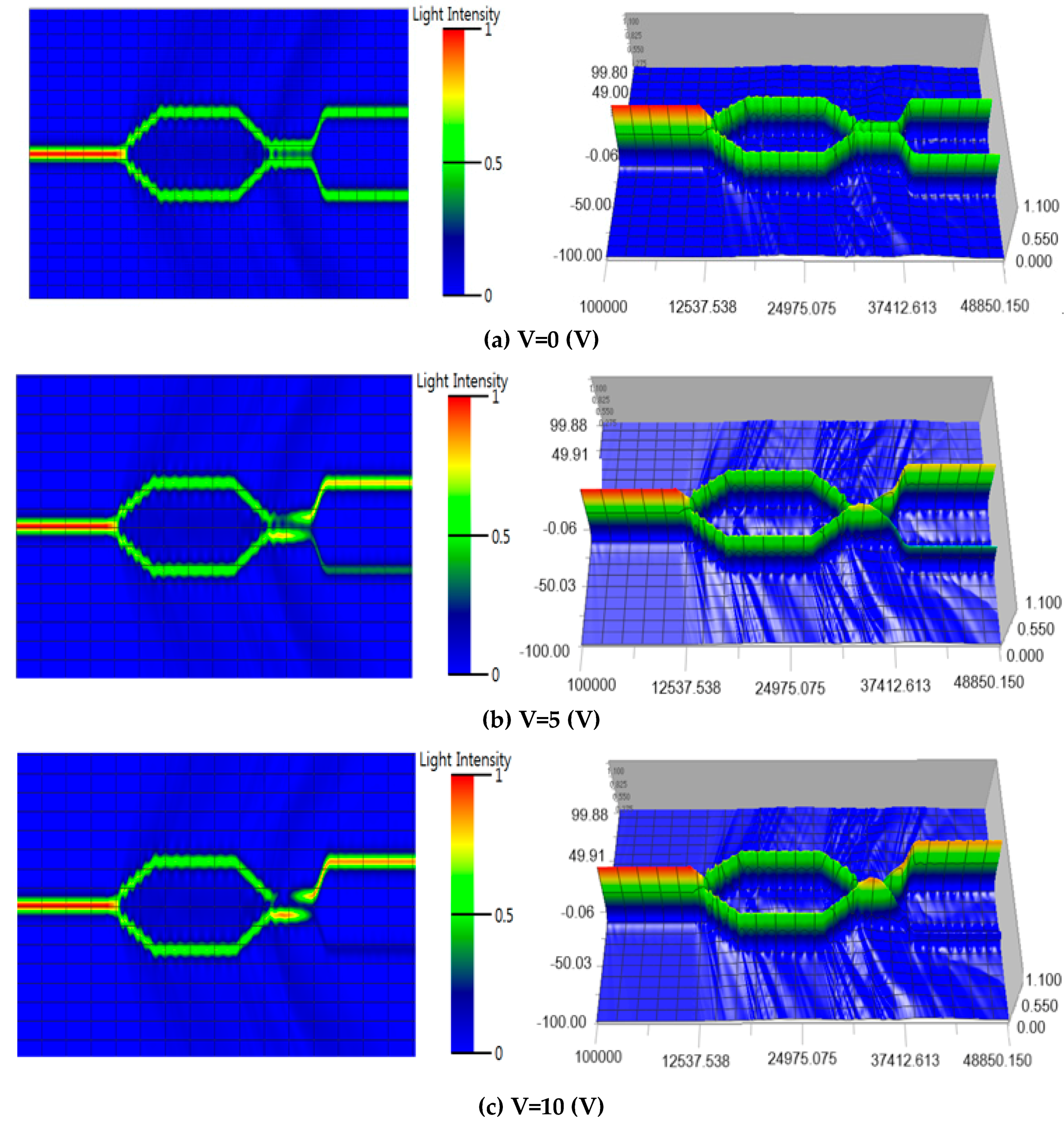
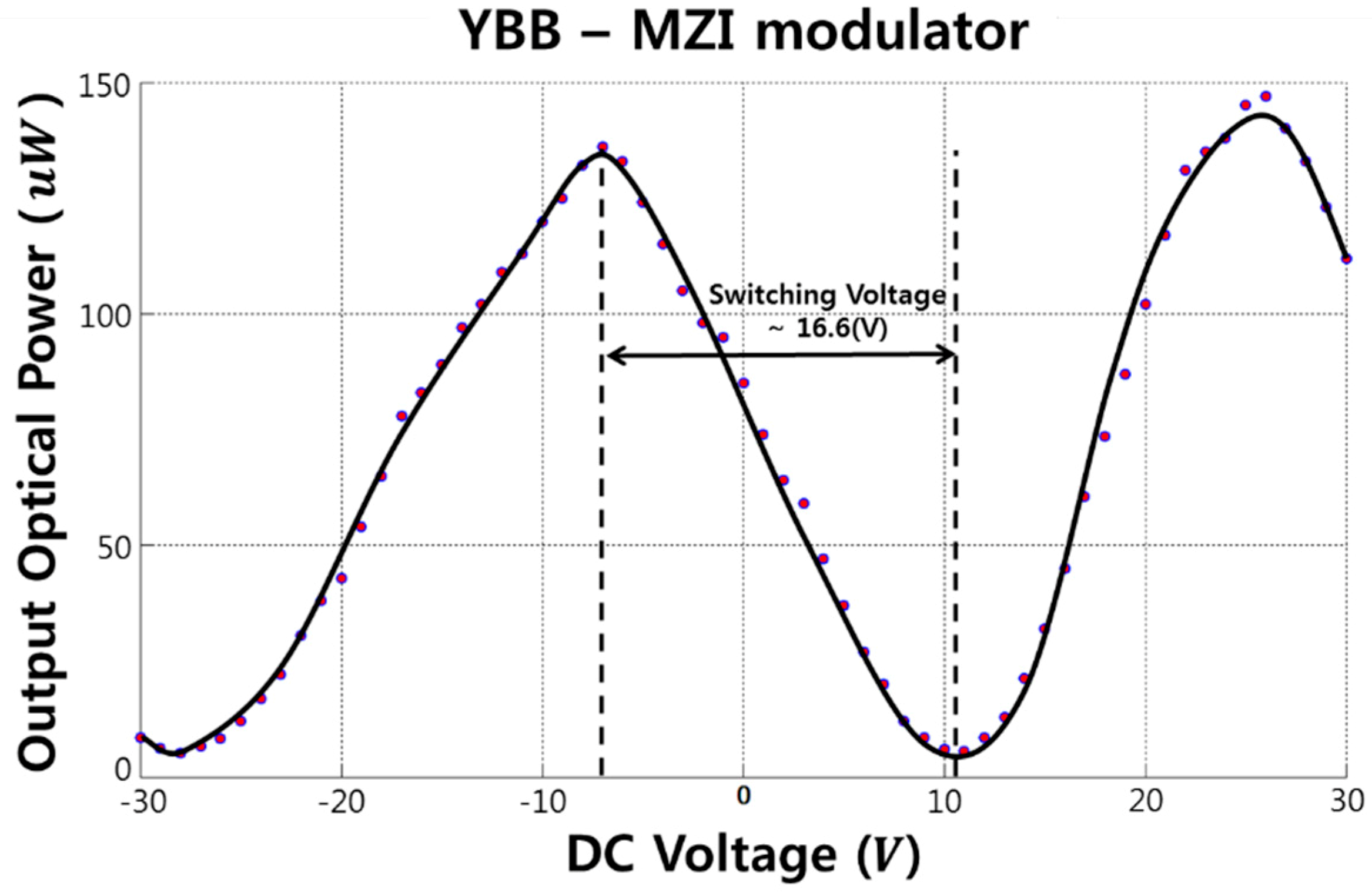
2.3. Performance Evaluations

The fabricated device without an attached optical fiber was first tested by applying DC voltages. The device’s performance and characterization were observed using a tunable laser with butt-coupling at a wavelength of 1.3. The TE-polarized input light was butt-coupled to the devices, collected at the output by a microscope’s objective lens, and focused onto a photo-detector for measurement. TE or TM polarized light was selected by properly adjusting a fiber optic polarization controller. We first observed the single-mode propagation for TE polarization in the 1 × 2 YBB-MZI modulator.
It was observed that when the voltage was not applied, the two outputs of the device were almost the same. The voltage required to switch either output light power from a bar state (maximum intensity) to a cross state (minimum intensity) was measured to be ~-16.6 V, which corresponds to a ~14.7 dB extinction ratio. Figure 5 shows the optical output power versus the DC voltage measured by an optical power meter and shows a slightly asymmetric DC output characteristic, as well as a switching voltage of ~16.6 V, as mentioned previously. The AC modulation responses of the two outputs versus the driving sinusoidal voltage were further measured in Figure 6, where the optical signals are below the sinusoidal curve and the applied ac voltage signal is above the curve, at a frequency of ~1 kHz (5 V/div). The power of the two outputs was confirmed to be nearly equal, and the periodic exchange of output power in the two outputs expresses a good inverse relationship in the output sinusoidal curves. The slightly skewed and flattened shape in the optical response in Figure 6 was observed due to the imperfect single mode waveguide and the out-diffusion that occurred in the diffusion process.

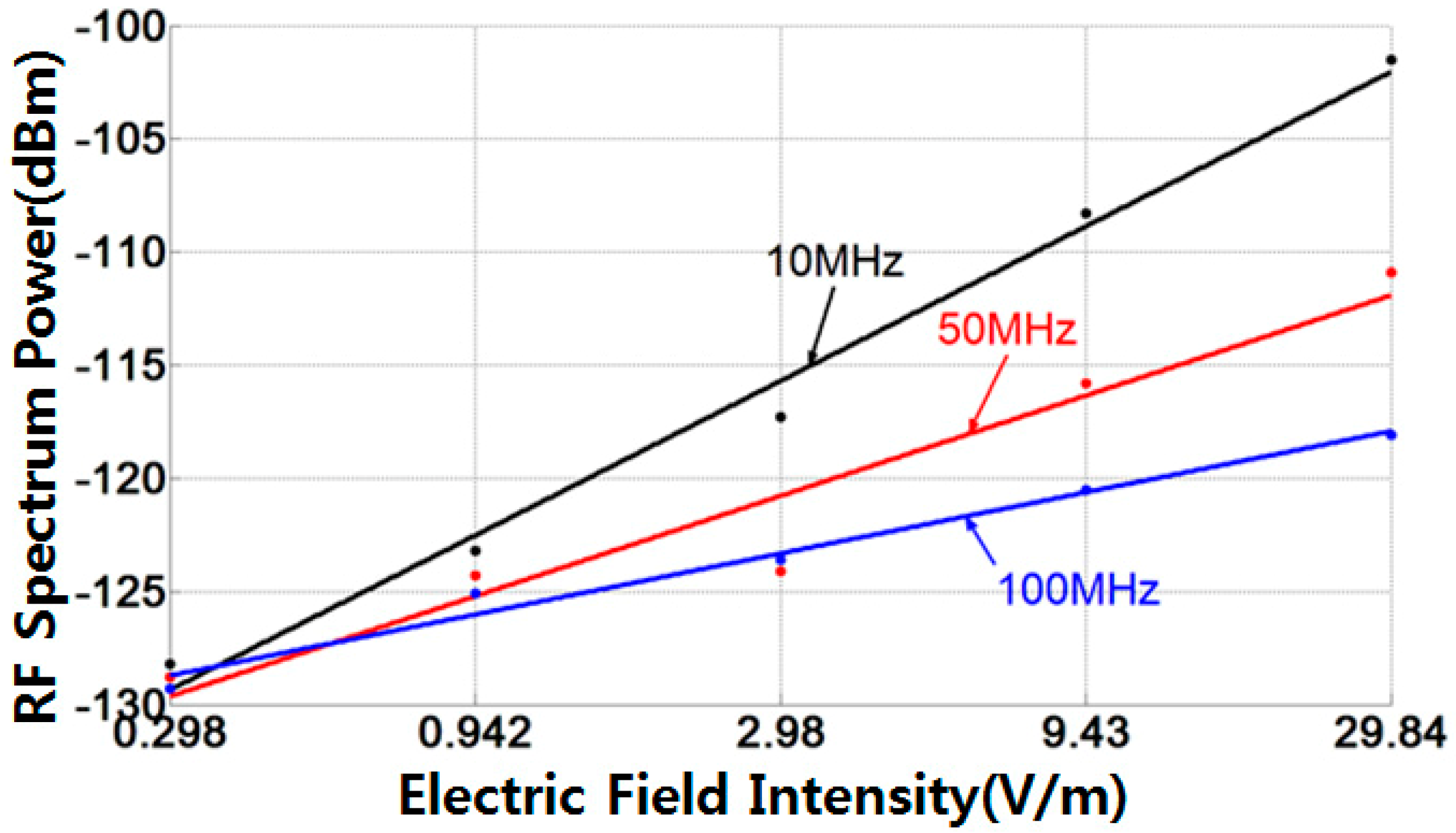
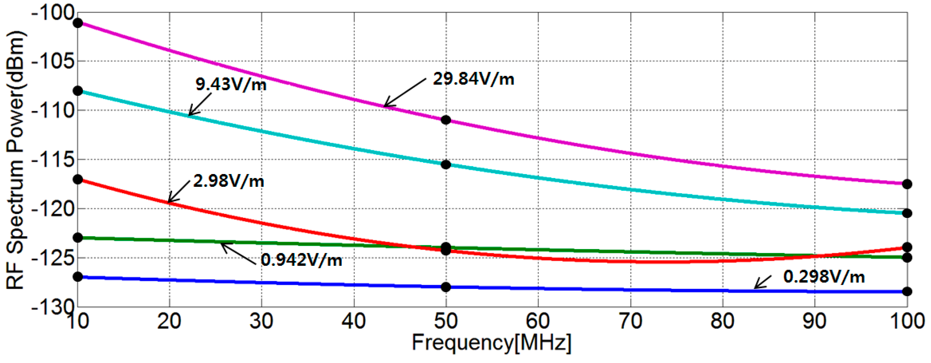
3. Measurement and Experimental Results

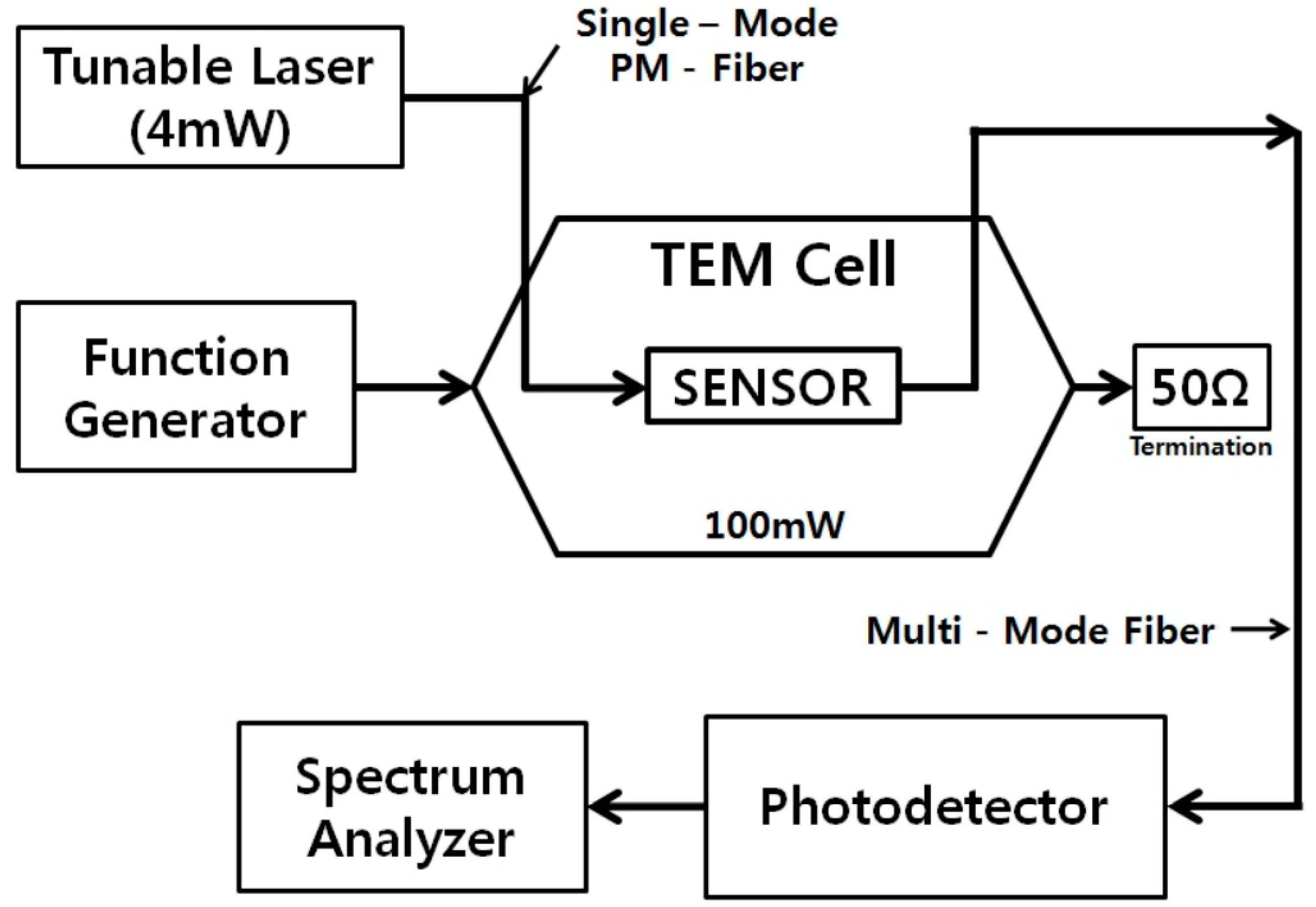
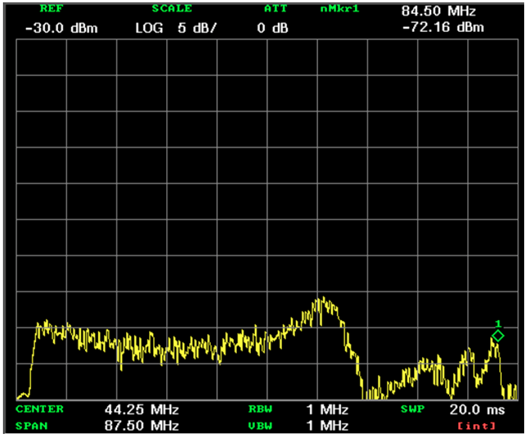
3.1. Experimental Setup

To measure the frequency responses and the minimum measurable field strength of the device, frequency tests were performed utilizing a tunable laser at a wavelength of 1.3 μm. The input optical power was about 1.4 mW. A detailed diagram of the measurement setup is shown in Figure 7. The device was tested in a uniform electric-field environment by placing it in a Transverse Electro Magnetic (TEM) cell (Tescom TC-5010A), as shown in Figure 7, where the TEM cell is utilized to generate accurate electro-magnetic (EM) waves over a wide frequency range. EM waves generated in the cell are transmitted in the transverse mode and have similar characteristics to the plane-wave. The optical fibers penetrating through the slanted wall of the TEM cell and were connected to the laser and photodetector using an FC/PC fiber-optic connector. The applied electric-field strength was calculated using the output level and the size of the TEM cell. The −20~+20 dBm (10 μW~100 mW) rf input power to the TEM cell corresponds to the electric-field strength from 0.293 V/m to 23.2 V/m. Due to the high permittivity (ε ≈ 35) of LiNbO3, the substantial electric-field intensity experienced on the sensor substrate (23.2 V/m) corresponds to 0.66 V/m in the TEM cell. The rf power propagates through the TEM cell in the same direction as the light passing through the optical fibers and the sensor [9].

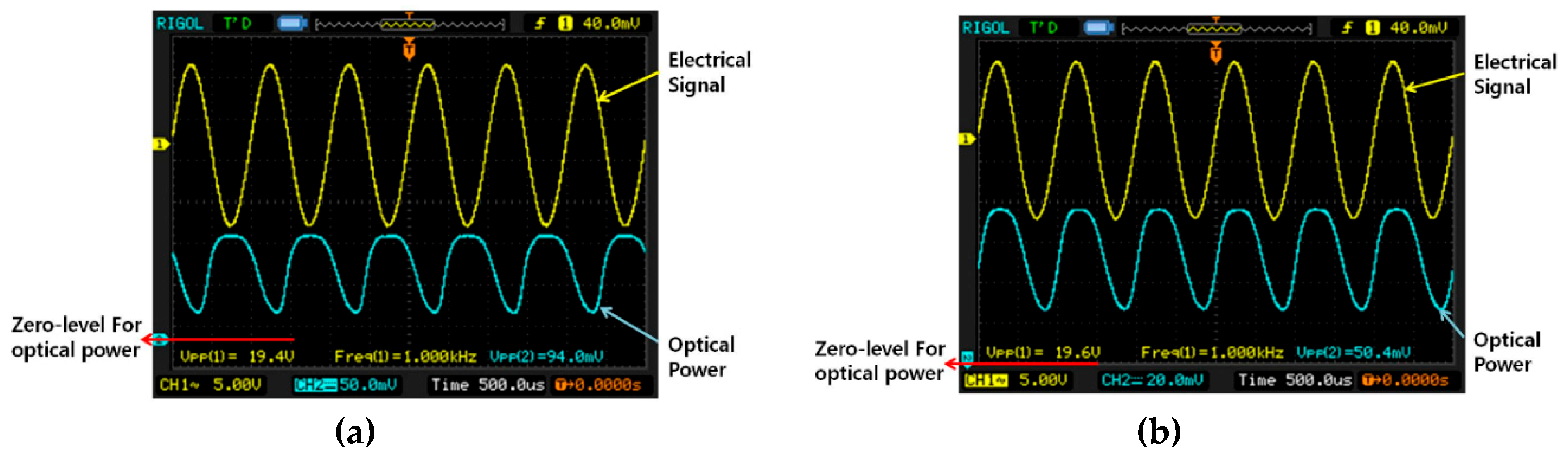
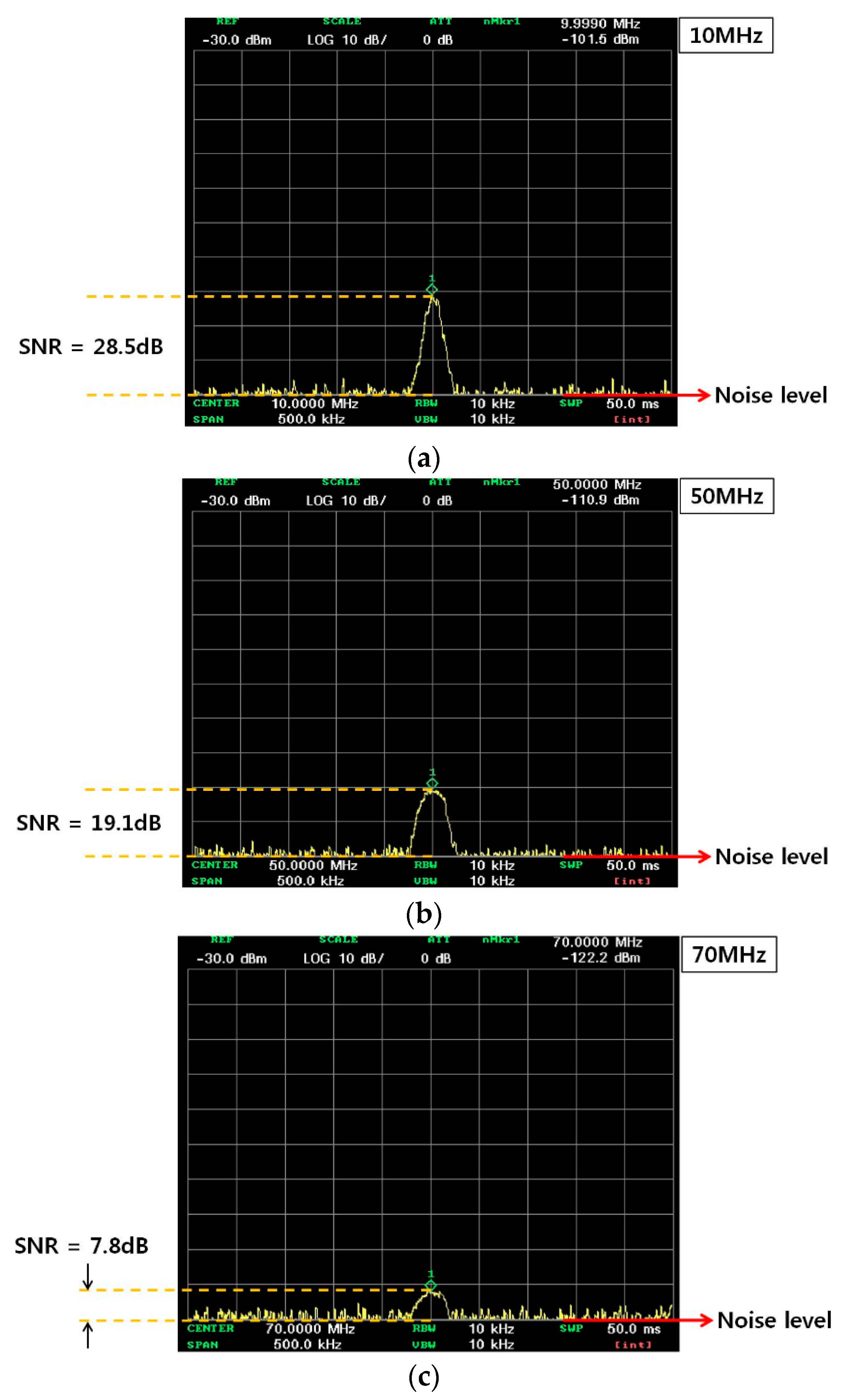
3.2. Test Results and Discussions

Figure 8 shows the spectrum-analyzer outputs for an input of 20 dBm to the TEM cell at frequencies of 10, 50, and 70 MHz, respectively. The rf power detected at the photodetector was measured to be −101.5, −110.9, and −122.2 dBm, as shown in Figure 8, and the noise floor was measured to be about −130 dBm at the same frequencies. The internal electric field of 29.8 V/m in the TEM cell produced an SNR of 28.5, 19.1, and 7.8 dB at each frequency. Therefore, the minimum detectable electric-fields are ~1.12, ~3.3, and ~12.13 V/m, respectively, at those three frequencies, based on the equation Emin = 29.8 × 10(-SNR/20) V/m.
Figure 9 shows the sensitivity curves at rf frequencies of 10 MHz, 50 MHz, and 100 MHz. We can confirm that the graph shows almost linear response characteristics from the applied electric-field intensity from 0.293 V/m to 23.2 V/m. Even though some data are off the linear response line, they remain very close. The device also shows a dynamic range of about ~22, ~18, and ~12 dB at frequencies of 10, 50, and 100 MHz, respectively. Figure 10 shows the photodetector power at different electric-field intensities.
Figure 11 illustrates the frequency response of the sensor measured with 20 dBm of rf input power applied to the TEM cell. This figure shows a nearly flat frequency response from 1 MHz to ~50 MHz. The cut-off high frequency of the device is derived from the series-coupled time constant of the electrode resistance and the structural and packaged capacitances of the device. Therefore, a much higher cutoff frequency can be expected when a metal material with a higher coefficient of conductivity, such as gold instead of aluminum, is applied to an electrode.
So far, the theoretical analysis and experimental results have confirmed that an electric-field sensor based on YBB-MZI exhibits a superior 3 dB optical bias and simple sinusoidal transfer characteristics. Regardless of the refractive index of the optical waveguide, a 3 dB optical bias was obtained because of the perfect symmetry of the two arms that make up the YBB-MZI. However, in the case of a conventional MZI, a 3 dB optical bias can be realized by the optical path difference between the two arms. Moreover, the optical bias depends on both the optical path difference and the effective refractive index of the waveguide, which is especially affected by fabrication parameters, such as titanium thickness, diffusion time, temperature, and ambience. Therefore, the YBB-MZI structure allows much better control of the optical bias than does a conventional MZI.

4. Conclusions

We have demonstrated a photonic electric-field sensor utilizing a 1 × 2 electro-optic Ti: LiNbO3 Y-fed balanced bridge Mach–Zehnder Interferometric modulator, which provides the unique characteristic of an intrinsic 3 dB operating point, due to its symmetrical geometry. The theoretical analysis demonstrates that the YBB-MZI structure inherits advantages from both conventional MZI and directional coupler structures: namely, a sinusoidal transfer function and a better optical bias control. The sensors were designed and fabricated with a 49 × 15 × 1 mm size and operated at a wavelength of 1.3 μm. We observed a dc switching voltage of ~16.6 V and an extinction ratio of ~14.7 dB. The minimum detectable electric-field strengths for this device were ~1.12 V/m and ~3.3 V/m, corresponding to a dynamic range of about ~22 dB and ~18 dB at frequencies of 10 MHz and 50 MHz, respectively. The sensor exhibits a nearly linear response to an applied electric-field intensity from 0.29 V/m to 29.8 V/m.
In the future, further work on electric-field sensors will be needed to improve sensitivity, operational stability, response speed, detectable frequency range, and encapsulation. To realize a high sensitivity, it is necessary to suppress the noise in the laser diode and the photodetector as much as possible while improving the performance efficiency of the YBB-MZI modulator. The sensitivity limited by shot-noise can be improved by suppressing the relative intensity noise (RIN) of the laser diode as much as possible in the photodetector, and it is possible to configure the balanced detection receiver by combining a YBB-MZI modulator and a balanced photodetector. Since the sensitivity of electric-field sensors utilizing various Ti: LiNbO3-integrated optical modulators is greatly affected by the structures of electrodes and antennas, the performance of sensors based on various electrode structures and antennas (such as dipole antennas, loop antennas, and segmented patch antennas) should be compared and discussed together.

Funding

This research was supported by the Basic Science Research Program through the national Research Foundation of Korea (NRF: 2018049908) and funded by the Ministry of Education, Science and Technology.

Conflicts of Interest

The authors declare no conflict of interest.

References

  1. Kuwabara, N.; Tajima, K.; Kobayashi, R.; Amemiya, F. Development and analysis of electric field sensor using LiNbO3 optical modulator. IEEE Trans. Electromagn. Compat. 1992, 34, 391–396. [Google Scholar] [CrossRef]
  2. Zeng, R.; Wang, B.; Niu, B.; Yu, Z. Development and Application of Integrated Optical Sensors for Intense E-field Measurement. Sensors 2012, 12, 11406–11434. [Google Scholar] [CrossRef] [PubMed]
  3. Jung, H.S. Photonic Electric-Field Sensor Utilizing an Asymmetric Ti:LiNbO3 Mach-Zehnder Interferometer with a Dipole Antenna. Fiber Integr. Opt. 2012, 31, 343–354. [Google Scholar] [CrossRef]
  4. Lee, T.H.; Hwang, F.T.; Shay, W.T.; Lee, C.T. Electromagnetc Field Sensor Using Mach-Zehnder Waveguide Modulator. Microw. Opt. Technol. Lett. 2006, 48, 1897–1899. [Google Scholar] [CrossRef]
  5. Naghski, D.H.; Boyd, J.T.; Jackso, H.E.; Sriram, S.; Kingsley, S.A.; Latess, J. An Integrated Photonic Mach-Zehnder Interferometer with No Electrodes for Sensing Electric Fields. J. Lightwave Technol. 1994, 12, 1092–1098. [Google Scholar]
  6. Meier, T.; Kostrzewa, C.; Petermann, K.; Schuppert, B. Integrated optical E-field probes with segmented modulator electrodes. J. Lightwave Technol. 1994, 12, 1497–1503. [Google Scholar] [CrossRef]
  7. Bulmer, C.H.; Burns, W.K. Linear interferometric modulators in Ti:LiNbO3. J. Lightwave Technol. 1984, 2, 512–521. [Google Scholar] [CrossRef]
  8. An, D.; Shi, Z.; Sun, L.; Taboada, J.M.; Zhou, Q.; Lu, X. Polymeric electro-optic modulator based on 1×2 Y-fed directional coupler. Appl. Phys. Lett. 2005, 76, 98–104. [Google Scholar] [CrossRef]
  9. Jung, H.S. Electro-optic electric-field sensors utilizing Ti:LiNbO3 1×2 directional coupler with dipole antennas. Opt. Eng. 2013, 52, 064402. [Google Scholar] [CrossRef]
  10. Thackara, J.I.; Chon, J.C.; Bjorklund, G.C.; Volksen, W.; Burland, D.M. Polymeric electro-optic Mach–Zehnder switches. Appl. Phys. Lett. 1995, 67, 3874–3876. [Google Scholar] [CrossRef]
  11. Howerton, M.M.; Bulmer, C.H.; Burns, W.K. Linear 1×2 directional coupler for electromagnetic field detection. Appl. Phys. Lett. 1988, 52, 1850–1852. [Google Scholar] [CrossRef]
  12. Zeng, R.; Wang, B.; Yu, Z.; Ben Niu, B.; Hua, Y. Integrated optical E-field sensor based on balanced Mach-Zehnder inferometer. Opt. Eng. 2011, 50, 114404. [Google Scholar] [CrossRef]
  13. Twu, R.C. Zn-Diffused 1×2 Balanced-Bridge Optical Switch in a Y-cut Lithium Niobate. IEEE Photonics Tech. Lett. 2007, 19, 1269–1271. [Google Scholar]
  14. Chiba, A.; Kawanish, T.; Sakamoto, T.; Higuma, K.; Takada, K.; Izutsu, M. Low-Crosstalk Balanced Bridge Interferometric-Type Optical Switch for Optical Signal Routing. IEEE J. Sel. Top. Quant. 2013, 19, 3400307. [Google Scholar] [CrossRef]
  15. Lee, M.H.; Min, Y.H.; Ju, J.J.; Do, Y.; Park, S.K. Polymeric electrooptic 2 × 2 switch consisting of birfurcation optical active waveguides and a Mach-Zehnder interferometer. IEEE J. Sel. Top. Quant 2013, 7, 812–818. [Google Scholar]
  16. Schwerdt, M.; Berger, J.; Schuppert, B.; Petermann, K. Integrated Optical E-Field Sensors with a Balanced Detection Scheme. IEEE Trans. Electromagn. Compat. 1997, 39, 386–390. [Google Scholar] [CrossRef]
  17. Ramaswamy, V.; Divino, M.D.; Standley, R.D. Balanced bridge modulator switch using Ti-diffused LiNbO3 strip waveguides. Appl. Phys. Lett. 1978, 32, 644–646. [Google Scholar]
  18. Liu, P.L.; Li, B.J.; Trisno, Y.S. In search of a linear electrooptic amplitude modulator. IEEE Photonic. Tech. Lett. 1991, 3, 144–146. [Google Scholar] [CrossRef]
  19. Webster, M.A.; Austin, M.W.; Winnall, S.T. Balanced-bridge Mach-Zehnder Interferometric Optical Modulator with an Electrical Bandwidth of 30Ghz. In Proceedings of the CLEO/Pacific Rim’97 Conference, Chiba, Japan, 14–18 July 1997. [Google Scholar]
  20. Nishihara, H.; Haruna, M.; Suhara, T. Optical Integrated Circuits, 1st ed.; McGraw-Hill Book Company: New York, NY, USA, 1985; Chapter 5. [Google Scholar]
  21. OptiBPM 9.0: Waveguide Optics Design Software; Optiwave Systems Inc.: Ottawa, ON, Canada, 1989.
  22. Hutcheson, L.D. Integrated Optical Circuits and Components; Marcel Dekker, INC.: New York, NY, USA, 1987; Chapter 3 (Optical Waveguide Fabrication, p70). [Google Scholar]
  23. Schmidt, R.V. Metal-diffused optical waveguides in LiNbO3. Appl. Phys. Lett. 1974, 25, 458–460. [Google Scholar] [CrossRef]
  24. Pearsall, T.P.; Chiang, S.; Schmidt, R.V. Study of titanium diffusion in lithium-niobate low-loss optical waveguides by x-ray photoelectron spectroscopy. J. Appl. Phys. 1976, 47, 4794–4797. [Google Scholar] [CrossRef]
Figure 1. Schematic diagrams and dimensions of (a) a Ti: LiNbO3 1 × 2 Y-fed balanced-bridge Mach–Zehnder interferometer (YBB-MZI) modulator and (b) a dipole patch antenna.
Crystals 09 00459 g001
Figure 2. Simulation results for the light output intensity versus driving voltage with y = 0.2, 0.5, 1, and 1.3.
Crystals 09 00459 g002
Figure 3. Three-dimensional BPM-CAD simulation results with the following applied voltages: (a) 0 V, (b) 5 V, and (c) 10 V.
Crystals 09 00459 g003
Figure 4. Photograph of the implemented device with pig-tailed optical fibers. W/G is the abbreviation for waveguide.
Crystals 09 00459 g004
Figure 5. Measured optical output power intensity versus the applied DC voltage.
Crystals 09 00459 g005
Figure 6. The 1 kHz ac modulation responses at the (a) upper and (b) lower output port, as shown in Figure 1a.
Crystals 09 00459 g006
Figure 7. Block diagram of the measurement setup for electric-field sensing and the evaluation of the frequency response. TEM and PM are abbreviations for Transverse Electro Magnetic and polarization maintaining, respectively.
Crystals 09 00459 g007
Figure 8. The detected rf spectra of (a) 10 MHz, (b) 50 MHz, and (c) 70 MHz rf input signals into the TEM cell, with a power level of 100 mW.
Crystals 09 00459 g008
Figure 9. The photo-detected signal power versus the electric-field strength in the TEM cell at different frequencies.
Crystals 09 00459 g009
Figure 10. The photo-detected signal power versus frequency at different electric-field strengths in the TEM cell.
Crystals 09 00459 g010
Figure 11. The frequency response of the sensor.
Crystals 09 00459 g011

