Article

Plasma Supported Deposition of Amorphous Hydrogenated Carbon (a-C:H) on Polyamide 6: Determining Interlayer Completion and Dehydrogenation Effects during Layer Growth

1
Department of Physics, University Koblenz-Landau, 56070 Koblenz, Germany
2
Department of Material Analysis, RheinAhrCampus, University of Applied Sciences, 53424 Remagen, Germany
3
Materials Science, Energy and Nano-Engineering Department, Mohammed VI Polytechnic University, Ben Guerir 43150, Morocco
*
Authors to whom correspondence should be addressed.
Submission received: 27 April 2021 / Revised: 2 June 2021 / Accepted: 3 June 2021 / Published: 6 June 2021
(This article belongs to the Special Issue Polymer Dynamics: Bulk and Nanoconfined Polymers)

Abstract

:
Polyamide 6 (PA6) is a commonly used material in many different sectors of modern industry. Herein, PA6 samples were coated with amorphous carbon layers (a-C:H) with increasing thickness up to 2 µm using radio frequency plasma enhanced chemical vapor deposition for surface adjustment. The morphology of the carbon coatings was inspected by ex situ atomic force microscopy and scanning electron microscopy. Surface wettability was checked by contact angle measurements. The chemical composition was analyzed using the surface sensitive synchrotron X-ray-based techniques near-edge X-ray absorption fine structure and X-ray photoelectron spectroscopy, supported by diffuse reflectance infrared Fourier transform spectroscopy. Particular attention was paid to the coating interval from 0 to 100 nm, to specify the interlayer thickness between the PA6 polymer and a-C:H coating, and the region between 1000 and 2000 nm, where dehydrogenation of the a-C:H layer occurs. The interlayer is decisive for the linkage of the deposited carbon layer on the polymer: the more pronounced it is, the better the adhesion. The thickness of the interlayer could be narrowed down to 40 nm in all used methods, and the dehydrogenation process takes place at a layer thickness of 1500 nm.

Graphical Abstract

1. Introduction

Polyamide polymers are widely used in many aspects of modern life such as mechanical, electrical, and sanitary engineering [1], in the automotive [2] and construction industries, and in medical technology, e.g., for artificial joints [3], surgical instruments, and as suture material [1]. Additionally, polyamide 6 (PA6) is used for food and medical packaging [4] and for composite materials [5,6]. Nevertheless, probably the best known application of polyamides is their use as nylon for clothes and ropes [7]. Polymers (including polyamides) have in common great advantages (elasticity, formability, low weight, and good usability in a wide range of temperatures as well as chemical resistance) [8,9], but their applicability is limited due to, e.g., low hardness, low abrasion resistance, or poor mechanical properties [8].
One possible way to adapt polymers for further applications is to perform comprehensive surface modification by the deposition of hydrogenated amorphous carbon [10,11,12,13,14,15,16]. Although polyamides are widely used in their application, only little research has been done on surface modification with such coatings [17]. The films deposited mainly consist of carbon and contain sp2 (π and σ) and sp3 bonding sites with hydrogen incorporated in the network [11,18,19]. Depending on the dominant bond, such layers can have diamond-like properties (high hardness, chemical inertness, high electrical resistance) for a low sp2/sp3 ratio or more graphite-like characteristics (softer layer, improved electrical conductivity) if the sp2/sp3 ratio is increased [20]. Which bonding site dominates can be controlled with the help of a few parameters such as the plasma conditions, precursor gas, amount of hydrogen [11,19,20,21,22], or the layer thickness itself [23,24,25,26]. It should also be noted that this change in the chemical composition of the coating has a direct influence on the wettability of the surface [27].
For these layers, however, the strength of their connection with the base material is important. If this is not sufficient, the layer can be easily detached from the material. The more pronounced the interlayer, the better the bond. The interlayer is a mixed phase of base polymer and the deposited layer [28]. The thickness varies between a few nm (e.g., POM), which results in only a low degree of binding and easy layer removal, and several tens of nm as for HDPE, leading to a strong connection of the layer with the base material [14,16,23]. Additionally, for thicker layers, the effect of dehydrogenation occurs. Here, hydrogen is removed from the layer and the content of sp3-bonded carbon is reduced in favor of increasing sp2 content [14,15,16].
These layers can be deposited by a wide variety of techniques, including magnetron sputtering, ion beam deposition or, as in the case of the films analyzed in this work, by means of radio frequency plasma enhanced chemical vapor deposition (RF-PECVD) [11,14,20,28]. A major advantage is that this technique can also be used to coat polymeric substrates, which are usually non-conductive and require low process temperatures [13,20]
In the present study, a-C:H layers of variable thickness were deposited on the polymer polyamide 6 (PA6). This was realized by RF-PECVD technique with an acetylene plasma. The surface morphology of these deposited carbon layers was investigated ex situ by atomic force microscopy (AFM) and scanning electron microscopy (SEM). Diffusive reflectance infrared Fourier transform (DRIFT) and surface sensitive X-ray-based techniques such as near-edge X-ray absorption fine structure (NEXAFS) and X-ray photoelectron spectroscopy (XPS) were used to study the chemical composition of the deposited layers. In addition, contact angle (CA) measurements were performed to evaluate the relationship between sp2/sp3 ratios and macroscopic physical aspects.

2. Materials and Methods

2.1. Sample Preparation and Coating Process

The polyamide 6 plates (thickness 1 mm) used in this study were delivered by Goodfellow (Bad Nauheim, Germany) and of industrial quality. Stamped samples of PA6 (Ø 10 mm) were ultrasonically cleaned with isopropanol, dried at ambient conditions, attached on an aluminum sample holder, and positioned in front of the plasma source (fixed distance 275 mm). The generation of the plasma in a vacuum chamber is realized with a high-frequency (RF, 13.65 MHz) plasma source (Copra DN 400, CCR GmbH, Troisdorf, Germany) [28]. The coating process itself is described in detail elsewhere [26]. In brief: First, there was a 10 min pretreatment with O2 plasma (sample cleaning and surface activation). Second, exposure to C2H2 plasma for a-C:H layer deposition, where the thickness can be controlled by varying the coating time [14,15,16,29]. During the entire plasma process, the temperature of the samples did not exceed 40° at any time [29]. Thereby, a-C:H layer thicknesses from 0 nm (O2-treated sample) up to 2000 nm (deposition rate 10 nm/min [29]) were generated. Below a layer thickness of 100 nm, coatings were realized in 10 nm steps to analyze the initial a-C:H layer growth. For higher thicknesses, steps of 50, 100, and finally 250 nm between 1000 to 2000 nm were chosen. To determine the deposited a-C:H thickness with a profilometer (Dektak 3, Veeco Instruments Inc., Plainview, NY, USA), half covered silicon wafers were used [26].

2.2. Surface Morphology

The surface morphology was identified using scanning electron microscopy (SEM515, Phillips, 7 kV, WD 20 mm, FEI Company, Amsterdam, The Netherlands) for a more macroscopic overview and atomic force microscopy (AFM, Omicron nanoTechnology GmbH, Taunusstein, Germany) for a detailed mapping. For SEM it was necessary to apply gold (7–10 nm thick) to the samples to increase their conductivity and thus protect them from charging effects and electron beam damage. Both the homogeneity of the sample surfaces and the accuracy of the measurements were provided by recording at least three distinct surface sites. The AFM was operated in contact mode with standard silicon nitride PNP-TR cantilevers (NanoAndMore GmbH, Wetzlar, Germany) at ambient conditions. Cellulose acetate replica (Pelco, 607-AFM) with a 2.160 lines/mm waffle pattern diffraction grating were measured regularly to avoid tip sample convolution and tip blending. Recordings at three different sites ensured that the measurements were performed correctly and that no image errors occurred. Image analysis (SPIP version 4.6.1, Image Metrology A/S, Hørsholm, Denmark) was conducted according to the following steps: LMS fit of grade 4 for plane-correction; a median filter for reducing the worst horizontal noise; reduction of the low frequency noise by using a convolution smooth low pass filter and a convolution smooth mean filter; removing long waves and filtering out values outside of the color boundaries [29]. To investigate the sample surface wettability, contact angle (CA) measurements were performed using an OCA15EC (Dataphysics Instruments GmbH, Filderstadt, Germany) at ambient conditions: sessile drop technique, 1 µL water (HPLC grade, CHEMSOLUTE®, Th. Geyer GmbH & Co. KG, Renningen, Germany) at five different sites, and resulting CA averaging. This way, the homogeneity of the sample surface could be additionally checked.

2.3. Infrared Spectroscopy

For the chemical composition of each sample surface, diffuse reflectance infrared Fourier transform (DRIFT) measurements were performed at ambient conditions. For this purpose, a Shimadzu Fourier transform spectrometer (IRPrestige-21, Shimadzu Corporation, Kyoto, Japan) equipped with the diffuse reflectance measuring apparatus DRS-8000 was used [30,31]. Measurements were repeated at three different surface sites to ensure surface homogeneity. For each sample, two spectra were recorded: a spectral survey (500–4000 cm−1 resolution: 4 wavenumbers, 100 repetitions) followed by a detailed recording for the C–H stretching region [26,32] (2800–3100 cm−1 resolution: 1 wavenumber, 300 repetitions). The overall reference for the a-C:H data analysis is the O2 plasma-cleaned PA6 sample, as each one has been O2 plasma pretreated. FTIR Control Software (software version 1.30, Shimadzu Corporation, Kyoto, Japan) was used for a two-step spectral evaluation: a multipoint baseline insertion with the integrated manipulation tool and afterwards a smoothing manipulation.

2.4. X-ray Spectroscopy
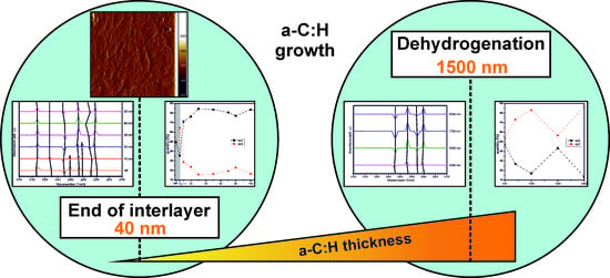
The X-ray photoelectron spectroscopy (XPS) and near-edge X-ray absorption fine structure (NEXAFS) measurements were performed at the synchrotron BESSY, Helmholtz-Zentrum Berlin, during the low-alpha phase and used as supportive studies of the carbon bond state on the surface. The used HE-SGM beamline system is described elsewhere [33]. To prevent charge-induced effects on the sample surface it is additionally equipped with a flood gun.
During the XPS measurements, a full spectrum (700 to 0 eV) was first recorded. This survey provides an overview of the entire chemical surface composition. The C1s peak was examined to analyze the different binding states of the carbon atoms. These measurements were performed at least at two different sample sites to check reproducibility, homogeneity, and the stability of the deposited a-C:H layers. For the analysis of the received spectra and the deconvolution of the C1s spectra, the commercially available software CasaXPS (software version 2.3.18, Casa Software Ltd., Teignmouth, UK) was used. The percentages of sp2, sp3, C–O, and C=O bonds in the total C1s peak were identified, where C–O bonds were evaluated as sp3 bond and the C=O bond as sp2-bonded carbon, and related to the corresponding thicknesses. To compensate for static charges, the scale of the binding energy was corrected in the evaluations. The C1s peak was set to a value of 284.8 eV [33].
The C as well as the O K-edges were recorded with NEXAFS. For the C K edge, measurements were taken on at least two different surface sites to ensure accuracy. O K-edges were recorded to check the presence or absence of oxygen. All measurements were performed in partial electron yield (PEY) in which a counter voltage is applied. In this way, the measurement electronics are not reached by all the electrons leaving the material, meaning it is very surface sensitive [34]. Detector and sample geometry followed an incidence angle of 55°. The C K-edges were analyzed using Origin 8.1 commercial software. For the analysis according to Watts et al. [35], it was necessary to first normalize the spectra and then adjust them to the decreasing ring current present at the BESSY experimental station. Subsequently, a correction with a previously measured gold edge was performed to eliminate a possible contamination of the grid. Further analysis was performed using a self-written peak evaluation program combined with Origin 8.1 software.

3. Results

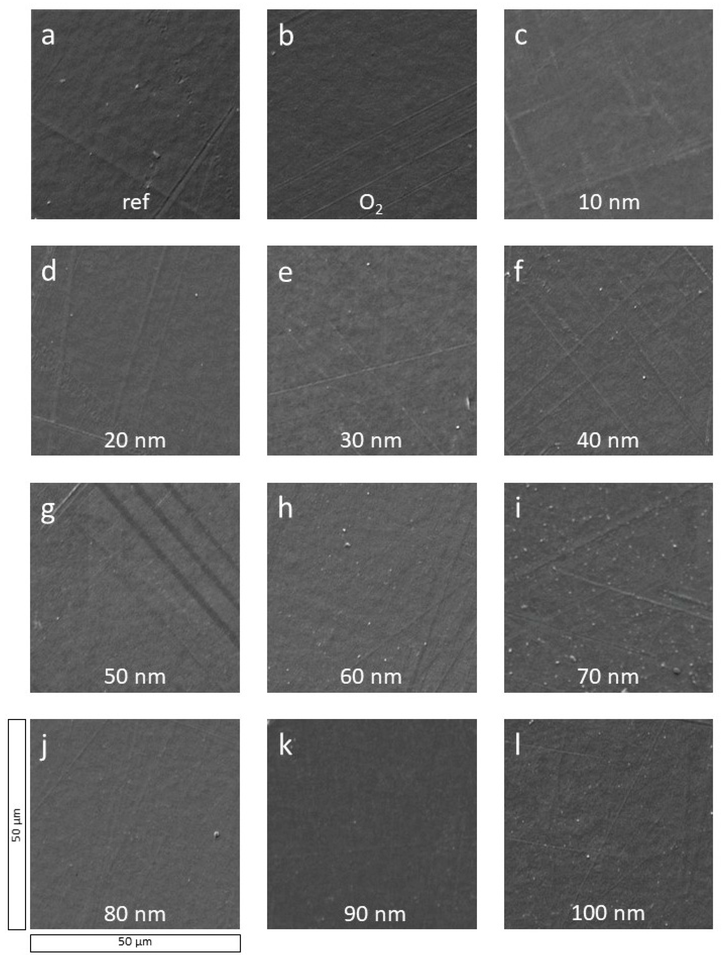
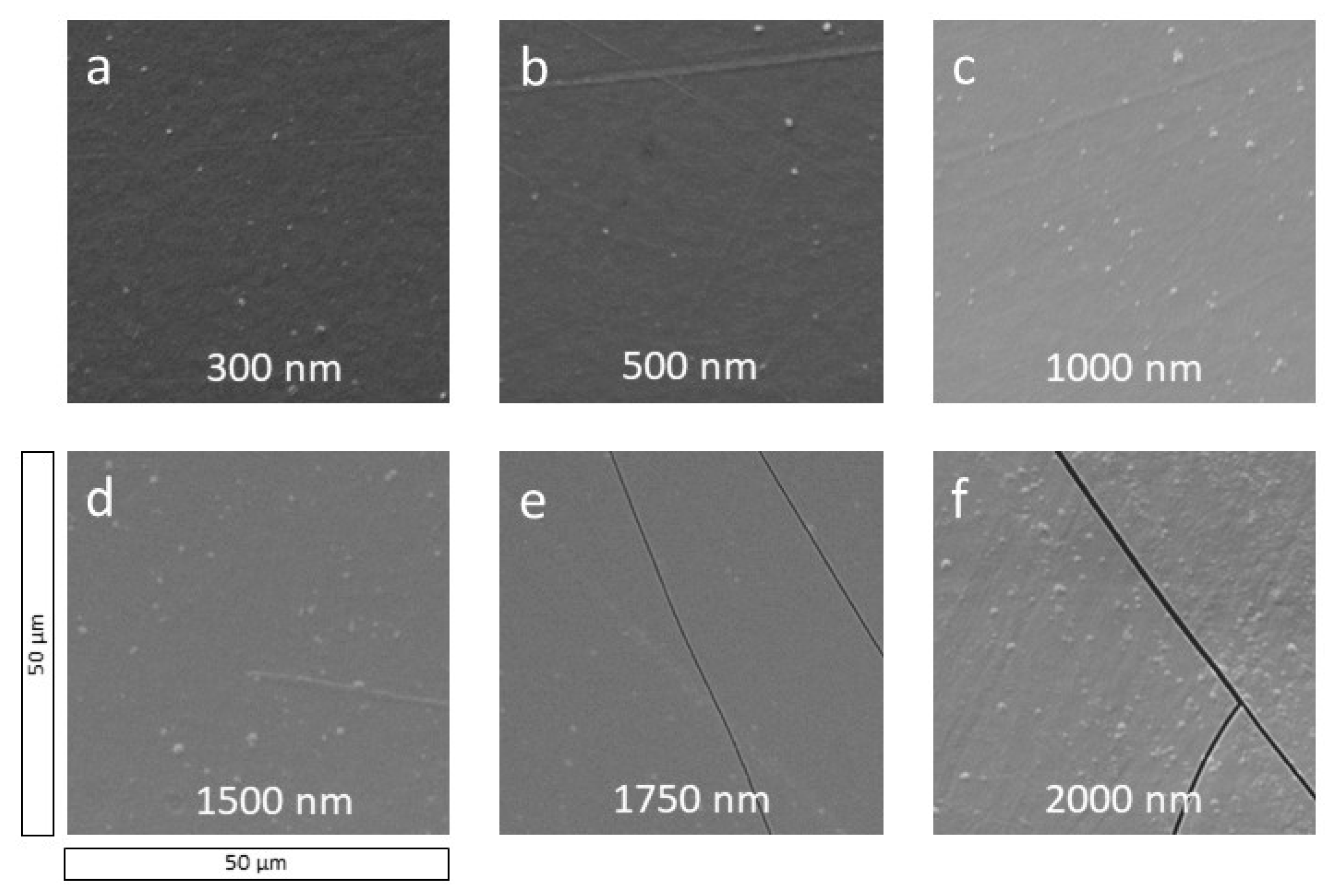
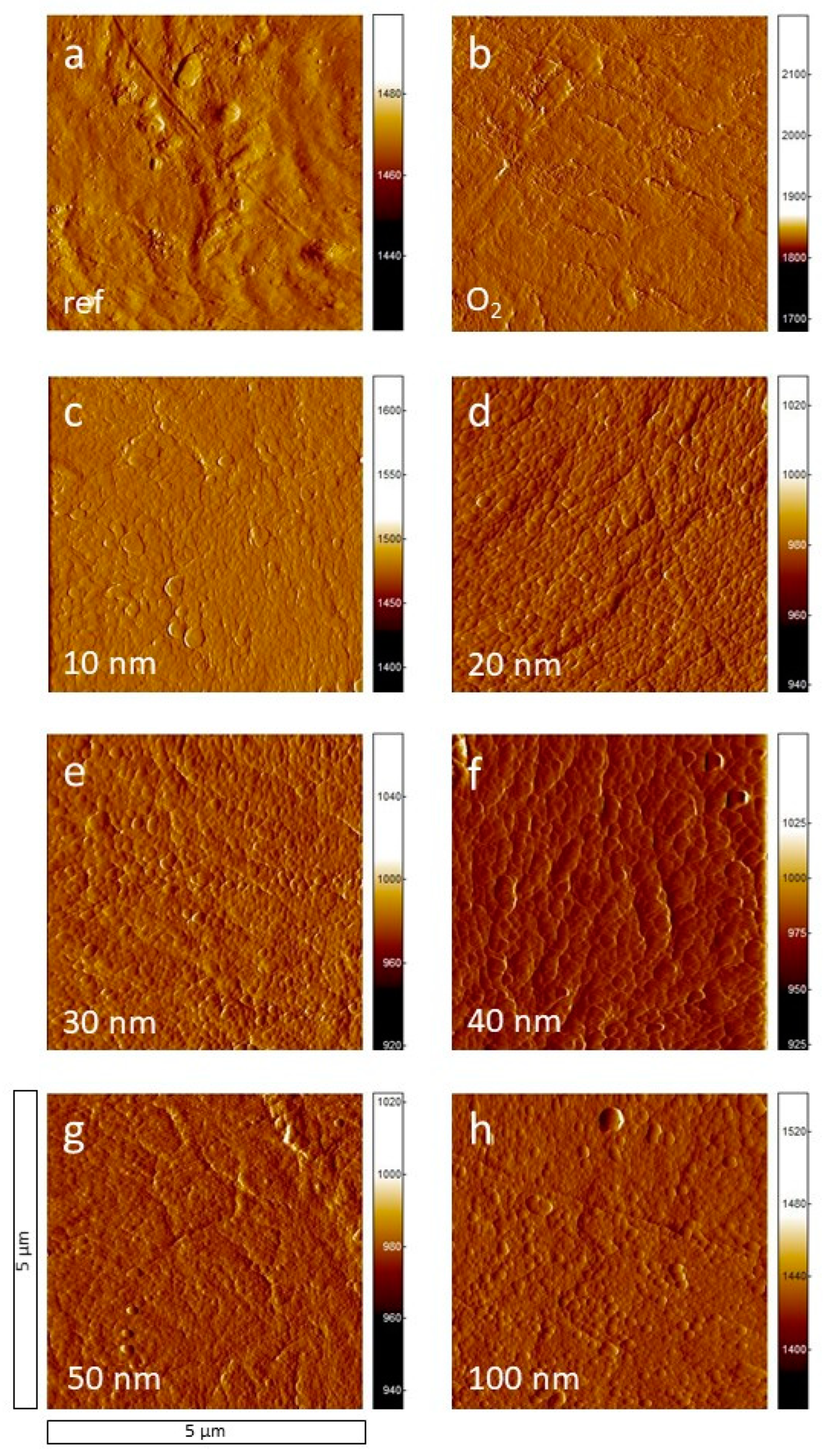
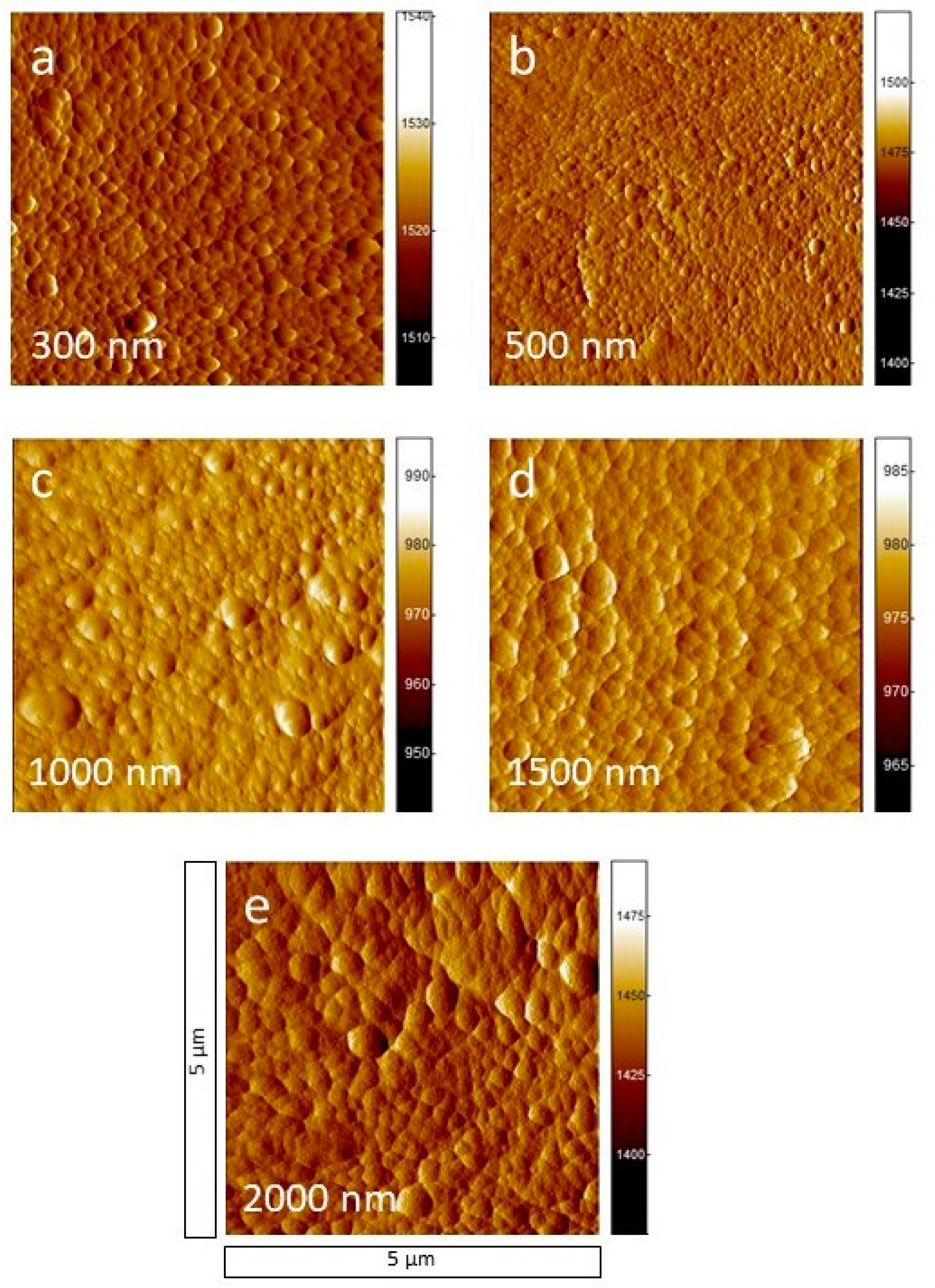
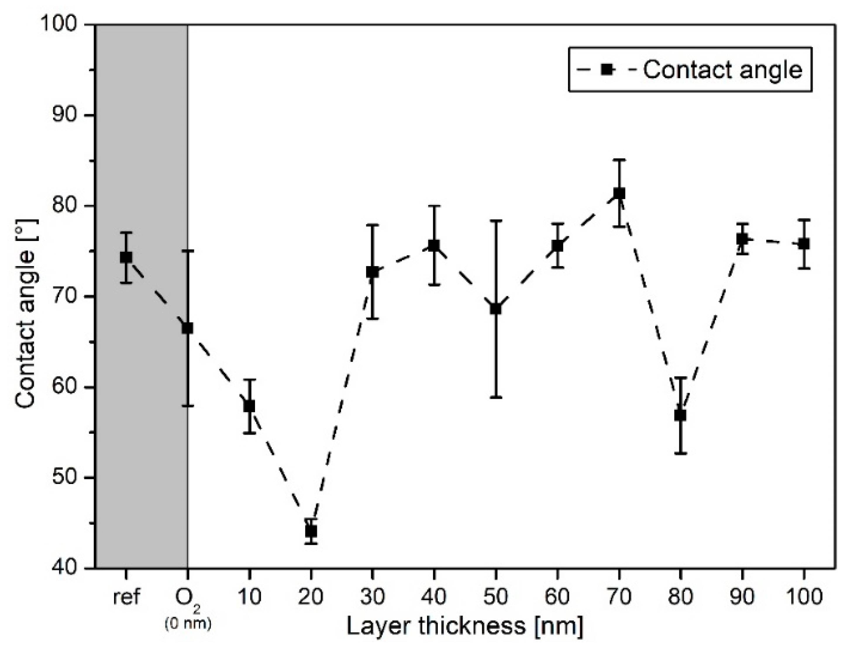
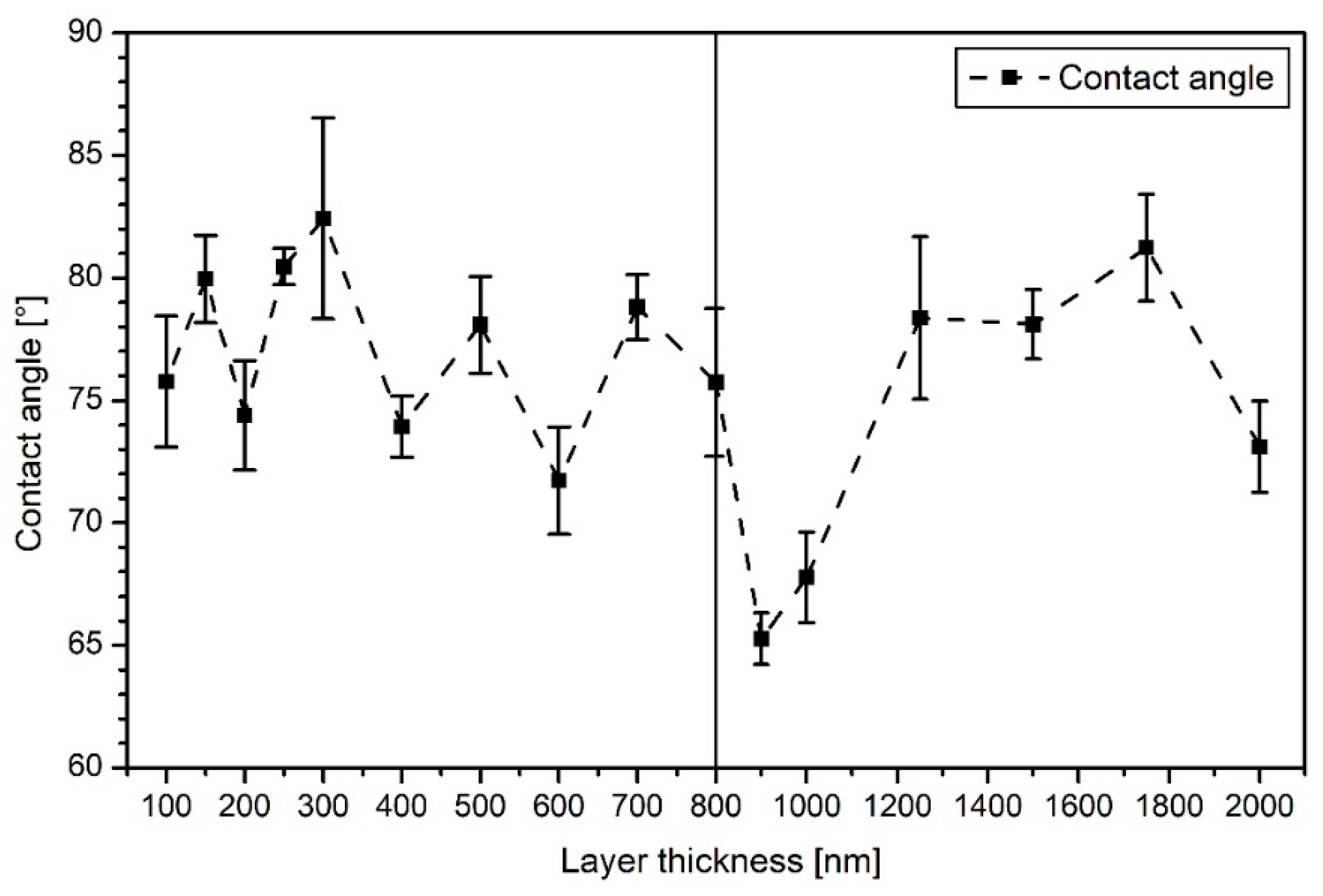
3.1. Surface Morphology

First, SEM images are discussed to get an overview of the layer condition. Figure 1 shows the reference sample (Figure 1a), the O2 plasma-treated sample (Figure 1b), and a-C:H coated samples up to a layer thickness of 100 nm (Figure 1c–l). Thicker layers are displayed in Figure 2.
The reference sample of PA6 (Figure 1a) is strongly structured and shows many scratches, which are due to the production process. Additionally, some minor impurities in the form of particles are visible. The O2 plasma-treated sample (Figure 1b) is smoother and has fewer scratches. In addition, there are less dirt particles on the surface. With the application of a-C:H layers of increasing thickness starting at 10 nm (Figure 1c–l) the scratches become weaker as they are covered with the a-C:H layer. The deposited layer is closed and appears homogeneous. On the 50 nm sample (Figure 1g) three black stripes are visible. Here, the gold layer applied for the SEM measurements is probably damaged, which leads to charging effects and thus to a darker appearance. With increasing thickness, the scratches of the base material are still visible, but the layer appears closed overall and adheres well.
In Figure 2a–f, the up to 2 µm thick a-C:H layers deposited on PA6 are shown. With 300 nm (Figure 2a) the surface of the layer is homogeneous and closed. The scratches are further attenuated. This behavior continues up to 1500 nm (Figure 2b–d), but when the a-C:H layer reaches 1750 nm (Figure 2e), the layer breaks up. The layer failure continues with the PA6 sample coated with 2000 nm (Figure 2f).
For a detailed investigation of the surface morphology, high-resolution AFM measurements were performed. Figure 3a shows the surface morphology of raw PA6 (reference sample), the PA6 cleaned with oxygen plasma (Figure 3b), and PA6 covered with a-C:H layers from 10 to 100 nm (Figure 3c–h) in ascending order. The measured area has a size of 5 µm × 5 µm, the roughness values for the AFM measurements (raw PA6 to 2000 nm a-C:H@PA6) are shown in Table 1. The roughness Rq is in the interval of 5.12 ± 0.55 nm (1000 nm deposition) and 9.20 ± 0.11 nm (100 nm deposition) for all samples measured resulting in a relatively smooth layer. For the raw and the O2 plasma-treated PA6 sample, the surface is bumpy and shows some scratches, which could be a result of the manufacturing process. Some particles which are visible on the AFM image can be dust or dirt. These are unavoidable due to the industrial production of the samples and the prevalent environment there. For the AFM images, the surface of the oxygen-treated sample (Figure 3b) appears to be a little more roughened compared to the raw material (Rq of 6.81 ± 1.10 nm compared to 6.21 ± 0.68 nm), which is most likely caused by the oxygen bombardment. Additionally, some scratches are still visible. With the deposition of a 10 nm a-C:H layer on PA6 (Figure 3c), the surface is covered by small, unstructured, grain-like particles resulting in a raised Rq value of 8.22 ± 1.31 nm. This more uneven morphology of the coating decreases with increasing a-C:H layer thickness and an overall more even layer is formed, which has a defined grain-like morphology. This starts with a thickness of 40 nm. The beginning growth of a homogeneous grain structure resp. layer represents the completion of the interlayer phase [14]. Here, the roughness is 9.04 ± 0.92 nm and nearly at its maximum value. The interlayer is a mixed phase of polymer and a-C:H layer, whose thickness can be estimated to 40 nm by the current AFM investigations. The start of the normal layer growth at 50 nm a-C:H thickness is accompanied by a lower Rq (8.73 ± 0.58 nm). The scratches already visible on raw PA6 are still visible on thinner layers, especially on a-C:H layers of 20, 30, and 100 nm (Figure 3d,e,h). This behavior is similar to that of such a-C:H layers on high-density polyethylene (HDPE), which have already been investigated by Catena et al. [14].
Figure 4 shows the AFM images of the deposition of thicker a-C:H layers from 300 up to 2000 nm. The homogeneous grain structure, which became observable for the thin layers beginning at 40 nm, continues for the 300 nm layer (Figure 4a). With a thickness of 500 nm (Figure 4b) the majority of the grains becomes smaller compared to the grains of the 300 nm layer (Rq of 6.14 ± 0.91 nm compared to 6.74 ± 0.27 nm). This may be a consequence of a new grain layer starting on top of the previous closed one at a lower thickness. The AFM images for 1000, 1500, and 2000 nm (Figure 4c–e) show smoother grains than before, resulting in the lowest surface roughness of 5.12 ± 0.55 nm at 2000 nm a-C:H layer thickness. They become more regularly spaced, but differences in grain size remain constant. The AFM images confirm the homogeneous surface coating of the PA6 samples with a-C:H for higher layer thicknesses, as already indicated by the SEM (Figure 2). For thin layers, it could also be determined that this homogeneous layer growth starts only at about 40 nm with the completion of the interlayer. This could not be detected on the SEM due to its lower resolution. However, with SEM it was possible to show the layer failure at higher layer thicknesses which, of course, is poorly detectable in AFM. Here, both techniques complement each other well.
CA measurements were performed for further analysis of the surface characteristics. The wettability of the surface and thus the resulting CAs of the investigated a-C:H layers are influenced by three factors: (I) the morphology of the surface [36,37,38]; (II) the different carbon hybridization states on the surface [18,21,39,40,41]; and (III) the existing chemical bonds [42,43,44,45]. A detailed description is summarized in a previous paper by some of the authors [26].
For a better overview, the CA evaluation is divided into two diagrams. Figure 5 shows the CAs obtained for the series of a-C:H layers from 10 to 100 nm deposited on PA6. Additionally, the CA of the raw and e O2 plasma-cleaned PA6 are shown. The plasma-cleaned sample is used here as the reference since all a-C:H deposited samples were previously O2 plasma cleaned. For the raw PA6 polymer the CA is 74° and within the limits of the literature values [46]. With O2 plasma treatment, the angle decreases to 66°. As discussed earlier, this is due to the presence of functional oxygen groups. The surface becomes more hydrophilic and the CA decreases. With the application of 10 nm a-C:H layer, the CA drops rapidly to 58°. This behavior continues until the 20 nm deposition, where the lowest measured value of 44° is reached for the present series. If the film thickness is increased to 30 nm, the CA changes to 72°. Up to a layer thickness of 60 nm, the CA varies between 68° and 76°, meaning it remains relatively constant within the error margins, even for the relatively large error at 50 nm. This also indicates the completion of the interlayer phase in the 30 to 40 nm region, since a new growth phase starts. With a layer thickness of 80 nm the CA decreases again sharply to 57° before returning to 75° at 90 nm. In summary, for the thin film depositions (10 to 100 nm, Figure 5) according to the CAs, an overall similar film is obtained, with few exceptions only after reaching 30 nm, despite continued growth resp. increase of layer thickness. For 30 to 100 nm a-C:H and the raw PA6, with the exception of 80 nm deposition, the CA values are comparatively high, which is associated with a sp2-like carbon hybridization. The CA of the 10, 20, and 80 nm depositions are below 60°, which indicates a more sp3-like hybridization of the carbon atoms.
The gray box depicts values for the raw polymer and the O2 plasma-pretreated sample. The layer thickness of 0 nm is depicted by the O2 sample.
Figure 6 shows the CA measurements for the thicker a-C:H depositions from 100 to 2000 nm on PA6. For the layers between 100 and 800 nm, the CAs alternate between 75° and 82°. With reaching a layer thickness of 900 nm, the CA decreases to 65°, but recovers at 1250 nm within 78° and 81° until 1750 nm. At 2000 nm, the CA decreases again. The temporarily strong decrease in CAs between 800 and 1250 nm may indicate a change of the hybridization state to a more sp3-dominated network. It is also conceivable that dehydrogenation of the layer occurs right after, resulting in a higher contact angle due to the higher amount of sp2-bound carbon, i.e., a reduced proportion of hydrogen in the bonds present. This has already been proven for HDPE in this a-C:H thickness range [14,23]. The error of the CA measurements is relatively small in most cases, which suggests a flat, homogeneous surface, as already visible in SEM (Figure 1 and Figure 2) and AFM (Figure 3 and Figure 4). For the layers above 1750 nm, which were visibly broken in SEM (Figure 2e,f), a larger error was to be expected due to the non-closed surface. The relatively small error is possibly due to the limited amount of cracks. A change in the bonding ratio of the carbon atoms and the CAs, as in other materials before, could not be observed [24,25].

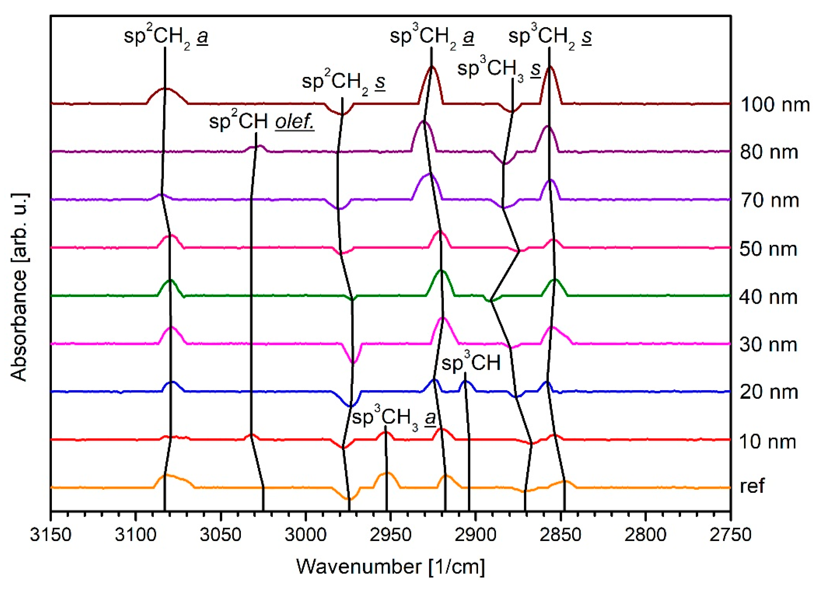
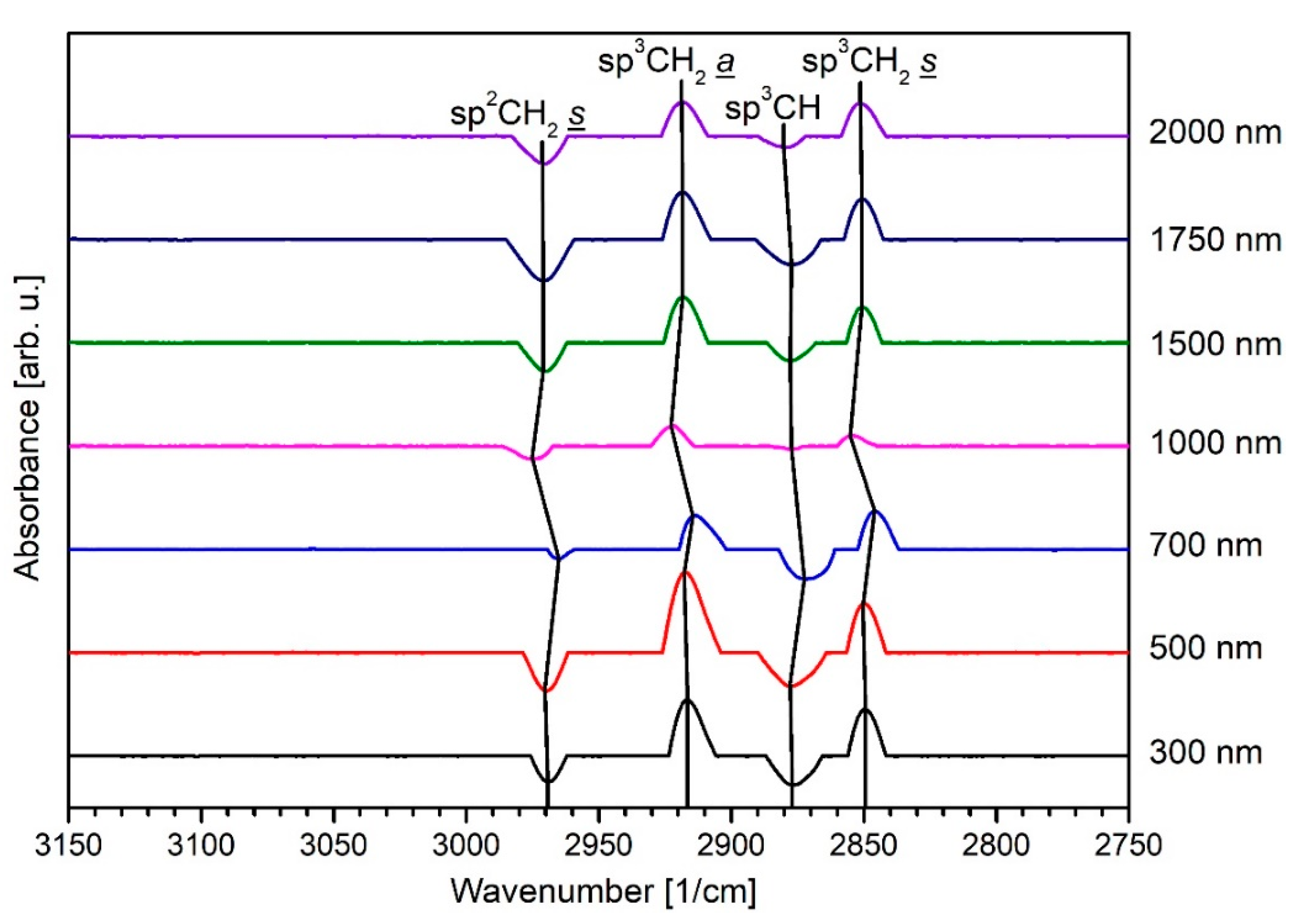
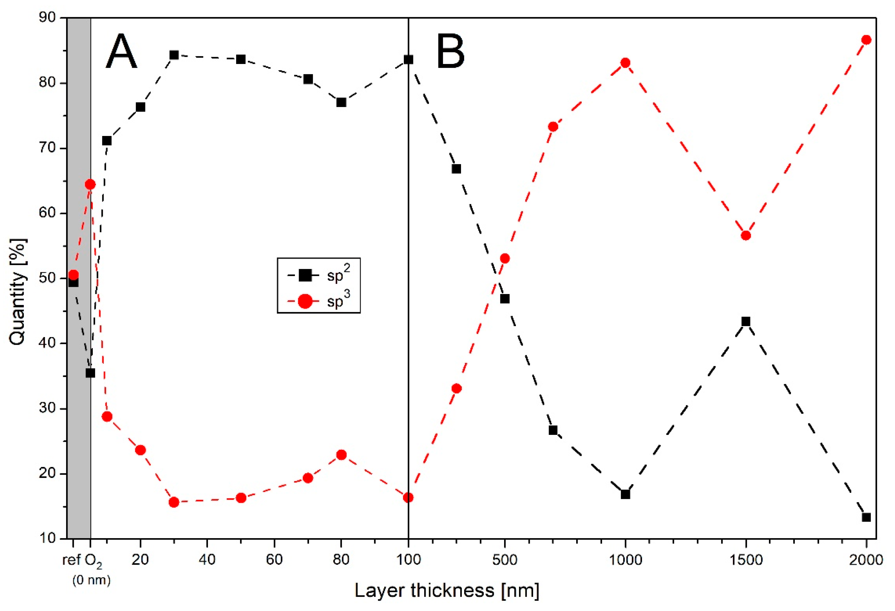
3.2. Infrared Spectroscopy

DRIFT spectroscopy allows examining differences in the chemical composition of the a-C:H layers deposited on the PA6 samples as a function of their specific thickness. In particular, the measurements presented here provide information on the various sp2 and sp3 bonds of the carbon atoms present in the layers. The results of the DRIFT spectra in Figure 7 and Figure 8 are evaluated on the basis of own results and those of other groups [15,16,47,48]. The O2 plasma-treated PA6 is used as a reference (“background”) for the samples investigated here since all a-C:H layers are deposited on a previously oxygen-treated PA6 surface.
Figure 7 and Figure 8 show the corresponding spectra in ascending order plotted in arbitrary units (arb. u.). For a better overview, the obtained results are shown separately: the raw PA6 sample and the thinner a-C:H layers from 10 to 100 nm are plotted in Figure 7, the thicker layers from 300 to 2000 nm in Figure 8. Thinner layers were coated and measured in 10 nm steps due to special interest in the interlayer formation taking place in this region. Figure 7 shows that a total of eight different oscillations of carbon bonds occur for the thin layers. It is noticeable that the peak orientation according to the PA6 sample treated with O2 plasma contains more sp3 (sp3CH3 a = asymmetric at 2952 cm−1, sp3CH2 a is at 2917 cm−1, and sp3CH2 s = symmetric at 2847 cm−1 [47,48]) to both the raw polymer and all a-C:H layers. The lower proportion of sp3 bonds on the surface of the raw polymer is due to impurities that have settled there and been removed by the oxygen plasma. In addition, only two of the bonds measured are absorption oscillations: the comparatively dominant sp2CH2 s oscillation at 2974 cm−1 and the sp3CH3 s at 2871 cm−1 [48], which is relatively weak. For the layers, this means that the carbon is mostly sp2 bounded. Vibrations for sp2CH olefinic (3032 cm−1 [48]) are only visible for the 10 and 80 nm a-C:H layer, and they are comparatively weak and will not be further discussed.
The sp3CH3 a peak is also not discussed further, as it is only available for the reference sample and the 10 nm a-C:H coating. Since this layer thickness corresponds approximately to the measuring depth, signals of the PA6 material are transmitted. In the course of the current coating process, the surface of the a-C:H layer undergoes some chemical changes, which are characterized by peaks of varying intensity. Overall, however, the same bond oscillations are observed for all measured layer thicknesses. A noticeable change as function of film thickness is a significant shift in the peaks, i.e., a slight change of the peak positions. A shift to a larger wave number means, here, a higher C–H binding energy. This is expressed by a smaller binding distance between the C–H atoms [32]. The sp2CH2 a bond shifts to a higher wavenumber at a layer thickness of 80 nm. The sp2CH2 s bond, in contrast, undergoes several shifts. Firstly, during layer growth to 10 nm to higher wavenumbers, and then returning to the old position when changing to 20 nm. After reaching a layer thickness of 40 nm, the peak shifts again to higher wavenumbers. The sp3 bonds carry out a large number of shifts and change minimally at almost any layer thickness. Changing binding distances, recognizable by frequencies shifting back, indicate a changing in chemical composition. Thus, a chemically very variable environment is present on the surface with sp2-dominated absorption behavior. A large number of well-formed sp3 peaks, which are not absorption peaks, indicate a lower sp3 content compared to the O2 plasma-treated sample and support the statement of sp2 dominated growth for the first 100 nm layer thickness. A similar behavior has been observed for such a-C:H coatings on other polymers [15,16,23,24,25,26].
Figure 8 shows the DRIFT measurements for the thick layers greater than 100 up to 2000 nm layer thickness. For thicker a-C:H layers on PA6, most of the peaks previously visible for thin layers disappear (compare Figure 7). A total of four oscillations of carbon bonds can be identified. As absorption peaks, the sp2CH2 s and the sp3CH peak as well as the oscillations of the symmetric and asymmetric sp3CH2 bond are also visible. These indicate their presence in the O2-treated sample, but not or only to a relatively small extent in the a-C:H layers. As with the thin layers, all bonds undergo a large number of position shifts, so the surface is chemically very variable. For 300 and 500 nm, the peaks for the sp2 and sp3 oscillation are both well defined. With a change to 700 nm film thickness, the sp3CH bond dominates the absorption peaks. This indicates that with increasing a-C:H layer thickness, more sp3 bonds are formed. These bindings are very strong in comparison to sp2 and sp bonds, due to their tetrahedral shape [21]. When the 1500 nm thickness is reached, the sp3 bond weakens and the sp2 bond becomes dominant until 2000 nm. Additionally, with reaching the 1500 nm a-C:H, all peaks shift back to their values from the beginning. This is an indication of the dehydrogenation of the layer. Hydrogen is released from the carbon sp3 bonds by conversion to sp2 bonds, whose proportion increases. This is in line with the results of the CA measurements which is rising in this film thickness region. Dehydrogenation could already be observed for HDPE for a similar thickness range [14,23].

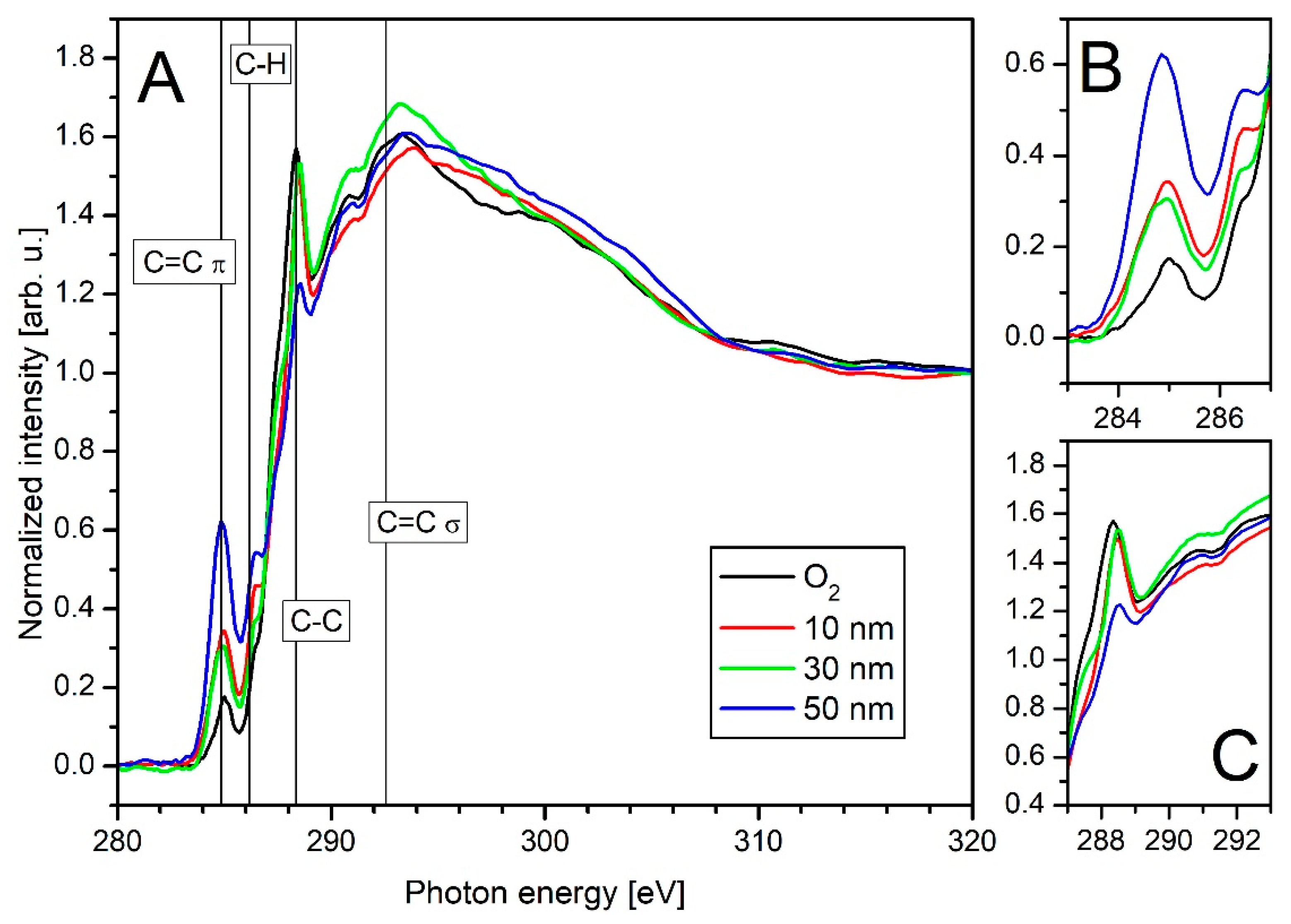
3.3. X-ray Spectroscopy

For further analysis of the chemical composition of the deposited a-C:H layers on PA6, measurements were performed using the X-ray synchrotron-based techniques XPS and NEXAFS. Figure 9 shows the evaluated results for the XPS measurements (for deconvolution results, see Supplementary Material). Here, the sp2 and sp3 bonds are plotted as a function of film thickness. Peak positions were identified using the NIST database and other publications [24,25,49,50,51]. For a better overview, the graph has been separated into Figure 9A for thin films from 0 to 100 nm (including the raw PA6 and O2 plasma-treated sample) and Figure 9B for thick films from 100 to 2000 nm. A more detailed analysis of the thinner layers was carried out to investigate the formation of the interlayer, which is a mixture of base polymer and the a-C:H layer.
The existence of the interlayer has already been proven for other polymers such as polyethylene terephthalate (PET) and HDPE [14,15,23,28], and in the case of HDPE its thickness has also been determined by X-ray spectroscopic analysis methods and DRIFT measurements [23]. For the raw polymer, about 50% sp2- and 50% sp3-bound carbon were determined (Figure 9A). Considering the structure of the raw polymer, an almost pure sp3 structure is expected and the raw polymer is obviously dirty. This may be from residues resp. contaminants of the manufacturing process or softeners detaching from the polymer over time. The contamination was already detectable in the DRIFT measurements, where pronounced sp2 oscillations are visible (Figure 7). With the O2 plasma treatment, the amount of sp2 bonds present was strongly reduced and the surface was cleaned and activated. For this reason, all samples coated later on were first O2 plasma treated. With the application of a 10 nm thick a-C:H layer, the proportion of sp2 bonds increases again at the cost of decreasing sp3 bonds. This trend continues with increasing layer thickness until a thickness of 30 nm is reached. Here, the sp3 bonds have the lowest proportion and the layer composition remains almost constant up to 50 nm. The increased sp3 content up to 30 nm is probably due to fragments of the base polymer, which are deposited in the interlayer phase with layer components. With increasing layer thickness, their percentage in the interlayer decreases, since the base material is no longer available due to possible erosion processes. The interlayer phase ends with a layer thickness of about 30 nm and pure a-C:H growth begins. After reaching 50 nm film thickness, the sp3 content increases again but reaches only 23% at 80 nm. At 100 nm, this value is again 17%. From the completion of the interlayer to 100 nm layer thickness, the value of sp2- and sp3-bound carbon is almost constant, even if there are small fluctuations. The dominance of sp2 bonds and decreasing proportion of sp3 bonds, which are visible in XPS, were already seen in the DRIFT measurements. The CA measurements also indicate a strong sp2 dominance for thin films, and the increase in sp3 bonds at 80 nm is also visible there. Therefore, all techniques reveal a very similar behavior.
Figure 9B shows the thicker layers from 100 to 2000 nm. If the layer thickness increases, the bonding ratio at the surface of the a-C:H layer starts to change. The proportion of sp3 bonds increases strongly, and at 500 nm the bond ratio changes to sp3-dominated a-C:H growth. At 1000 nm, about 83% of the carbon is sp3 bound at the surface. With the step to 1500 nm, the proportion of sp2 bonds increases strongly again to 43%. This is due to the dehydrogenation of the layer. Hydrogen leaves the layer at the expense of the sp3 bonds. This leads to a re-hybridization of the carbon atom orbitals. The now free bonds of the previously sp3-bound carbon changes into sp2-hybridized carbon clusters. The decrease in sp3 bonds in favor of increasing sp2 bonds was already visible in the DRIFT (Figure 8) starting at 1500 nm. Moreover, the coalescence phenomenon of the fusion of grains on the surface takes place in this region, as demonstrated by some authors [14]. This behavior has already been demonstrated for HDPE [14,23]. If the thickness of the layer increases again, the effect decreases, and carbon is again strongly sp3 bound at 2000 nm. The XPS results clearly show that layer growth up to 100 nm is sp2 dominated and towards thicker layers a more rigid, sp3-dominated carbon network is present on the surface. Exceptions are the interlayer region, which is limited to the first 30 nm layer thickness and the zone of dehydrogenation at 1500 nm a-C:H layer.
For thin layers, additional NEXAFS measurements have been performed. The spectra of the O2 plasma-treated PA6 together with various thin a-C:H layers on PA6 (10, 30, and 50 nm) are shown in Figure 10. The recording and evaluation of the raw data are performed as described earlier in the Section 2.4 experimental section (2.4). In consideration of the work of other groups, the peak positions were determined as follows: C=C π (284.85 eV), C–H (286.15 eV), C–C (288.35 eV), and C=C σ (292.55 eV) [52,53,54,55,56]. For a better overview, the figure is divided in three areas: A for the full spectra of the carbon C K-edge from 280–320 eV, B for the area of 293–287 eV for the C=C π, and C from 287–293 eV for the C–C binding.
For the O2 plasma-treated sample (black curve) it is noticeable that the C=C π peak belonging to the sp2 is only very weakly pronounced at 284.85 eV, while the C–C peak, which represents the sp3 bonds, is strongly emphasized. This corresponds to the previous DRIFT and XPS results. With the application of a 10 nm a-C:H layer (red curve), the sp2 fraction increases, but the sp3 fraction remains almost unchanged. In addition to the sp3 bonds (C–C peak) of the substrate, there are also sp2 bonds (C=C π peak) detectable due to the deposited layer. If the layer thickness is increased to 30 nm (green curve), a spectrum similar to that of the 10 nm sample is obtained. In both curves, the sp3 content most likely comes from the base material and is part of the interlayer. However, if the layer thickness of 50 nm is reached (blue curve), the measured spectrum changes significantly. The C=C π increases strongly while the C–C peak almost disappears. The reason for the disappearance of the C–C peak is that it was caused by the base material which was mixed with the a-C:H layer in the interlayer. At 50 nm layer thickness, only the pure a-C:H layer is measured. The end of the interlayer phase is therefore specified between 30 and 50 nm thickness, which was already shown in the AFM, CA, DRIFT, and XPS measurements.

4. Conclusions

Polymer PA6 was coated with a-C:H layers in various thicknesses (10–2000 nm) using RF-PECVD generated acetylene plasma. The a-C:H layers were analyzed in two separate ranges: thin ones up to 100 nm to investigate the interlayer phase and thick layers between 100 and 2000 nm to investigate the dehydrogenation. The SEM images show stable a-C:H layers on PA6 samples, provided that the layer thickness of 1500 nm is not exceeded. Here, dehydrogenation also takes place, leading to a decrease in sp3 bonds in favor of sp2 bonds. The layer failure can be attributed to a stress reduction due to the sp3 dominance still present in this region.
AFM, CA, DRIFT, and XPS measurements show that the interlayer formation for a-C:H films on PA6 is completed by 40 nm. In the AFM measurements, a homogeneous grain structure can be seen from here on. In the CAs, a relatively constant angle for the thin films is obtained after 40 nm. In XPS, the sp3 content, which is lifted from the raw material into the interlayer mixed phase, is almost constant and low and a pure, sp2 containing a-C:H layer grows up. This behavior changes only after the layer thickness exceeds 100 nm and the carbon in the layer begins to be more strongly sp3 bound. The SEM and AFM measurements show equally stable growth. In the further course, the sp3 content increases significantly until dehydrogenation takes place at 1500 nm and stress-induced layer failure occurs later on.
Furthermore, it can be seen that the bonding ratios of the carbon atoms depend not only on the selected plasma parameters, but also on the achieved layer thickness, which clearly underlines the changing character of the a-C:H layer with increasing thickness. Both DRIFT and XPS measurements show a change between sp3- and sp2-dominant bound layers. Since the change in bond dominance also causes a change in the properties of the applied layer, these can be controlled accordingly and adjusted by the layer thickness. The thickness and the chemical environment of the interlayer between PA6 and the a-C:H layer could also be determined, very accurately, to 40 nm. This value is therefore very pronounced and also explains the high stability of the applied a-C:H layer before it breaks up at 1750 nm. The dehydrogenation of the layer at high thicknesses, which is also known for other coated polymers, could also be proven.
In the process of the studies, it was shown that a-C:H layers can be deposited successfully on the PA6 material and remain stable (= without cracks) up to a thickness of 1500 nm. The layer also adheres properly to the polymer (interlayer = 40 nm). It is therefore possible to refine PA6 for applications such as in the (food) packaging sector (e.g., changed barrier effects).

Supplementary Materials

The following are available online at https://0-www-mdpi-com.brum.beds.ac.uk/article/10.3390/polym13111886/s1, Figure S1: XPS C1s Peak deconvolution for the reference, O2 plasma treated sample and the thin layers from 10–100 nm a-C:H film thickness, Figure S2: XPS C1s Peak deconvolution for the PA6 samples coated with thick a-C:H layers (300–2000 nm).

Author Contributions

Conceptualization of the study, developing and organization of processes was arranged by T.S. and C.B.F.; T.S. prepared the samples and performed the data acquisition and evaluation of XPS and NEXAFS, evaluation of SEM results, overall data curation, visualization and wrote the manuscript draft. H.L. contributed in terms of contact angle, AFM and DRIFT measurements, their evaluation and visualization. L.B. and M.F. contributed in the acquisition of synchrotron measurements, XPS and NEXAFS. Y.B. arranged SEM imaging of thin layers (<1000 nm) and M.B. SEM imaging of thick layers (1000–2000 nm) and were supervised by B.H., T.S. and C.B.F.; T.S. and C.B.F. validated the results, reviewed and edited the manuscript. Both S.W. and C.B.F. contributed in terms of funding acquisition, project administration, supervision and overall guidance in the study. All authors have read and agreed to the published version of the manuscript.

Funding

T.S., L.B., and C.B.F. gratefully acknowledge the financial support (funding agreement BESSY 2: 145 and 225) provided by the Helmholtz-Zentrum Berlin (HZB), Germany.

Institutional Review Board Statement

Not applicable.

Informed Consent Statement

Not applicable.

Data Availability Statement

The data presented in this study are available on request from the corresponding author.

Acknowledgments

The authors thank Heinz Busch (NTTF Coatings GmbH, Rheinbreitbach, Germany) for the possibility of industrial coating of the samples. We also thank Joachim Scholz (University of Koblenz-Landau, Department of Chemistry) for the DRIFT equipment and Alexei Nefedov from KIT (Karlsruhe Institute for Technology, Group: Chemistry of oxidic and organic interfaces; X-ray and Electron Spectroscopy at Interfaces) for beamtime support. We thank HZB for the allocation of synchrotron radiation beamtime. The authors thankfully acknowledge the financial support by the Helmholtz-Zentrum Berlin (HZB), Germany.

Conflicts of Interest

The authors declare no conflict of interest.

References

  1. Hellerich, W.; Harsch, G.; Haenle, S. Werkstoff-Führer Kunststoffe: Eigenschaften, Prüfungen, Kennwerte; mit 64 Tabellen, 7. überarb. und erw. Aufl.; Carl Hanser Verlag GmbH: München, Germany, 1996. [Google Scholar]
  2. Döring, E. Polypropylene and Polyamide Developments in the European Automotive Industry; SAE Technical Paper Series; SAE International: Warrendale, PA, USA, 1983. [Google Scholar]
  3. Nandhini, R.; Moorthy, M.K.; Muthukumaran, S.; Kumaran, S. Influence of process variables on the characteristics of friction-stir-welded polyamide 6,6 joints. Mater. Werkst. 2019, 50, 1139–1148. [Google Scholar] [CrossRef]
  4. Félix, J.S.; Monteiro, M.; Manzoli, J.E.; Padula, M.; Pezo, D.; Romero, J.; Nerín, C. Identification and migration of degradation compounds from irradiation of multilayer polyamide 6 films for meat foodstuffs and cheese. Anal. Bioanal. Chem. 2008, 391, 847–857. [Google Scholar] [CrossRef]
  5. Unal, H.; Mimaroglu, A. Friction and wear performance of polyamide 6 and graphite and wax polyamide 6 composites under dry sliding conditions. Wear 2012, 289, 132–137. [Google Scholar] [CrossRef]
  6. Karsli, N.G.; Aytac, A. Tensile and thermomechanical properties of short carbon fiber reinforced polyamide 6 composites. Compos. Part B Eng. 2013, 51, 270–275. [Google Scholar] [CrossRef]
  7. Deopura, B.L. Polyesters and Polyamides; Woodhead Publishing: Cambridge, UK; Textile Institute: Boca Raton, FL, USA, 2008. [Google Scholar]
  8. Sabbatini, L. Polymer Surface Characterization; De Gruyter: Boston, MA, USA, 2014. [Google Scholar]
  9. Andrady, A.L.; Neal, M.A. Applications and societal benefits of plastics. Philos. Trans. R. Soc. B Biol. Sci. 2009, 364, 1977–1984. [Google Scholar] [CrossRef] [PubMed]
  10. Couderc, P.; Catherine, Y. Structure and physical properties of plasma-grown amorphous hydrogenated carbon films. Thin Solid Film 1987, 146, 93–107. [Google Scholar] [CrossRef]
  11. Grill, A. Plasma-deposited diamondlike carbon and related materials. IBM J. Res. Dev. 1999, 43, 147–162. [Google Scholar] [CrossRef]
  12. Rohrbeck, M.; Fischer, C.; Wehner, S.; Meier, J.; Manz, W. DLC-coated pure bioplastic foil. Vak. Forsch. Prax. 2014, 26, 42–47. [Google Scholar] [CrossRef]
  13. Rohrbeck, M.; Körsten, S.; Fischer, C.B.; Wehner, S.; Kessler, B. Diamond-like carbon coating of a pure bioplastic foil. Thin Solid Film 2013, 545, 558–563. [Google Scholar] [CrossRef]
  14. Catena, A.; Agnello, S.; Rösken, L.M.; Bergen, H.; Recktenwald, E.; Bernsmann, F.; Busch, H.; Cannas, M.; Gelardi, F.M.; Hahn, B.; et al. Characteristics of industrially manufactured amorphous hydrogenated carbon (a-C: H) depositions on high-density polyethylene. Carbon 2016, 96, 661–671. [Google Scholar] [CrossRef]
  15. Catena, A.; Guo, Q.; Kunze, M.R.; Agnello, S.; Gelardi, F.M.; Wehner, S.; Fischer, C.B. Morphological and Chemical Evolution of Gradually Deposited Diamond-Like Carbon Films on Polyethylene Terephthalate: From Subplantation Processes to Structural Reorganization by Intrinsic Stress Release Phenomena. ACS Appl. Mater. Interfaces 2016, 8, 10636–10646. [Google Scholar] [CrossRef] [PubMed] [Green Version]
  16. Catena, A.; Kunze, M.R.; Agnello, S.; Gelardi, F.M.; Wehner, S.; Fischer, C.B. Amorphous hydrogenated carbon (a-C: H) depositions on polyoxymethylene: Substrate influence on the characteristics of the developing coatings. Surf. Coat. Technol. 2016, 307, 658–665. [Google Scholar] [CrossRef]
  17. Fruth, W.; Meerkamm, H.; Krumpiegl, T.; Schaufler, C.; Erkens, G.; Ruttor, M. Tribological behaviour of PVD-coated PA plastic material sliding against metal counterparts. Surf. Coat. Technol. 1999, 120–121, 470–475. [Google Scholar] [CrossRef]
  18. Paul, R.; Das, S.N.; Dalui, S.; Gayen, R.N.; Roy, R.K.; Bhar, R.; Pal, A.K.; Das, S. Synthesis of DLC films with different sp2/sp3 ratios and their hydrophobic behaviour. J. Phys. D Appl. Phys. 2008, 41, 1–7. [Google Scholar] [CrossRef]
  19. Mohagheghpour, E.; Rajabi, M.; Gholamipour, R.; Larijani, M.M.; Sheibani, S. Ion beam energy dependence of surface and structural properties of amorphous carbon films deposited by IBSD method on Ni–Cu alloy. J. Mater. Res. 2017, 32, 1258–1266. [Google Scholar] [CrossRef]
  20. Robertson, J. Plasma Deposition of Diamond-Like Carbon. Jpn. J. Appl. Phys. 2011, 50, 1–8. [Google Scholar] [CrossRef]
  21. Robertson, J. Diamond-like amorphous carbon. Mater. Sci. Eng. R Rep. 2002, 37, 129–281. [Google Scholar] [CrossRef] [Green Version]
  22. Lee, S.C.; Tai, F.C.; Wei, C.H. Correlation between sp2/sp3 ratio or hydrogen content and water contact angle in hydrogenated DLC film. Mater. Trans. 2007, 48, 2534–2538. [Google Scholar] [CrossRef] [Green Version]
  23. Schlebrowski, T.; Rouabeh, W.; Wehner, S.; Fischer, C.B. Specifying the interlayer turning point and dehydrogenation in a-C:H layers plasma deposited on high-density polyethylene with X-ray synchrotron techniques. Thin Solid Film 2019, 691, 1–6. [Google Scholar] [CrossRef]
  24. Schlebrowski, T.; Beucher, L.; Bazzi, H.; Hahn, B.; Wehner, S.; Fischer, C.B. Prediction of a-C: H layer failure on industrial relevant biopolymer polylactide acide (PLA) foils based on the sp2/sp3 ratio. Surf. Coat. Technol. 2019, 368, 79–87. [Google Scholar] [CrossRef]
  25. Schlebrowski, T.; Beucher, L.; Bazzi, H.; Hahn, B.; Wehner, S.; Fischer, C.B. Changing Contents of Carbon Hybridizations in Amorphous Hydrogenated Carbon Layers (a-C: H) on Sustainable Polyhydroxybutyrate (PHB) Exhibit a Significant Deterioration in Stability, Depending on Thickness. C 2019, 5, 52. [Google Scholar] [CrossRef] [Green Version]
  26. Schlebrowski, T.; Acharchi, H.; Hahn, B.; Wehner, S.; Fischer, C.B. 202 Refinement of Sustainable Polybutylene Adipate Terephthalate (PBAT) with Amorphous Hydrogenated Carbon Films (a-C:H) Revealing Film Instabilities Influenced by a Thickness-Dependent Change of sp2/sp3 Ratio. Materials 2020, 13, 1077. [Google Scholar] [CrossRef] [Green Version]
  27. Koidl, P.; Wild, C.; Dischler, B.; Wagner, J.; Ramsteiner, M. Plasma Deposition, Properties and Structure of Amorphous Hydrogenated Carbon Films. Mater. Sci. Forum 1990, 52, 41–70. [Google Scholar] [CrossRef]
  28. Fischer, C.B.; Rohrbeck, M.; Wehner, S.; Richter, M.; Schmeißer, D. Interlayer formation of diamond-like carbon coatings on industrial polyethylene: Thickness dependent surface characterization by SEM, AFM and NEXAFS. Appl. Surf. Sci. 2013, 271, 381–389. [Google Scholar] [CrossRef]
  29. Catena, A.; McJunkin, T.; Agnello, S.; Gelardi, F.M.; Wehner, S.; Fischer, C.B. Surface morphology and grain analysis of successively industrially grown amorphous hydrogenated carbon films (a-C:H) on silicon. Appl. Surf. Sci. 2015, 347, 657–667. [Google Scholar] [CrossRef]
  30. Armaroli, T.; Bécue, T.; Gautier, S. Diffuse Reflection Infrared Spectroscopy (Drifts). Oil Gas Sci. Technol. 2004, 59, 215–237. [Google Scholar] [CrossRef]
  31. D’Souza, L.; Devi, P.; Kamat, T.; Naik, C.G. Diffuse reflectance infrared fourier transform spectroscopic (DRIFTS) investigation of E.coli, Staphylococcus aureus and Candida albicans. Indian J. Mar. Sci. 2009, 38, 45–51. [Google Scholar]
  32. Günzler, H.; Gremlich, H.U. IR Spectroscopy: An. Introduction; Wiley-VCH: Weinheim, Germany, 2002. [Google Scholar]
  33. Fang, D.; He, F.; Xie, J.; Xue, L. Calibration of Binding Energy Positions with C1s for XPS Results. J. Wuhan Univ. Technol. Mat. Sci. Ed. 2020, 35, 711–718. [Google Scholar] [CrossRef]
  34. Nefedov, A.; Wöll, C. Advanced Applications of NEXAFS Spectroscopy for Functionalized Surfaces. In Book Surface Science Techniques; Bracco, G., Holst, B., Eds.; Springer: Berlin/Heidelberg, Germany, 2013. [Google Scholar]
  35. Watts, B.; Thomsen, L.; Dastoor, P.C. Methods in carbon K-edge NEXAFS: Experiment and Analysis. J. Chem. Phys. 2014, 140, 105–120. [Google Scholar] [CrossRef]
  36. Banerjee, D.; Mukherjee, S.; Chattopadhyay, K. Controlling the surface topology and hence the hydrophobicity of amorphous carbon thin films. Carbon 2010, 48, 1025–1031. [Google Scholar] [CrossRef]
  37. Barthlott, W.; Neinhuis, C. Purity of the sacred lotus, or escape from contamination in biological surfaces. Planta 1997, 202, 1–8. [Google Scholar] [CrossRef]
  38. Feng, L.; Li, S.; Li, Y.; Li, H.; Zhang, L.; Zhai, J.; Song, Y.; Liu, B.; Jiang, L.; Zhu, D. Super-Hydrophobic Surfaces. Adv. Mater. 2002, 14, 1857–1860. [Google Scholar] [CrossRef]
  39. Werder, T.; Walther, J.H.; Jaffe, R.L.; Halicioglu, T.; Koumoutsakos, P. On the Water-Carbon Interaction for Use in Molecular Dynamics Simulations of Graphite and Carbon Nanotubes. J. Phys. Chem. B 2003, 107, 1345–1352. [Google Scholar] [CrossRef]
  40. Zhou, Y.; Wang, B.; Song, X.; Li, E.; Li, G.; Zhao, S.; Yan, H. Control over the wettability of amorphous carbon films in a large range from hydrophilicity to super-hydrophobicity. Appl. Surf. Sci. 2006, 253, 2690–2694. [Google Scholar] [CrossRef]
  41. Bismarck, A.; Brostow, W.; Chiu, R.; Lobland, H.E.H.; Ho, K.K. Effects of surface plasma treatment on tribology of thermoplastic polymers. Polym. Eng. Sci. 2008, 48, 1971–1976. [Google Scholar] [CrossRef]
  42. Ostrovskaya, L.; Perevertailo, V.; Ralchenko, V.; Dementjev, A.; Loginova, O. Wettability and surface energy of oxidized and hydrogen plasma-treated diamond films. Diam. Relat. Mater. 2002, 11, 845–850. [Google Scholar] [CrossRef]
  43. Ostrovskaya, L. Studies of diamond and diamond-like film surfaces using XAES, AFM and wetting. Vacuum 2002, 68, 219–238. [Google Scholar] [CrossRef]
  44. Piazza, F.; Morell, G. Wettability of hydrogenated tetrahedral amorphous carbon. Diam. Relat. Mater. 2009, 18, 43–50. [Google Scholar] [CrossRef]
  45. Tay, B.K.; Sheeja, D.; Lau, S.P.; Guo, J. Study of surface energy of tetrahedral amorphous carbon films modified in various gas plasma. Diam. Relat. Mater. 2003, 12, 2072–2076. [Google Scholar] [CrossRef]
  46. Extrand, C.W. Water contact angles and hysteresis of polyamide surfaces. J. Colloid Interface Sci. 2002, 248, 136–142. [Google Scholar] [CrossRef]
  47. Tomasella, E.; Thomas, L.; Dubois, M.; Meunier, C. Structural and mechanical properties of a-C. Diam. Relat. Mater. 2004, 13, 1618–1624. [Google Scholar] [CrossRef]
  48. Veres, M.; Koos, M.; Pócsik, I. IR study of the formation process of polymeric hydrogenated amorphous carbon film. Diam. Relat. Mater. 2002, 11, 1110–1114. [Google Scholar] [CrossRef]
  49. Dietrich, P.M.; Horlacher, T.; Girard-Lauriault, P.L.; Gross, T.; Lippitz, A.; Min, H.; Wirth, T.; Castelli, R.; Seeberger, P.H.; Unger, W.E.S. Adlayers of Dimannoside Thiols on Gold: Surface Chemical Analysis. Langmuir 2011, 27, 4808–4815. [Google Scholar] [CrossRef] [PubMed]
  50. Solomon, J.; Madix, R.; Stöhr, J. Orientation and absolute coverage of benzene, aniline, and phenol on Ag (110) determined by NEXAFS and XPS. Surf. Sci. 1991, 255, 12–30. [Google Scholar] [CrossRef]
  51. Tai, F.C.; Lee, S.C.; Wei, C.H.; Tyan, S.L. Correlation between ID/IG Ratio from Visible Raman Spectra and sp2/sp3 Ratio from XPS Spectra of Annealed Hydrogenated DLC Film. Mater. Trans. 2006, 47, 1847–1852. [Google Scholar] [CrossRef] [Green Version]
  52. Dhez, O.; Ade, H.; Urquhart, S.; Urquhart, S. Calibrated NEXAFS spectra of some common polymers. J. Electron. Spectrosc. Relat. Phenom. 2003, 128, 85–96. [Google Scholar] [CrossRef]
  53. Diaz, J.; Monteiro, O.R.; Hussain, Z. Structure of amorphous carbon from near-edge and extended x-ray absorption spectroscopy. Phys. Rev. B 2007, 76, 094201. [Google Scholar] [CrossRef]
  54. Díaz, J.; Anders, S.; Zhou, X.; Moler, E.J.; Kellar, S.A.; Hussain, Z. Analysis of the π* and σ* bands of the x-ray absorption spectrum of amorphous carbon. Phys. Rev. B 2001, 64, 125204. [Google Scholar] [CrossRef]
  55. Stöhr, J. NEXAFS Spectroscopy; Springer: Berlin/Heidelberg, Germany, 1992. [Google Scholar]
  56. Brüster, B.; Amozoqueño, C.; Grysan, P.; Peral, I.; Watts, B.; Raquez, J.-M.; Dubois, P.; Addiego, F. Resolving Inclusion Structure and Deformation Mechanisms in Polylactide Plasticized by Reactive Extrusion. Macromol. Mater. Eng. 2017, 302, 1700326. [Google Scholar] [CrossRef]
Figure 1. SEM surface images of PA6 samples coated with thin a-C:H layers from 10 to 100 nm in 10 nm steps (cl). Additionally, the reference (a) and the O2 plasma-treated PA6 sample (b) are added.
Polymers 13 01886 g001
Figure 2. SEM analysis of thick a-C:H layers on PA6 (af). Thickness varies from (a) 300 to (f) 2000 nm, arranged in increasing layer thickness.
Polymers 13 01886 g002
Figure 3. AFM images of the raw PA6 (a), the O2 plasma-treated PA6 (b) samples, and PA6 samples coated with thin a-C:H layers of various thickness (10 to 100 nm, ch). The image size is 5 μm × 5 μm.
Polymers 13 01886 g003
Figure 4. AFM measurements for PA6 samples (ae) coated with thick a-C:H layers from (a) 300 up to (e) 2000 nm. The image size is 5 μm × 5 μm.
Polymers 13 01886 g004
Figure 5. Contact angle measurements for the PA6 samples: shown are raw and O2 plasma-treated PA6 as well as thin a-C:H layers up to 100 nm (the dashed line only indicates the trend).
Polymers 13 01886 g005
Figure 6. Contact angles of amorphous hydrogenated carbon (a-C:H) coatings of layer thicknesses from 100 to 2000 nm on PA6 samples (the dashed line only indicates a trend).
Polymers 13 01886 g006
Figure 7. DRIFT spectra of the analyzed PA6 samples coated with thin a-C:H up to 100 nm in 10 nm steps starting from the O2 plasma-treated reference. The measurement series is applied from below to above with increasing layer thickness.
Polymers 13 01886 g007
Figure 8. DRIFT spectra for PA6 samples coated with thick a-C:H from 300 to 2000 nm with increasing layer thickness from below.
Polymers 13 01886 g008
Figure 9. XPS measurements for PA6 coated with a-C:H layers of various thickness. The content of the sp2 (black squares) and sp3 (red circles) bound carbon are plotted against layer thickness: (A) thin layers from raw PA6 (ref) and O2-cleaned material (represents a layer thickness of 0 nm) to 100 nm and (B) thicker layers up to 2000 nm (the dashed line only indicates a trend). The gray box indicates the region before a-C:H coating (0 nm layer thickness).
Polymers 13 01886 g009
Figure 10. C K-edge NEXAFS measurements for PA6 coated with thin layers of a-C:H: (A) shows the full spectra; (B,C) present detailed photon energy intervals for carbon relevant peaks. (B): 283.00 to 287.00 eV for the C=C π peak (284.85 eV) and the C–H peak (286.15 eV); (C): 287.00 to 293.00 eV for the C–C and C=C σ (288.15 eV and 292.58 eV).
Polymers 13 01886 g010
Table 1. AFM roughness values Ra and Rq for the reference, the O2 plasma-treated, and with PA6 samples coated with thin a-C:H layers of various thickness.
SampleRa [nm]Rq [nm]
Reference4.74 ± 0.376.21 ± 0.68
O25.25 ± 0.766.81 ± 1.10
10 nm6.25 ± 1.058.22 ± 1.31
20 nm6.52 ± 0.258.25 ± 0.40
30 nm5.98 ± 0.047.61 ± 0.27
40 nm6.86 ± 0.499.04 ± 0.92
50 nm6.53 ± 0.448.73 ± 0.58
100 nm6.73 ± 0.029.20 ± 0.11
300 nm5.15 ± 0.116.74 ± 0.27
500 nm4.81 ± 0.626.14 ± 0.91
1000 nm4.86 ± 0.126.28 ± 0.18
1500 nm5.09 ± 1.906.63 ± 2.12
2000 nm3.98 ± 0.295.12 ± 0.55
Publisher’s Note: MDPI stays neutral with regard to jurisdictional claims in published maps and institutional affiliations.

