
Assessment of Pre-Treatment Techniques for Coarse Printed Circuit Boards (PCBs) Recycling


1
Discipline of Chemical Engineering, School of Engineering, Monash University Malaysia, Subang Jaya 47500, Malaysia
2
Department of Earth Resources Engineering, University of Moratuwa, Moratuwa 10400, Sri Lanka
*
Author to whom correspondence should be addressed.
Minerals 2021, 11(10), 1134; https://0-doi-org.brum.beds.ac.uk/10.3390/min11101134
Submission received: 25 September 2021
/
Revised: 11 October 2021
/
Accepted: 12 October 2021
/
Published: 15 October 2021
(This article belongs to the Special Issue Current Status of Electronic Waste Management and Value Recovery Operations—a Step towards the United Nations Sustainable Development Goals (SDGs))
Abstract
:Waste electrical and electronic equipment or e-waste generation has been skyrocketing over the last decades. This poses waste management and value recovery challenges, especially in developing countries. Printed circuit boards (PCBs) are mainly employed in value recovery operations. Despite the high energy costs of generating crushed and milled particles of the order of several microns, those are employed in conventional hydrometallurgical techniques. Coarse PCB pieces (of order a few centimetres) based value recovery operations are not reported at the industrial scale as the complexities of the internal structure of PCBs limit efficient metal and non-metal separation. Since coarse PCB particles’ pre-treatment is of paramount importance to enhance metal and non-metal separations, thermal, mechanical, chemical and electrical pre-treatment techniques were extensively studied. It is quite evident that a single pre-treatment technique does not result in complete metal liberation and therefore several pre-treatment flowsheets were formulated for coarse PCB particles. Thermal, mechanical and chemical pre-treatments integrated flowsheets were derived and such flowsheets are seldom reported in the e-waste literature. The potential flowsheets need to be assessed considering socio-techno-economic considerations to yield the best available technologies (BAT). In the wider context, the results of this work could be useful for achieving the United Nations sustainable development goals.
1. Introduction
With the expeditious innovations in technology and the expanding businesses of electrical and electronic equipment (EEE) production, waste electrical and electronic equipment (WEEE) is now regarded as one of the fastest growing municipal solid waste streams on the globe [1,2,3]. The global e-waste generation in 2019 was estimated to be 53.6 million tonnes [4], and this figure already surpassed the previously predicted e-waste volume in 2021 by Baldé et al. [2], which was 52.2 million tonnes.
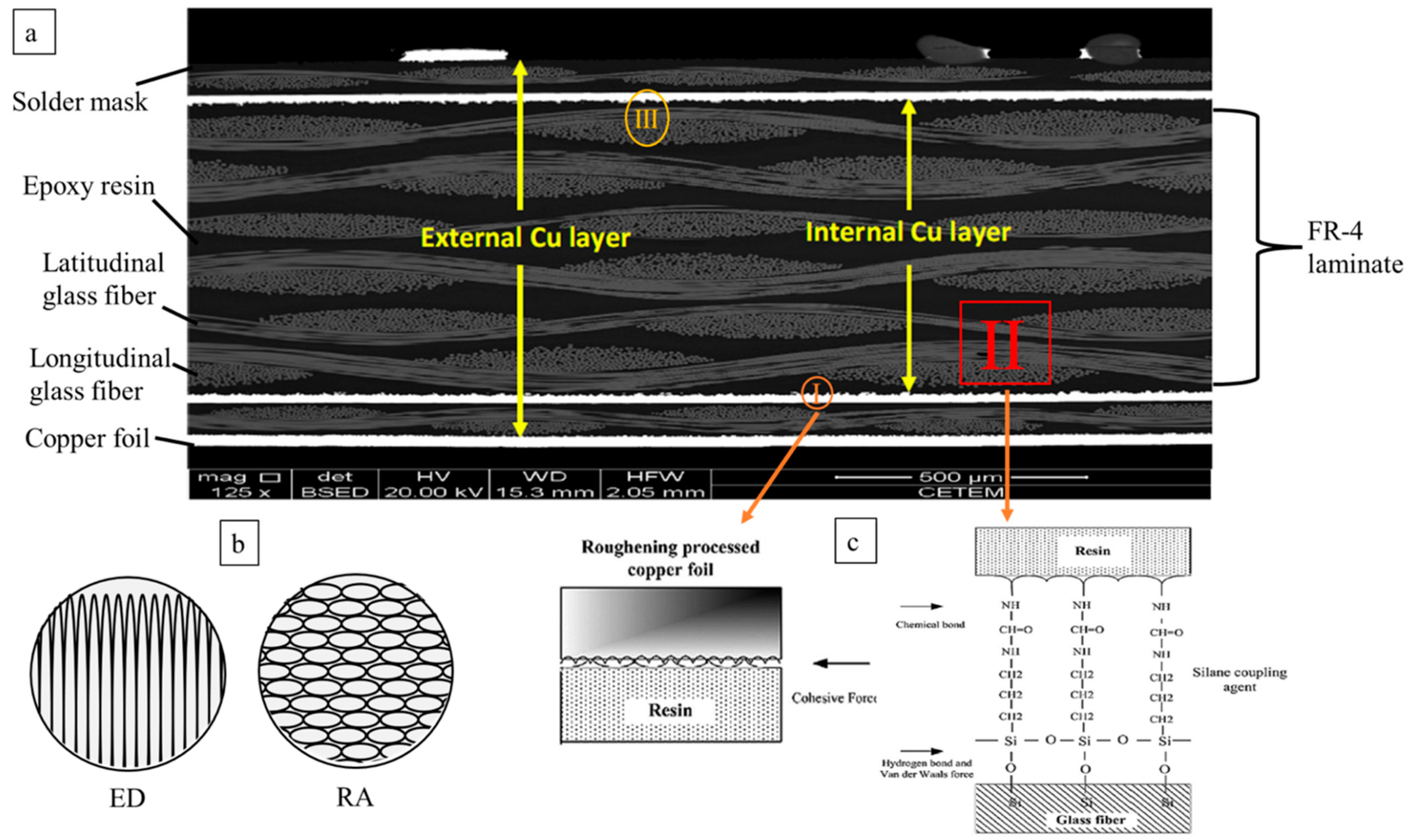
As the essence of every EEE, printed circuit boards (PCBs) form about 2% of the generalised e-waste composition and are one of the most valuable e-waste components that attract research interest and industrial applications to perform value recovery operations [5]. In general, PCBs are composed of 40% metals, 30% plastics and 30% ceramics, whereby these heterogeneous compositions form the sandwiched-structure of PCBs (Figure 1 and Figure 2). Base metals (copper, nickel, zinc, aluminium) and precious metals (gold, silver, platinum and palladium) are typically found in PCBs, and copper is the main metallic component. The typical copper content is about 10-fold higher compared to the respective metal ores [6]. Similarly, the gold content in PCBs ranges from 140 to 700 g/t, which is much higher than the average gold grade in gold ore deposits [7]. The presence of these valuable metals drives the economics of e-waste recycling. The extraction of critical metals, such as rare earth elements from e-waste (e.g., fluorescent lamp phosphors, hard disk drives), is primarily limited to lab studies and is not extensively adopted at the industrial scale [8].
Considering the common structure of PCBs, the multiple layers of glass fibre and copper clads are held together by brominated epoxy resin (BER), which contains brominated flame retardants (BFRs) (Figure 2). The addition of BFRs enables the flame retardancy properties of PCBs, which, on the other hand, also raises safety concerns due to the formation of toxic by-products during informal and formal recycling activities (Section 2.3). This aspect, in conjunction with the presence of heavy metals (e.g., lead), does not recommend PCB landfilling considering the potential adverse environmental and human health effects. Considering social aspects, e-waste management methodologies significantly vary between developed and developing countries. At the same time, transboundary movement of e-waste from the USA and Europe to developing countries in Asia and Africa is also reported and it also exerts an additional burden on the local e-waste management practices in developing countries [3].
In addition, informal or artisanal e-waste based value recovery operations are not recommended, as these value recovery operations are typically employed in developing countries despite health and safety risks to humans and environmental impacts [3,9]. The high concentration of flame retardants detected in the samples of soil, air, water and sediments obtained from informal e-waste processing sites elucidate the seriousness of the environmental pollution [10]. This implies the urgent requirement for organised and sustainable e-waste management (i.e., employ extended producer responsibility or EPR schemes to collect e-waste) and value recovery operations, especially in developing countries [11].
Figure 2.
(a) Microscopic view of PCBs internal structure—Reproduced from [12] with permission from Waste Management, (b) grain structure of electro-deposited (ED) copper foils and rolled annealed (RA) copper foils [13], (c) hetero-component interfaces: (I) copper foil–epoxy resin (II) epoxy resin-glass fibre cloth interface (epoxy-GFC) (III) copper foil-glass fibre cloth interface (copper foil—GFC)—Reproduced from [14] with permission from Journal of the Air and Waste Management Association.

Pyrometallurgical, hydrometallurgical and integrated pyro-hydrometallurgical techniques are employed in formal and semi-formal value recovery operations, though hydrometallurgy based operations are the norm in developing countries [3,15,16,17]. Metal extraction through various hydrometallurgical routes has been extensively investigated, and PCB pre-treatment operations (i.e., dismantling, size reduction, metal separation) are invariably performed prior to the hydrometallurgical methods. Comminution operations are energy intensive and the conventional PCB size reduction techniques (e.g., crushing, shredding followed by milling) result in particles in the order of tens of microns and smaller. The manipulation of the extent of comminution or degree of metal liberation by other means [18] could improve the overall economic feasibility of hydrometallurgical techniques (i.e., reduce energy costs during comminution). The production of coarse PCB particles (e.g., 1–3 cm), while eliminating the conventional milling step, is thus considered as a potential pre-treatment method pertaining to hydrometallurgy based e-waste value recovery. This niche area in e-waste recycling is not extensively studied.
Coarse PCB particle pre-treatment techniques thus focus on weakening the PCB structure [19,20,21] by removing different components of PCBs, such as solder mask [22,23] and BERs [24,25,26,27,28]. To prevent the overgrinding of PCBs, size reduction with a shearing principle, such as cutting, is preferred as these techniques are more effective and less energy intensive. The dust generation is also suppressed [9,29]. The resultant coarse PCB particles should be subjected to subsequent pre-treatment operations to separate the metal fraction. Since this burgeoning area of research is not yet well studied, the objective of this work is to analyse suitable coarse PCB particles’ pre-treatment mechanisms to produce metal fractions prior to hydrometallurgy based metal extraction and recovery operations.
2. PCBs
2.1. Populated and Unpopulated PCBs
2.2. Internal Structure of PCBs
The application of coarse PCB particles’ pre-treatment techniques depends on the internal structure of PCBs. FR-4 is a composite material, which comprises thermosetting epoxy resin reinforced with woven glass fibre (Figure 2a). The glass fibre used in PCBs belongs to the category of E-glass, and SiO2, CaO, Al2O3 and MgO are the main constituents of E-glass [31]. FR-4 is the most widely used PCB core material with enhanced end-use properties, though the individual constituents have different physical and chemical properties (Table 1). Copper foils are laminated on both sides of FR-4, forming a copper clad laminate.
Copper foil is used as the primary conductive material in PCBs due to its excellent electrical conductivity properties. Electrodeposited (ED) and rolled annealed (RA) copper foils are the two main copper foils used in PCBs manufacturing (Figure 2b) [31]. The grain structure formed during this copper foil manufacturing technology is significantly different, with a vertical grain structure for ED copper foils (Figure 2b), and a horizontal grain structure for that of RA copper foils (Figure 2b) [13]. Typically, ED copper foil has a rougher surface as compared to RA copper foils [32]. The rough surface of ED copper foils enhances bonding with epoxy resin systems (Figure 2c) [31].

Table 1.
Key properties of different components of PCBs. Reproduced from [33] with permission.
Table 1.
Key properties of different components of PCBs. Reproduced from [33] with permission.
| Components of PCBs | Elastic Modulus, GPa | Tensile Strength, MPa | Coefficient of Thermal Expansion (CTE), 10−6/°C | Dielectric Constant at 10 GHz |
|---|---|---|---|---|
| Epoxy-cyanate blended resin | 3.3 | 61 | 20 | 2.80 |
| E-glass, D450 1080 weave | 72 | 789 | 5.4 | 6.88 |
| Laminate board, 2 layers 1080 fabric (48.4% glass) | 29 | 415 | 12 | 3.93 |
As a reinforcement phase, glass fibre provides mechanical strength and stiffness to the composite material due to the higher tensile strength and elastic modulus (Table 1). The durable epoxy-GFC bonds ensure the high mechanical strength of the composite material. Coupling agents are applied to glass fibre to enhance the adhesion to the epoxy resin (Figure 2c) [14,31]. When a load is applied on PCBs, the load is transferred from the epoxy resin system to the reinforcement phase via the epoxy resin-GFC interface. Without the reinforcement phase, the structural integrity of PCBs is rather ineffective. Nevertheless, the ultimate strength of PCBs is not only dependent on the intrinsic strength of glass fibre; factors such as weaving patterns and the number of fabric layers also influence the composite strength of PCBs [34].
The epoxy resin systems of FR-4 comprises difunctional, tetrafunctional and multifunctional epoxy resins, which are defined based on the number of epoxide functional groups [31]. The increase in the number of cross-linking sites (i.e., functional groups) allows greater cross-linking density. Additives, such as the curing agents, are added to the epoxy resin system to enhance cross-linking and polymerisation in the resin [31]. As the degree of cross-linking increases, the glass transition temperature of the epoxy resin system increases [35]. is defined as the temperature at which material transforms from rigid to rubbery [31,36]. Thus, heating beyond causes changes in material properties (e.g., Young modulus, CTE), and influences thermal shock pre-treatment (Section 3.1.1) [31,37].
2.3. BFRs and Dioxins
More than 175 different types of flame retardants are available in the market, among which at least 75 of them are BFRs [38]. Polybrominated diphenyl ethers (PBDEs), tetra-bromobisphenol A (TBBP-A) and hexabromocyclododecane (HBCD) are among the three categories of BFRs that have been well-researched on [39,40,41]. Bromine is used in BFRs due to the effectiveness of this halogen in capturing the free radicals, hence suppressing the combustion [40].
In the manufacturing of PCBs, the fire retardancy property of the PCBs is achieved by brominating the epoxy resin with TBBP-A [31]. Following the usage restrictions of PBDEs in the “RoHS directive (2011/65/EU)” by the European Commission, TBBP-A is the most widely used BFR [42]. Approximately 90% of TBBP-A is used in the production of epoxy and polycarbonate resin [39,40], and the typical bromine composition in TBBP-A is approximately 59% [31].
BFR is the primary source of bromine in Br-containing dioxin and furans [43]. Polybrominated dibenzo-p-dioxins and dibenzofurans (PBDD/Fs) and mixed polybromochloro-dibenzo-p-dioxins and dibenzofurans (PXDD/Fs) are among the most noxious thermal by-products that could form, especially during the recycling of BFRs containing products [41,44,45]. Both controlled incineration and uncontrolled combustion and burning of PCBs could potentially lead to the formation of PBDD/Fs and PXDD/Fs [46]. The possible PBDD/Fs and PXDD/Fs formation routes can be further categorised into precursor formation, De novo formation and the inefficiency in the destruction of BFRs, which contains PBDD/Fs [46].
3. Coarse PCB Particles’ Pre-Treatment Techniques
One of the key factors to be considered in the development of suitable coarse PCB particles’ pre-treatment techniques is the heterogeneity in the composition of WPCBs [9]. Since milling is not applicable in coarse PCB particles’ pre-treatment techniques, it is not discussed in this work. Upon physical, chemical, electrical and thermal pre-treatment techniques, the embedded inner copper layers in the sandwiched-structure of PCBs should be liberated, and thus the separation of metal and non-metal fractions can be achieved. The utilisation of thermal pre-treatment [37,47,48] and organic solvent [19] prior to comminution enhances the liberation between metal and non-metals. This could alleviate the overall operational expenses during coarse PCB particles’ pre-treatment.
3.1. Thermal Pre-Treatment Techniques
3.1.1. Thermal Shock
The thermal expansion mismatch between different components of PCBs (i.e., epoxy resin, glass fibre and copper foil—Table 1) creates a thermal shock, which easily facilitates the comminution of laminated materials [14,37]. Under a drastic temperature change (either heating or cooling), the structural deformation of PCBs results in, which is reflected by the significant reduction in mechanical properties (i.e., tensile and flexural strength) [14,48]. A multitude of other studies that performed cryogenic crushing on PCBs also corroborates this finding [14,49,50,51].
The pre-treatment of coarse PCBs via heating is performed in a tubular furnace [14,37] and steam reactor [48] to pre-weaken the interfacial bonding (Figure 3). These studies performed heating at the temperature range of 200–270 °C to avoid pyrolysis. However, Liu et al. [37] set the peak temperature at 300 °C due to the discrepancies in identifying the onset temperature of pyrolysis. Li et al. [52] also elucidated the difference in pyrolysis onset temperature, which ranges from 270–350 °C due to the analytical methods and conditions. Affirmative results are obtained on the reduction of energy consumption [48] and noise pollution [14] during comminution.
The microstructure evolution at the interfaces is observed and vivid images of structural deformation are also illustrated [14,37,48,53]. The detachment of epoxy resin from the copper foil is observed, possibly due to the cohesive force failure during thermal shock pre-treatment (Figure 2c) [14,37]. Moreover, the broken hydrogen bond and the ineffective van der Waals forces, in enhancing linking between the layers, cause cracks at the epoxy-GFC interface (Figure 2c) [14,37]. These factors initiate the delamination of PCBs.
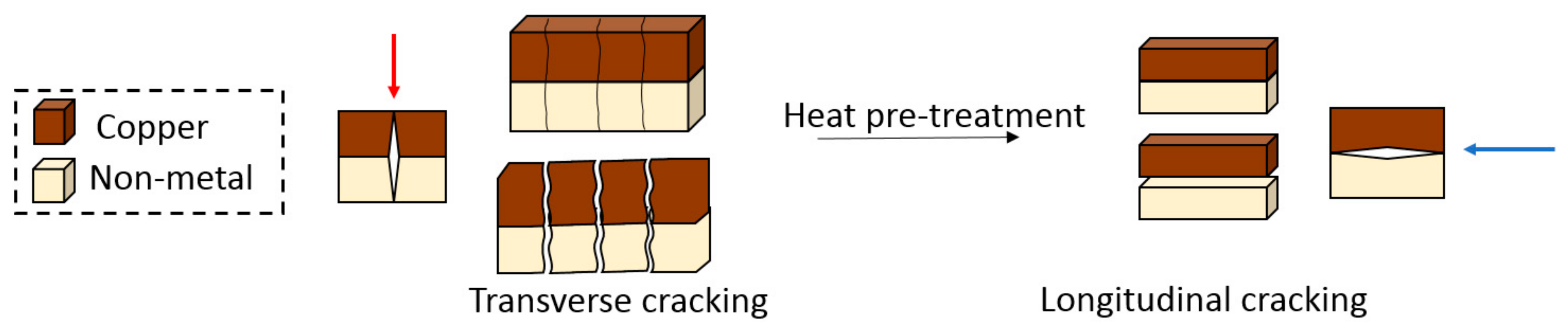
Besides that, the cracking mode is altered from transverse cracking to longitudinal cracking once PCBs are heat-treated prior to comminution (Section 3.2) [53]. PCBs that are treated with residual steam pre-processing showed similar results under the three-point bend test [48]. Chen et al. [48] also discussed the modification of physical and chemical properties of epoxy resin (i.e., cross-linking agent) when the temperature surpasses , which ultimately leads to the instability and structural deformation of PCBs. This irreversible destruction of PCBs’ structure significantly reduces the mechanical properties (i.e., tensile and impact strength) of PCBs. Peel resistance, which is an indicator of the adhesiveness between copper foil and insulator (i.e., epoxy resin and glass fibre), is reported to be lower for the case of heat-treated PCBs. This indicative aspect shows the effectiveness of liberation [48].
Other than the failure mechanisms attributed to the inherent properties of PCBs, the moisture absorbed onto the PCBs that vaporises upon heating is propitious to the liberation of the interfaces [37]. In addition, the thermal strain that is trapped in the PCBs during PCB manufacturing can also lead to PCBs deformation [54]. A multitude of other studies also corroborated this finding and highlighted the failure of the PCBs during alternating adoption of heating and cooling due to the creation of thermal residual stress [34,37,55,56]
Liu et al. [37] surmised that the thermal shock pre-treatment is a potential alternative for metal recovery without undergoing comminution, as copper foil can be easily separated from the substrate by using a hand, though this is not reported or recommended at the industrial scale.

3.1.2. Pyrolysis
Conventionally, the pyrolysis of WPCBs has been performed in a nitrogen atmosphere at a temperature range of 300–800 °C [57,59,60,61,62]. These studies are commonly carried out in a fixed bed reactor. TGA tests are performed to predict the pyrolysis condition of WPCBs over different temperatures (Figure 3). The most appropriate pyrolysis temperature is selected upon considering the weight loss of PCBs and energy consumption [63]. Wang et al. [63] selected 700 °C as the pyrolysis temperature, as a further increase in temperature would not result in an obvious weight loss.
Pyrolysis is typically employed due to its energy conversion efficiencies and less severe environmental impacts as compared to combustion/incineration [64,65,66,67].
Since pyrolysis is operated at a relatively lower temperature compared to smelting, the organic materials (i.e., epoxy resin) are decomposed into flammable gases and liquid tar whereby these by-products can be reused as fuel for the pyrolysis process [67,68]. The decomposition of organic materials is represented by the weight loss during pyrolysis and is responsible for the structural damage of PCBs [67,69].
The typical distribution of pyrolysis products is 71–72 wt% solid residue, 18–21 wt% tar and 6–10 wt% gas [57,70]. The distribution of these products in three phases is affected by the temperature, residence time and reactor type [71]. These parameters can be altered to meet the required pyrolysis product yield.
Pyrolysis has been performed on PCBs with large particle sizes (i.e., 2 cm × 1.5 cm) without further comminution into smaller sizes [72]. The resultant solid residue (i.e., metals and glass fibre) can be separated easily [57,63,67]. At the same time, the solid residue composes of metal and glass fibre that is left unaltered during pyrolysis, with the dimensions equal to the untreated PCBs [59,73] (Figure 4a). These solid residues (Figure 4a,b) are subjected to crushing and physical separation prior to conventional hydrometallurgy [67,68,73,74]. This size reduction is expected to consume less energy due to the loss of the structural integrity of PCBs.
Alternatively, the resultant pyrolysis solid residues could be used for subsequent coarse PCB particles’ pre-treatment and metal extraction flowsheets, though this is not extensively discussed in the literature.
Chen et al. [67] explored the effect of coarse PCBs’ particle size and pyrolysis temperature on metal recovery and concluded that the energy consumption is significantly reduced by nearly 50% when the optimised parameters (i.e., 4 cm PCB pieces: large particle size and 330 °C: lower pyrolysis temperature) are selected.
Different forms of pyrolysis are investigated, especially vacuum pyrolysis and microwave-induced pyrolysis. The latter was found to be more efficient [69,75]. Huang et al. [69] performed comparison studies between microwave-induced pyrolysis and conventional pyrolysis. A greater weight loss of PCBs and delamination extents was achieved by microwave-induced pyrolysis of PCBs and it resulted in higher metal recovery. Huang et al. [69] surmised that microwave-induced pyrolysis could be a potential substitution to replace conventional comminution processes prior to hydrometallurgical processes since 96% copper extraction efficiency can be achieved using large particle sizes (i.e., 3.1 cm × 2.4 cm). However, further studies are required to compare the metal liberation efficiency for both microwave-induced pyrolysis and conventional comminution to validate the aforementioned finding.
Disadvantages of pyrolysis: During pyrolysis, HBr and organobrominated compounds are formed due to the debromination of BFR [68,71]. The decomposition of organic materials in the absence of oxygen occurs during pyrolysis. Dioxin generation is significantly reduced, which is much lower than the permissible limits [74]. However, the liquid product of pyrolysis (i.e., tar) may contain the precursors for the dioxin formation, which restricts the reusability of those as fuel though the high heating value [71].
The temperature range for the dioxin formation is seldom reported, but dioxin formation is reported at pyrolysis temperatures of 600 °C and 850 °C [62]. This implies that the temperature for dioxin formation is aligned with certain pyrolysis operating conditions, and the pyrolysis of PCBs could form dioxins, though it is not explicitly measured. Engineering solutions, such as the use of calcium carbonate and alkali pre-treatment, can be implemented to remove dioxin precursors [70]. An NaOH scrubber can also be installed as a post-pyrolysis treatment to remove the emission of HBr into the environment [76].
3.2. Mechanical/Physical Pre-Treatment Techniques
Crushing plays a vital role in PCBs recycling as this physical process influences metal liberation, grade and recovery [47]. The crushing process pertaining to the generation of coarse particles should yield enough metal liberation from the non-metal fraction to facilitate subsequent leaching reactions [19,47]. A higher degree of metal liberation can be achieved by reducing the particle size, though excessive comminution generates large amounts of fine particles, which is contrary to the objective [77,78]. Meanwhile, inadequate crushing paves to poor metal liberation, which adversely affects the metal recovery [18]. A multitude of other studies (e.g., [78,79,80]) corroborated these findings and identified comminution as an appropriate size reduction technique.
Prestele [20] discussed the excessive use of energy in the conventional mechanical size reduction process by quantifying the energy demand and evaluated the extent of comminution that is necessary for the manifestation of efficient metal extraction.
PCBs possess high hardness and strength values (Section 2.2 and Table 1). Shearing force or impact force is preferable to yield a coarse size reduction of these multi-layered composites [20]. Cutting of PCBs into a regular shape and size (i.e., 1 cm × 1 cm) thus employs a shearing mechanism and can be performed manually using a shear cutter [36], band saw [21] and guillotine. During the size reduction process of PCBs, the non-metallic fraction suffers from brittle fracture failure more readily than the metallic fraction [9,81]. However, the applied shredding process would not fully expose the outer copper layers. In addition, the delamination of the inner copper layers was not very effective considering the accessibility of lixiviants [20]. It is also reported that the metal content is distributed unevenly in different size fractions [19].
When coarse PCB particles are prepared by comminution (i.e., no prior pre-weakening), a complete metal liberation would not be expected since the resultant PCBs are formed by different components/materials (e.g., silkscreen, solder mask, solders, metal layers and substrate) [82]. Evidently, the shredded or crushed PCB pieces are still attached to the solder mask and glass fibre (Figure 5).
Zhou et al. [51] performed coarse crushing of PCBs under cryogenic conditions (i.e., after pre-weakening). At –30 °C, PCBs are reported to be brittle. Thus, those can be crushed easily using a double roll crusher, generating crushed particles with a size fraction of 2 cm [51].
On the other hand, the cracking mode is altered from transverse cracking to longitudinal cracking once the PCBs are heat-treated prior to comminution (Figure 6) [53]. It is presumed that the shear forces induced by a universal crusher in the longitudinal direction surpass the pre-weakening bonding force at the PCB interface after the heat treatment, which causes the de-bonding of PCBs [53].
Rodrigues et al. [12] also employed pre-weakening effects of 2 cm PCB fragments by generating cracks with a jaw crusher to enhance metal leaching. The internal cracks introduced within the internal structure of PCBs facilitated the accessibility of lixiviant to the internal copper layers.
The cut PCBs pieces can be used in subsequent chemical treatments to investigate the effects on metal extraction under varying sizes. Moyo et al. [21] discerned that effective metal liberation can be achieved by applying different combinations of pre-treatment methods (e.g., cutting of PCBs and solder mask removal), which do not rely on heavily mechanised equipment.
3.3. Chemical Pre-Treatment Techniques
3.3.1. Solder Mask Removal
During PCB manufacturing, a solder mask is added to protect the metal layers from oxidation, though it hinders the metal exposure to the lixiviants in WPCBs recycling [22,23,25]. This chemical coating or the lacquer layer must be removed from the coarse particles prior to metal extraction processes using coarse PCB pieces (Figure 7).
Rodrigues et al. [12] reported the concomitant increase in copper extraction efficiency (about 40%) with the lacquer layer removed WPCBs, as compared to the original WPCBs, and the exposed external copper layers resulted in improved leaching efficiency. However, the solder mask removal method depends on the type of PCB. In addition, it may not fully pre-treat the coarse PCB particles as in multi-layered PCBs (i.e., internal copper layers are not affected).
A strong alkali, such as sodium hydroxide (NaOH), was employed to remove the solder mask from the surface of PCBs under varying conditions (i.e., concentration of reagents, PCBs size, duration and temperature) [21,22,23]. A mixture of potassium hydroxide (KOH) and diethylene glycol was also adopted [12]. Though this chemical pre-treatment step has been commonly performed on coarse PCB particles, the effectiveness of the reagents in the removal of solder mask under optimised conditions is seldom discussed.
3.3.2. Organic Swelling
BERs that firmly bind metal layers and glass fibre together complicate PCB delamination (i.e., separation of layers from the PCB laminate), and those can be removed with organic swelling mechanisms [9]. When coarse PCB pieces are treated with organic solvents, structural damage initiates, which slowly leads to the delamination of PCBs. This is due to the difference in the CTE of PCBs material composition and the reaction between the BERs and the organic solvent [19].
Due to the reagent regeneration ability, various organic solvents were investigated. Those were dimethyl sulfoxide (DMSO) [83], dimethylformamide (DMF) [25,36,84], N-methyl-2-pyrrolidone (NMP) [24] and dimethylacetamide (DMAc) [19,28]. However, these studies mainly focused on the detection of removed/dissolved BERs from the PCBs present in the organic solvents, using various characterisation techniques, and then employed organic reagent regeneration ability after the treatment [24,25,28,84]. The change in the properties of PCBs and the effectiveness of this organic swelling pre-treatment on metal extraction is seldom discussed and more research studies are required to ascertain the underlying layer delamination mechanisms.
Organic swelling based PCBs delamination is integrated with ultrasonic bath [25,84] and microwave treatment [85], and it is supposed that the layer separation time is reduced. In addition, PCBs delamination is successfully executed at a low temperature (50 °C) when ultrasonic treatment is applied, though the layer separation time is expected to be longer as compared to conventional organic swelling treatment, the operating temperature of which is commonly high (135–160 °C) [25,28].
Organic solvent (e.g., DMAc) is heated together with coarse PCB pieces [19] since mechanical pre-treatment is ineffective at liberating metals of relatively coarse size particles [86]. At 100 °C, Han et al. [19] reported no delamination of PCBs as the heating temperature is lower than the of BERs (i.e., 135 °C). However, the mechanical properties of PCBs are significantly altered as noticeable cracks and interfacial destruction were observed. Han et al. [19] proposed the underlying organic swelling mechanisms. Firstly, during heating, the higher expansion rate of BERs compared to copper causes the copper layer to suffer from an internal expansion force. Secondly, DMAc molecules accelerate and penetrate into the pores generated by non-metal thermal expansion. This also stimulates an internal expansion force, which weakens the interfacial bonding force. Thirdly, cracks are induced at the metal and non-metal interface and it results in layer separation.
The solder mask removal during organic swelling pre-treatment is also discussed [25,36]. The separation of the solder mask is also achieved during the delamination step, whereby the solder mask remains intact with the glass fibre. However, Verma et al. [28] presented the hindrance caused by the solder mask during the organic swelling process. The synergistic effect of both pre-treatment methods (i.e., solder mask removal and organic swelling) on leaching efficiency is not yet explicitly discussed in the literature.
This organic swelling method is deemed to be a promising method due to its high recyclability rate, high organic reagent regeneration, relatively less energy consumption for heating and zero dust generation. However, the choice of solvents is significant for ensuring the commercial viability of this pre-treatment method. The high specific heat and viscosity properties for both DMSO and NMP, as compared to DMF, result in excessive energy consumption in heating and obstruction in mass transport [87,88]. Moreover, DMSO could penetrate through human skin, whereas NMP is carcinogenic and is detrimental to the human reproductive system [36]. The installation of special ventilation systems and the implementation of more stringent safety measures are needed to ensure safe organic swelling operations. Though both DMF and DMAc are appraised in terms of safety and stable operation near the boiling points, the performance of DMAc in resin dissolution is 20% better than that of DMF [26]. DMAc is thus more preferable and Verma et al. [27] employed it for subsequent optimisations of organic swelling experiments.
3.4. Electrical Pre-Treatment Techniques
A significant metal liberation can also be achieved when coarse PCBs are treated with high voltage electrical pulse (HVEP) comminution. The use of electro dynamic fragmentation in the pre-treatment of PCBs is analogous to the HVEP comminution [89]. HVEP comminution does not result in size reduction to a greater extent since most of the applied electrical energy is allocated at the hetero-component interface for delamination (Figure 2). The resultant particles are thus concentrated at a narrow size fraction (i.e., especially copper in the coarse fraction), which eases the subsequent metal extraction processes. A better liberation efficiency is observed in HVEP comminution as compared to conventional mechanical crushing, and also results in a reduced fine particle fraction due to the pre-weakening or pre-destruction effects [78,90]. This helps to mitigate the loss of valuable materials.
In HVEP comminution, size reduction is achieved by the generated shock waves. The crushing effect of PCBs can be controlled by manipulating the voltage and the pulse number [86]. With a uniform electrical field, the breakdown is most likely to occur at the copper foil-GFC interface due to the differences in electrical properties [78].
Comparison studies are performed to investigate the crushing impacts of HVEP comminution and hammer mill [89]. Delamination is observed on HVEP-treated PCBs with a negligible size reduction effect, which is absent for the hammer mill products. On the other hand, the applied energy during HVEP comminution is primarily attributed to the copper foil-GFC interface as compared to the GFC-GFC interface, and this is evidently proven by the larger alteration in the bending strength at the copper foil-GFC interface after HVEP comminution [86]. This implies that selective crushing based on the interface material could be achieved.
Duan et al. [86] explained the liberation mechanisms of HVEP using the energy band theory, which can be divided into four stages: (1) HVEP causes electrons to approach copper foil-GFC interface, forming an electrons array at the interface; (2) internal breakdown begins when more electrons arrive at the copper foil-GFC interface under the increased electrical potential; (3) conductive channels are generated at the copper foil-GFC and GFC-GFC interfaces, which ultimately form electrical tree growth that propagates at the interfaces and between the layers; (4) copper is favourably liberated at the copper foil-GFC interface. In addition, PCB rupture is also caused by crack propagation due to the compression and tensile waves generated by different PCB components (e.g., copper, GFC and epoxy resin) through reflection and refraction [78]. Besides that, the high-temperature environment created during HVEP comminution causes copper to melt and decompose the epoxy resin, which eventually contributes to the easier separation of copper foil and GFC.
Martino et al. [89] performed HVEP comminution using populated motherboards and reported the sequential damage on the boards under increased electrical energy (Table 2).
This technique thus possesses the added advantage of electrical component removal in advance, which is one of the requirements for hydrometallurgical operations. Moreover, secondary pollution due to dust can be avoided when the breakage of PCBs takes place in water. Besides that, SEM images showing the corroded edges of copper layers after HNO3 leaching are presented and the acid leaching is improved due to the structural opening caused by HVEP comminution [89].
The main disadvantage of HVEP comminution is the high energy costs, which correlates to the high operating costs (Table 2) in industrial PCBs recycling. For a similar degree of metal liberation, HVEP stage 2 consumes 38 times more energy compared to the hammer mill comminution (i.e., 23 kWh/t) [89].
4. Development of Coarse PCB Particles Based Flowsheets
4.1. Conventional Flowsheets for PCBs Pre-Treatment
In conventional PCB pre-treatment processes for hydrometallurgical operations, many flowsheets are already developed with the amalgamation of wet and dry processes to separate metals from non-metallic components. In these conventional flowsheets, crushing/shredding and milling are employed to increase the degree of metal liberation. Separation of metals and non-metals are achieved using physical separation techniques, such as magnetic, electrostatic and gravity separation (Figure 8).
Even though the milling process registers high metal extraction efficiencies, energy costs are invariably high, and dust and noise pollutions are also drawbacks [91]. Coarse PCB pieces based pre-treatment flowsheets that avoid milling can be developed, though this niche aspect is not extensively addressed in the e-waste recycling literature.
4.2. New Flowsheets for Coarse PCBs Pre-Treatment
The elimination of PCBs milling from the conventional PCBs pre-treatment flowsheets and the use of coarse PCB particles’ pre-treatment techniques could enhance the economic feasibility of hydrometallurgical processes, especially in developing countries. It is expected that coarse PCB particles based flowsheets consume less energy as they avoid energy intensive PCB milling operations in conventional PCB pre-treatment flowsheets. In addition, this could provide pathways to utilise the separated non-metallic fraction efficiently.
Based on the detailed analysis of coarse PCB particles’ pre-treatment techniques considering the key factors, such as the extent of delamination, energy consumption and environmental impacts (Table 3—only qualitative comparison was performed due to data unavailability in the literature), three potential flowsheets are formulated in this work and those are illustrated in Figure 9. In the proposed flowsheets, coarse PCB particles (in the order of a few centimetres) are produced by employing a shearing mechanism, since it is highly effective to obtain coarse PCB pieces.
Figure 9a illustrates a chemical pre-treatment oriented flowsheet, whereas the flowsheets in Figure 9b,c are developed using thermal pre-treatment (pyrolysis and thermal shock, respectively). During these chemical and physical pre-treatment processes, internal bonds breakage and layer separation occur to a certain extent and it is expected that the effects are greater in solder mask removal and organic swelling (Figure 9a) and the pyrolysis process (Figure 9b). Less extensive comminution could be required for thermally treated coarse PCB particles to increase the degree of layer separation after the thermal shock and is thus proposed in Figure 9c. Subsequently, in all the flowsheets, a mechanical action is employed to achieve full layer separation (i.e., complete layer separation without a less intense mechanical action is highly unlikely considering industrial processes and manual layer separation is also not practical). Based on the physical properties, metal and non-metal fractions separation is achieved (Figure 9) and the resultant metal fraction can be used in hydrometallurgical flowsheets and/or as a metal concentrate.
HVEP comminution based flowsheets are not suggested in this work due to relatively high energy costs, though this niche PCB treatment method would improve in the future.
The feasibility of the developed flowsheets will be tested in follow-up studies, including quantitative data, focussing on socio-techno-economic considerations. The identification of the limitations and further improvements for these flowsheets would ensure their effectiveness and practicality.
5. Conclusions
PCBs with heterogenous material compositions are currently pre-treated by crushing followed by milling to yield sub-millimetre size particles required for conventional hydrometallurgical operations, though the milling operations are extremely energy intensive. A shifting in research interests towards the investigation of pre-treatment methods employing coarse PCB pieces can be seen and the separated metal fraction without milling could be utilised in hydrometallurgical operations or as a metal concentrate. Analysis of thermal, chemical, mechanical and electrical pre-treatment techniques for coarse PCB particles reveals their advantages and disadvantages, and the combination of different pre-treatment techniques results in potential flowsheets for coarse PCB pieces. Several potential flowsheets were formulated in this work and the assessment of the suggested flowsheets needs to be performed considering social-techno-economic aspects through laboratory and pilot-scale studies.
In the wider context, continuous high generation of e-waste, improper waste management practices and informal PCBs based value recovery techniques pose notable adverse impacts to the environment and human health. This results in challenging conditions to achieve the sustainable development goals (SDGs) proposed by the United Nations [92]. The development of industrially applicable pre-treatment techniques for coarse PCB particles targeting formal and semi-formal value recovery operations in developing countries is of paramount importance to fulfil the SDGs, such as SDG 11 (Sustainable cities and communities) and SDG 12 (Responsible consumption and production). If coarse PCB particles-based pre-treatment techniques and flowsheets are economical compared to the conventional methods, e-waste management in urban communities can be optimised (i.e., SDG 11) and improved value recovery targets can be accomplished compared to the current levels (i.e., SDG 12).
Author Contributions
Conceptualization, I.M.S.K.I. and K.D.K.; methodology, K.D.K., I.M.S.K.I. and N.D.; resources, I.M.S.K.I.; writing–original draft preparation, K.D.K., I.M.S.K.I., N.D. and M.N.C.; writing–review and editing, K.D.K., I.M.S.K.I., N.D. and M.N.C.; supervision, I.M.S.K.I. and M.N.C.; project administration, I.M.S.K.I.; funding acquisition, I.M.S.K.I. and M.N.C. All authors have read and agreed to the published version of the manuscript.
Funding
This research was funded by the Fundamental Research Grant Scheme, Ministry of Education Malaysia (FRGS/1/2018/TK02/MUSM/03/1).
Data Availability Statement
The data presented in this study and the images added by the authors are available on request from the corresponding author.
Acknowledgments
The corresponding author acknowledges the funding provided by the Fundamental Research Grant Scheme, Ministry of Education Malaysia (FRGS/1/2018/TK02/MUSM/03/1).
Conflicts of Interest
The authors declare no conflict of interest. The funders had no role in the design of the study; in the collection, analyses, or interpretation of data; in the writing of the manuscript, or in the decision to publish the results.
References
- Huang, K.; Guo, J.; Xu, Z. Recycling of waste printed circuit boards: A review of current technologies and treatment status in China. J. Hazard. Mater. 2009, 164, 399–408. [Google Scholar] [CrossRef] [PubMed]
- Baldé, C.P.; Forti, V.; Gray, V.; Kuehr, R.; Stegmann, P. The Global E-Waste Monitor 2017: Quantities, Flows and Resources; United Nations University: Bonn, Germany; International Telecommunication Union: Geneva, Switzerland; International Solid Waste Association: Vienna, Austria, 2017. [Google Scholar]
- Ilankoon, I.M.S.K.; Ghorbani, Y.; Chong, M.N.; Herath, G.; Moyo, T.; Petersen, J. E-waste in the international context–A review of trade flows, regulations, hazards, waste management strategies and technologies for value recovery. Waste Manag. 2018, 82, 258–275. [Google Scholar] [CrossRef] [PubMed]
- Forti, V.; Balde, C.P.; Kuehr, R.; Bel, G. The Global E-Waste Monitor 2020: Quantities, Flows and the Circular Economy Potential. Available online: https://www.itu.int/en/ITU-D/Environment/Documents/Toolbox/GEM_2020_def.pdf (accessed on 16 April 2021).
- Widmer, R.; Oswald-Krapf, H.; Sinha-Khetriwal, D.; Schnellmann, M.; Böni, H. Global perspectives on e-waste. Environ. Impact Assess. Rev. 2005, 25, 436–458. [Google Scholar] [CrossRef]
- Hagelüken, C. Improving metal returns and eco-efficiency in electronics recycling-a holistic approach for interface optimisation between pre-processing and integrated metals smelting and refining. In Proceedings of the 2006 IEEE International Symposium on Electronics and the Environment, Scottsdale, AZ, USA, 8–11 May 2006; IEEE: Piscataway, NJ, USA, 2006; pp. 218–223. [Google Scholar]
- Kasper, A.C.; Veit, H.M. Gold recovery from printed circuit boards of mobile phones scraps using a leaching solution alternative to cyanide. Braz. J. Chem. Eng. 2018, 35, 931–942. [Google Scholar] [CrossRef] [Green Version]
- Dushyantha, N.; Batapola, N.; Ilankoon, I.M.S.K.; Rohitha, S.; Premasiri, R.; Abeysinghe, B.; Ratnayake, N.; Dissanayake, K. The story of rare earth elements (REEs): Occurrences, global distribution, genesis, geology, mineralogy and global production. Ore Geol. Rev. 2020, 122, 103521. [Google Scholar] [CrossRef]
- Ghosh, B.; Ghosh, M.K.; Parhi, P.; Mukherjee, P.S.; Mishra, B.K. Waste printed circuit boards recycling: An extensive assessment of current status. J. Clean. Prod. 2015, 94, 5–19. [Google Scholar] [CrossRef]
- Ge, X.; Ma, S.; Zhang, X.; Yang, Y.; Li, G.; Yu, Y. Halogenated and organophosphorous flame retardants in surface soils from an e-waste dismantling park and its surrounding area: Distributions, sources, and human health risks. Environ. Int. 2020, 139, 105741. [Google Scholar] [CrossRef]
- Kang, K.D.; Kang, H.; Ilankoon, I.M.S.K.; Chong, C.Y. Electronic waste collection systems using Internet of Things (IoT): Household electronic waste management in Malaysia. J. Clean. Prod. 2020, 252, 119801. [Google Scholar] [CrossRef]
- Rodrigues, M.L.M.; Leão, V.A.; Gomes, O.; Lambert, F.; Bastin, D.; Gaydardzhiev, S. Copper extraction from coarsely ground printed circuit boards using moderate thermophilic bacteria in a rotating-drum reactor. Waste Manag. 2015, 41, 148–158. [Google Scholar] [CrossRef]
- Coonrod, J. Bending, forming and flexing printed circuits. In Proceedings of the IPC Printed Circuits Expo, APEX Designers Summit, Los Angeles, CA, USA, 20–22 February 2007; Volume 1, pp. 594–615. [Google Scholar]
- Li, J.; Duan, H.; Yu, K.; Wang, S. Interfacial and mechanical property analysis of waste printed circuit boards subject to thermal shock. J. Air Waste Manage Assoc. 2010, 60, 229–236. [Google Scholar] [CrossRef] [Green Version]
- Tuncuk, A.; Stazi, V.; Akcil, A.; Yazici, E.Y.; Deveci, H. Aqueous metal recovery techniques from e-scrap: Hydrometallurgy in recycling. Miner. Eng. 2012, 25, 28–37. [Google Scholar] [CrossRef]
- Khaliq, A.; Rhamdhani, M.A.; Brooks, G.; Masood, S. Metal extraction processes for electronic waste and existing industrial routes: A review and Australian perspective. Resources 2014, 3, 152–179. [Google Scholar] [CrossRef] [Green Version]
- Yong, Y.S.; Lim, Y.A.; Ilankoon, I.M.S.K. An analysis of electronic waste management strategies and recycling operations in Malaysia: Challenges and future prospects. J. Clean. Prod. 2019, 224, 151–166. [Google Scholar] [CrossRef]
- Ruan, J.; Xu, Z. Constructing environment-friendly return road of metals from e-waste: Combination of physical separation technologies. Renew. Sustain. Energy Rev. 2016, 54, 745–760. [Google Scholar] [CrossRef]
- Han, J.; Duan, C.; Lu, Q.; Jiang, H.; Fan, X.; Wen, P.; Ju, Y. Improvement of the crushing effect of waste printed circuit boards by co-heating swelling with organic solvent. J. Clean. Prod. 2019, 214, 70–78. [Google Scholar] [CrossRef]
- Prestele, M.P. Assessment of a Shredding Technology of Waste Printed Circuit Boards in Preparation for Ammonia-Based Copper Leaching. Master’s Thesis, University of Cape Town, Cape Town, South Africa, 2020. [Google Scholar]
- Moyo, T.; Chirume, B.H.; Petersen, J. Assessing alternative pre-treatment methods to promote metal recovery in the leaching of printed circuit boards. Resour. Conserv. Recycl. 2020, 152, 104545. [Google Scholar] [CrossRef]
- Adhapure, N.N.; Dhakephalkar, P.K.; Dhakephalkar, A.P.; Tembhurkar, V.R.; Rajgure, A.V.; Deshmukh, A.M. Use of large pieces of printed circuit boards for bioleaching to avoid ‘precipitate contamination problem’and to simplify overall metal recovery. MethodsX 2014, 1, 181–186. [Google Scholar] [CrossRef]
- Jadhav, U.; Hocheng, H. Hydrometallurgical recovery of metals from large printed circuit board pieces. Sci. Rep. 2015, 5, 14574. [Google Scholar] [CrossRef] [Green Version]
- Wath, S.B.; Katariya, M.N.; Singh, S.K.; Kanade, G.S.; Vaidya, A.N. Separation of WPCBs by dissolution of brominated epoxy resins using DMSO and NMP: A comparative study. Chem. Eng. J. 2015, 280, 391–398. [Google Scholar] [CrossRef]
- Tatariants, M.; Yousef, S.; Sidaraviciute, R.; Denafas, G.; Bendikiene, R. Characterization of waste printed circuit boards recycled using a dissolution approach and ultrasonic treatment at low temperatures. RSC Adv. 2017, 7, 37729–37738. [Google Scholar] [CrossRef] [Green Version]
- Verma, H.R.; Singh, K.K.; Mankhand, T.R. Comparative study of printed circuit board recycling by cracking of internal layers using organic solvents-dimethylformamide and dimethylacetamide. J. Clean. Prod. 2017, 142, 1721–1727. [Google Scholar] [CrossRef]
- Verma, H.R.; Singh, K.K.; Mankhand, T.R. Liberation of metal clads of waste printed circuit boards by removal of halogenated epoxy resin substrate using dimethylacetamide. Waste Manag. 2017, 60, 652–659. [Google Scholar] [CrossRef]
- Verma, H.R.; Singh, K.K.; Mankhand, T.R. Delamination mechanism study of large size waste printed circuit boards by using dimethylacetamide. Waste Manag. 2017, 65, 139–146. [Google Scholar] [CrossRef]
- Yuan, Y. An Environmentally Benign Supercritical Fluid Process for Printed Wiring Board Recycling. Master’s Thesis, Texas Tech University, Lubbock, TX, USA, 2004. [Google Scholar]
- Chirume, B.H. Investigation of a Hydrometallurgical Process Route to Recover Metals from Waste Printed Circuit Boards. Master’s Thesis, University of Cape Town, Cape Town, South Africa, 2019. [Google Scholar]
- Coombs, C.F., Jr. Printed Circuits Handbook; McGraw-Hill Education: New York, NY, USA, 2008; ISBN 0071467343. [Google Scholar]
- Coonrod, J. Different copper foils for different reasons. The PCB Magazine, April 2012; 60–64. [Google Scholar]
- Longobardo, A. V Glass fibers for printed circuit boards. In Fiberglass and Glass Technology; Springer: New York, NY, USA, 2010; pp. 175–196. [Google Scholar]
- Wallenberger, F.T.; Bingham, P.A. Fiberglass and glass technology. In Energy-Friendly Compositions and Applications; Springer: New York, NY, USA, 2010. [Google Scholar]
- Chang, S.-S. Effect of curing history on ultimate glass transition temperature and network structure of crosslinking polymers. Polymer 1992, 33, 4768–4778. [Google Scholar] [CrossRef]
- Verma, H.R.; Singh, K.K.; Mankhand, T.R. Dissolution and separation of brominated epoxy resin of waste printed circuit boards by using di-methyl formamide. J. Clean. Prod. 2016, 139, 586–596. [Google Scholar] [CrossRef]
- Liu, F.; Wan, B.; Wang, F.; Chen, W. Effect of thermal shock process on the microstructure and peel resistance of single–sided copper clad laminates used in waste printed circuit boards. J. Air Waste Manage Assoc. 2019, 69, 1490–1502. [Google Scholar] [CrossRef] [PubMed]
- Birnbaum, L.S.; Staskal, D.F. Brominated flame retardants: Cause for concern? Environ. Health Perspect. 2004, 112, 9–17. [Google Scholar] [CrossRef]
- De Wit, C.A. An overview of brominated flame retardants in the environment. Chemosphere 2002, 46, 583–624. [Google Scholar] [CrossRef]
- Alaee, M.; Arias, P.; Sjödin, A.; Bergman, Å. An overview of commercially used brominated flame retardants, their applications, their use patterns in different countries/regions and possible modes of release. Environ. Int. 2003, 29, 683–689. [Google Scholar] [CrossRef]
- Shaw, S. Halogenated flame retardants: Do the fire safety benefits justify the risks? Rev. Environ. Health 2010, 25, 261–306. [Google Scholar] [CrossRef]
- Directive 2011/65/EU of the European Parliament and of the Council of 8 June 2011 on the Restriction of the Use of Certain Hazardous Substances in Electrical and Electronic Equipment (Recast). Off. J. Eur. Union. 2011, 32, 147–169.
- Watanabe, I.; Sakai, S. Environmental release and behavior of brominated flame retardants. Environ. Int. 2003, 29, 665–682. [Google Scholar] [CrossRef]
- Xiezhi, Y.; Markus, Z.; Magnus, E.; Anna, R.; Maria, L.; Hung, W.M.; Roland, W. E-waste recycling heavily contaminates a Chinese city with chlorinated, brominated and mixed halogenated dioxins. Organohalogen Compd. 2008, 70, 813–816. [Google Scholar]
- Markus, Z.; Yu, X.; Hung, W.; Roland, W. Fingerprints of chlorinated, brominated and mixed halogenated dioxins at two e-waste recycling sites in Guiyu/China. Organohalogen Compd. 2009, 71, 2263–2267. [Google Scholar]
- Zhang, M.; Buekens, A.; Li, X. Brominated flame retardants and the formation of dioxins and furans in fires and combustion. J. Hazard. Mater. 2016, 304, 26–39. [Google Scholar] [CrossRef] [PubMed]
- Duan, C.L.; Zhao, Y.M.; He, J.F.; Zhou, N.X. Research on liberation mechanism of the impact crushing waste printed circuit board. In Advanced Materials Research; Trans Tech Publications: Zurich, Switzerland, 2010; Volume 113, pp. 730–734. [Google Scholar]
- Chen, Y.; Li, J.; Duan, H.; Wang, Z. Thermal cracking of waste printed wiring boards for mechanical recycling by using residual steam preprocessing. Front. Environ. Sci. Eng. China 2011, 5, 167–174. [Google Scholar] [CrossRef]
- Koyanaka, S.; Endoh, S.; Ohya, H. Effect of impact velocity control on selective grinding of waste printed circuit boards. Adv. Powder Technol. 2006, 17, 113–126. [Google Scholar] [CrossRef]
- Yuan, C.Y.; Zhang, H.C.; McKenna, G.; Korzeniewski, C.; Li, J. Experimental studies on cryogenic recycling of printed circuit board. Int. J. Adv. Manuf. Technol. 2007, 34, 657–666. [Google Scholar] [CrossRef]
- Zhou, C.; Pan, Y.; Lu, M.; Yang, C. Liberation characteristics after cryogenic modification and air table separation of discarded printed circuit boards. J. Hazard. Mater. 2016, 311, 203–209. [Google Scholar] [CrossRef]
- Li, J.; Duan, H.; Yu, K.; Liu, L.; Wang, S. Characteristic of low-temperature pyrolysis of printed circuit boards subjected to various atmosphere. Resour. Conserv. Recycl. 2010, 54, 810–815. [Google Scholar] [CrossRef]
- Yan, G.; Guo, J.; Zhu, G.; Zhang, Z.; Zhao, P.; Xiangnan, Z.; Zhang, B. Liberation enhancement and copper enrichment improvement for waste printed circuit boards by heating pretreatment. Waste Manag. 2020, 106, 145–154. [Google Scholar] [CrossRef]
- Schuerink, G.A.; Slomp, M.; Wits, W.W.; Legtenberg, R.; Kappel, E.A. Modeling printed circuit board curvature in relation to manufacturing process steps. Procedia CIRP 2013, 9, 55–60. [Google Scholar] [CrossRef] [Green Version]
- Zeng, X.; Li, J.; Xie, H.; Liu, L. A novel dismantling process of waste printed circuit boards using water-soluble ionic liquid. Chemosphere 2013, 93, 1288–1294. [Google Scholar] [CrossRef]
- Ai, S.; Fu, H.; He, R.; Pei, Y. Multi-scale modeling of thermal expansion coefficients of C/C composites at high temperature. Mater. Des. 2015, 82, 181–188. [Google Scholar] [CrossRef]
- Guo, X.; Qin, F.G.F.; Yang, X.; Jiang, R. Study on low-temperature pyrolysis of large-size printed circuit boards. J. Anal. Appl. Pyrolysis 2014, 105, 151–156. [Google Scholar] [CrossRef]
- Cayumil, R.; Khanna, R.; Ikram-Ul-Haq, M.; Rajarao, R.; Hill, A.; Sahajwalla, V. Generation of copper rich metallic phases from waste printed circuit boards. Waste Manag. 2014, 34, 1783–1792. [Google Scholar] [CrossRef]
- De Marco, I.; Caballero, B.M.; Chomón, M.J.; Laresgoiti, M.F.; Torres, A.; Fernández, G.; Arnaiz, S. Pyrolysis of electrical and electronic wastes. J. Anal. Appl. Pyrolysis 2008, 82, 179–183. [Google Scholar] [CrossRef]
- Chiang, H.-L.; Lo, C.-C.; Ma, S.-Y. Characteristics of exhaust gas, liquid products, and residues of printed circuit boards using the pyrolysis process. Environ. Sci. Pollut. Res. 2010, 17, 624–633. [Google Scholar] [CrossRef] [PubMed]
- Chiang, H.-L.; Lin, K.-H. Exhaust constituent emission factors of printed circuit board pyrolysis processes and its exhaust control. J. Hazard. Mater. 2014, 264, 545–551. [Google Scholar] [CrossRef] [PubMed]
- Ortuño, N.; Conesa, J.A.; Moltó, J.; Font, R. Pollutant emissions during pyrolysis and combustion of waste printed circuit boards, before and after metal removal. Sci. Total Environ. 2014, 499, 27–35. [Google Scholar] [CrossRef] [PubMed] [Green Version]
- Wang, X.; Jiao, F.; Qin, W.; Li, Z.; Wang, N.; Liu, W.; Yang, C. Combination of pyrolysis and physical separation to recover copper and tin from waste printed circuit boards. JOM 2020, 72, 3179–3185. [Google Scholar] [CrossRef]
- Chen, Y.; Yang, J.; Zhang, Y.; Liu, K.; Liang, S.; Xu, X.; Hu, J.; Yao, H.; Xiao, B. Kinetic simulation and prediction of pyrolysis process for non-metallic fraction of waste printed circuit boards by discrete distributed activation energy model compared with isoconversional method. Environ. Sci. Pollut. Res. 2018, 25, 3636–3646. [Google Scholar] [CrossRef]
- Chen, Y.; Zhang, Y.; Yang, J.; Liang, S.; Liu, K.; Xiao, K.; Deng, H.; Hu, J.; Xiao, B. Improving bromine fixation in co-pyrolysis of non-metallic fractions of waste printed circuit boards with Bayer red mud. Sci. Total Environ. 2018, 639, 1553–1559. [Google Scholar]
- Gao, R.; Xu, Z. Pyrolysis and utilization of nonmetal materials in waste printed circuit boards: Debromination pyrolysis, temperature-controlled condensation, and synthesis of oil-based resin. J. Hazard. Mater. 2019, 364, 1–10. [Google Scholar] [CrossRef]
- Chen, Y.; Liang, S.; Xiao, K.; Hu, J.; Hou, H.; Liu, B.; Deng, H.; Yang, J. A cost-effective strategy for metal recovery from waste printed circuit boards via crushing pretreatment combined with pyrolysis: Effects of particle size and pyrolysis temperature. J. Clean. Prod. 2021, 280, 124505. [Google Scholar] [CrossRef]
- Hadi, P.; Xu, M.; Lin, C.S.K.; Hui, C.-W.; McKay, G. Waste printed circuit board recycling techniques and product utilization. J. Hazard. Mater. 2015, 283, 234–243. [Google Scholar] [PubMed]
- Huang, Y.-F.; Pan, M.-W.; Lo, S.-L. Hydrometallurgical metal recovery from waste printed circuit boards pretreated by microwave pyrolysis. Resour. Conserv. Recycl. 2020, 163, 105090. [Google Scholar] [CrossRef]
- Qiu, R.; Lin, M.; Qin, B.; Xu, Z.; Ruan, J. Environmental-friendly recovery of non-metallic resources from waste printed circuit boards: A review. J. Clean. Prod. 2021, 279, 123738. [Google Scholar] [CrossRef]
- Hsu, E.; Barmak, K.; West, A.C.; Park, A.-H.A. Advancements in the treatment and processing of electronic waste with sustainability: A review of metal extraction and recovery technologies. Green Chem. 2019, 21, 919–936. [Google Scholar]
- Ma, H.; Du, N.; Lin, X.; Li, C.; Lai, J.; Li, Z. Experimental study on the heat transfer characteristics of waste printed circuit boards pyrolysis. Sci. Total Environ. 2018, 633, 264–270. [Google Scholar] [PubMed]
- Long, L.; Sun, S.; Zhong, S.; Dai, W.; Liu, J.; Song, W. Using vacuum pyrolysis and mechanical processing for recycling waste printed circuit boards. J. Hazard. Mater. 2010, 177, 626–632. [Google Scholar] [CrossRef] [PubMed]
- Park, H.S.; Han, Y.S.; Park, J.H. Massive recycling of waste mobile phones: Pyrolysis, physical treatment, and pyrometallurgical processing of insoluble residue. ACS Sustain. Chem. Eng. 2019, 7, 14119–14125. [Google Scholar] [CrossRef]
- Yin, C. Microwave-assisted pyrolysis of biomass for liquid biofuels production. Bioresour. Technol. 2012, 120, 273–284. [Google Scholar] [CrossRef] [PubMed]
- Panda, R.; Pant, K.K.; Bhaskar, T. Efficient extraction of metals from thermally treated waste printed circuit boards using solid state chlorination: Statistical modeling and optimization. J. Clean. Prod. 2021, 313, 127950. [Google Scholar] [CrossRef]
- Xue, M.; Xu, Z. Computer simulation of the pneumatic separator in the pneumatic–electrostatic separation system for recycling waste printed circuit boards with electronic components. Environ. Sci. Technol. 2013, 47, 4598–4604. [Google Scholar] [CrossRef]
- Duan, C.L.; Diao, Z.J.; Zhao, Y.M.; Huang, W. Liberation of valuable materials in waste printed circuit boards by high-voltage electrical pulses. Miner. Eng. 2015, 70, 170–177. [Google Scholar] [CrossRef]
- Andres, U. Electrical disintegration of rock. Miner. Process. Extr. Metall. Rev. 1995, 14, 87–110. [Google Scholar] [CrossRef]
- Andres, U.; Timoshkin, I.; Jirestig, J.; Stallknecht, H. Liberation of valuable inclusions in ores and slags by electrical pulses. Powder Technol. 2001, 114, 40–50. [Google Scholar] [CrossRef]
- Koyanaka, S.; Ohya, H.; Lee, J.; Iwata, H.; Endoh, S. Impact milling of printed circuit board wastes for resources recycling and evaluation of the liberation using heavy medium separation. J. Soc. Powder Technol. Jpn. 1999, 36, 479–483. [Google Scholar] [CrossRef] [Green Version]
- Yoo, J.-M.; Jeong, J.; Yoo, K.; Lee, J.; Kim, W. Enrichment of the metallic components from waste printed circuit boards by a mechanical separation process using a stamp mill. Waste Manag. 2009, 29, 1132–1137. [Google Scholar] [CrossRef]
- Zhu, P.; Chen, Y.; Wang, L.Y.; Zhou, M.; Zhou, J. The separation of waste printed circuit board by dissolving bromine epoxy resin using organic solvent. Waste Manag. 2013, 33, 484–488. [Google Scholar] [CrossRef] [PubMed]
- Yousef, S.; Tatariants, M.; Tichonovas, M.; Bendikiene, R.; Denafas, G. Recycling of bare waste printed circuit boards as received using an organic solvent technique at a low temperature. J. Clean. Prod. 2018, 187, 780–788. [Google Scholar] [CrossRef]
- Monteiro, B.; Martelo, L.M.; Sousa, P.M.S.; Bastos, M.M.S.M.; Soares, H.M.V.M. Microwave-assisted organic swelling promotes fast and efficient delamination of waste printed circuit boards. Waste Manag. 2021, 126, 231–238. [Google Scholar] [CrossRef] [PubMed]
- Duan, C.; Han, J.; Zhao, S.; Gao, Z.; Qiao, J.; Yan, G. The stripping effect of using high voltage electrical pulses breakage for waste printed circuit boards. Waste Manag. 2018, 77, 603–610. [Google Scholar] [CrossRef] [PubMed]
- National Center for Biotechnology Information Dimethyl Sulfoxide. Available online: https://pubchem.ncbi.nlm.nih.gov/compound/Dimethyl-sulfoxide (accessed on 19 September 2021).
- National Center for Biotechnology Information 1-Methyl-2-pyrrolidinone. Available online: https://pubchem.ncbi.nlm.nih.gov/compound/1-Methyl-2-pyrrolidinone (accessed on 18 September 2021).
- Martino, R.; Iseli, C.; Gaydardzhiev, S.; Streicher-Porte, M.; Weh, A. Electro dynamic fragmentation of printed wiring boards as a preparation tool for their recycling. Miner. Eng. 2017, 107, 20–26. [Google Scholar] [CrossRef]
- Zhao, Y.; Zhang, B.; Duan, C.; Chen, X.; Sun, S. Material port fractal of fragmentation of waste printed circuit boards (WPCBs) by high-voltage pulse. Powder Technol. 2015, 269, 219–226. [Google Scholar] [CrossRef]
- Hino, T.; Agawa, R.; Moriya, Y.; Nishida, M.; Tsugita, Y.; Araki, T. Techniques to separate metal from waste printed circuit boards from discarded personal computers. J. Mater. Cycles Waste Manag. 2009, 11, 42–54. [Google Scholar] [CrossRef]
- The United Nations: The 17 Goals. Available online: https://sdgs.un.org/goals (accessed on 16 April 2020).
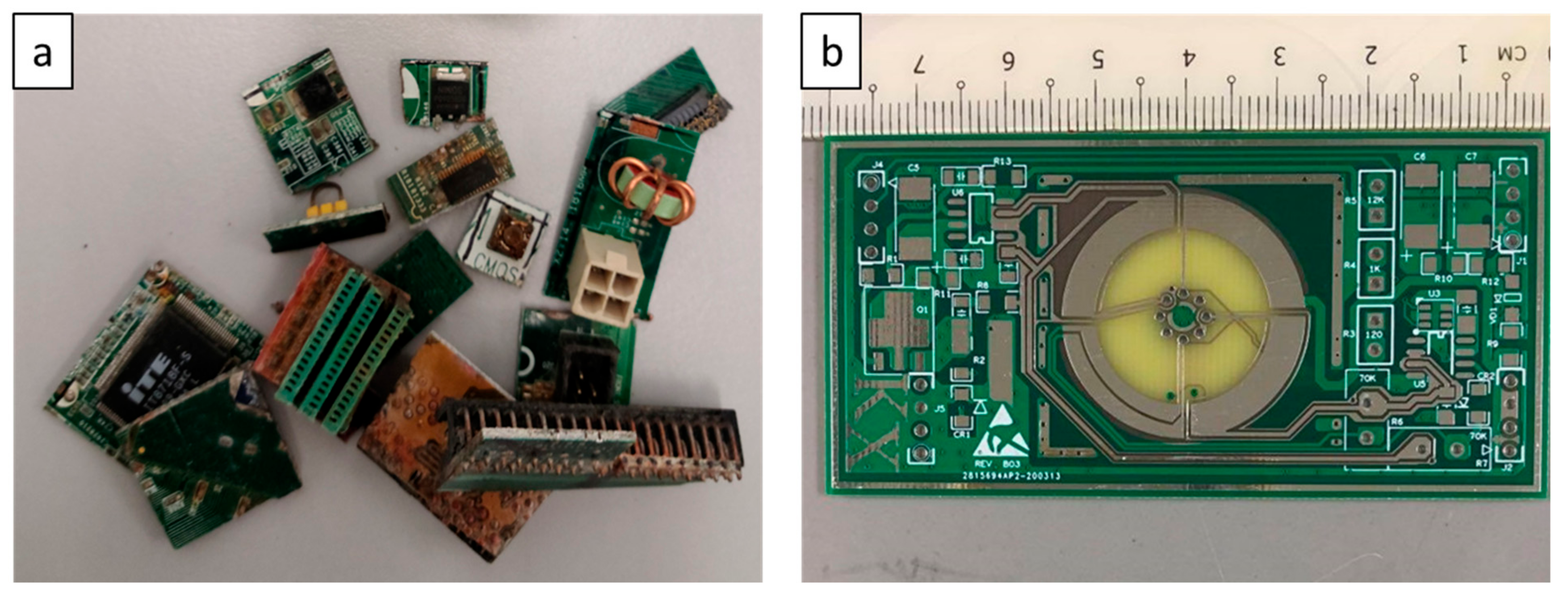
Figure 1.
(a) Populated PCBs (b) unpopulated PCBs.

Figure 4.
Resultant solid residue in coarse particle based pyrolysis: (a) unseparated pyrolytic solid residue—Reused from [57] with permission from Journal of Analytical and Applied Pyrolysis, (b) separated pyrolytic solid residue—Reused from [72] with permission from Science of the Total Environment.

Figure 5.
Non-liberated PCB particles after mechanical pre-treatment. Reused from [53] with permission from Waste Management.
Figure 5.
Non-liberated PCB particles after mechanical pre-treatment. Reused from [53] with permission from Waste Management.

Figure 6.
Change in cracking mode of PCBs after heat-treatment. Reproduced from [53] with permission from Waste Management.
Figure 6.
Change in cracking mode of PCBs after heat-treatment. Reproduced from [53] with permission from Waste Management.

Figure 7.
Coarse PCB pieces (a) before the removal of solder mask, and (b) after the removal of solder mask (conditions: 3M NaOH, 70 °C, 2 h, 1 cm × 1 cm PCB pieces, S/L ratio 1:5).
Figure 7.
Coarse PCB pieces (a) before the removal of solder mask, and (b) after the removal of solder mask (conditions: 3M NaOH, 70 °C, 2 h, 1 cm × 1 cm PCB pieces, S/L ratio 1:5).

Figure 8.
Conventional PCB pre-treatment flowsheet for hydrometallurgical e-waste recycling processes.
Figure 8.
Conventional PCB pre-treatment flowsheet for hydrometallurgical e-waste recycling processes.

Figure 9.
Proposed potential flowsheets for coarse PCB pieces: (a) chemical and mechanical pre-treatment (b) pyrolysis and mechanical pre-treatment and (c) thermal shock and mechanical pre-treatment processes.
Figure 9.
Proposed potential flowsheets for coarse PCB pieces: (a) chemical and mechanical pre-treatment (b) pyrolysis and mechanical pre-treatment and (c) thermal shock and mechanical pre-treatment processes.

Table 2.
Energy consumption for different HVEP fragmentation stages [89].
Table 2.
Energy consumption for different HVEP fragmentation stages [89].
| HVEP Fragmentation Stages | Fragmentation Outcomes | Estimated Average Energy Consumption (kWh/t) |
|---|---|---|
| 1 | Removal of ECs | 132 |
| 2 | PCBs structural delamination | 877 |
| 3 | Size reduction of PCBs | 1485 |
Table 3.
Individual qualitative comparison of different coarse PCB pieces pre-treatment methods (Note: quantitative comparison is not performed due to limited data).
Table 3.
Individual qualitative comparison of different coarse PCB pieces pre-treatment methods (Note: quantitative comparison is not performed due to limited data).
| Pre-Treatment Method | Extent of Delamination | Energy Consumption | Environmental Impacts (e.g., Dioxins, Dust) |
|---|---|---|---|
| Thermal shock | Medium | Medium | Medium |
| Pyrolysis | Medium-High | High | High—controls are required |
| Microwave induced pyrolysis | High | High | High—controls are required |
| Mechanical without prior pre-treatment | Low | High | Medium-High |
| Mechanical with prior pre-treatment | Medium | Low | Low-Medium |
| Chemical—solder mask removal | Very Low | Low | Low |
| Chemical—organic swelling | High | Low | Low |
| Chemical—microwave induced organic swelling | Very High | High | Low |
| HVEP comminution | High | Very high | Low |
Publisher’s Note: MDPI stays neutral with regard to jurisdictional claims in published maps and institutional affiliations. |
© 2021 by the authors. Licensee MDPI, Basel, Switzerland. This article is an open access article distributed under the terms and conditions of the Creative Commons Attribution (CC BY) license (https://creativecommons.org/licenses/by/4.0/).
Share and Cite
MDPI and ACS Style
Kang, K.D.; Ilankoon, I.M.S.K.; Dushyantha, N.; Chong, M.N. Assessment of Pre-Treatment Techniques for Coarse Printed Circuit Boards (PCBs) Recycling. Minerals 2021, 11, 1134. https://0-doi-org.brum.beds.ac.uk/10.3390/min11101134
AMA Style
Kang KD, Ilankoon IMSK, Dushyantha N, Chong MN. Assessment of Pre-Treatment Techniques for Coarse Printed Circuit Boards (PCBs) Recycling. Minerals. 2021; 11(10):1134. https://0-doi-org.brum.beds.ac.uk/10.3390/min11101134
Chicago/Turabian StyleKang, Kai Dean, I. M. Saman K. Ilankoon, Nimila Dushyantha, and Meng Nan Chong. 2021. "Assessment of Pre-Treatment Techniques for Coarse Printed Circuit Boards (PCBs) Recycling" Minerals 11, no. 10: 1134. https://0-doi-org.brum.beds.ac.uk/10.3390/min11101134
Note that from the first issue of 2016, this journal uses article numbers instead of page numbers. See further details here.