
Molecular Insight into the Deformation of Single Crystal Copper Loaded by High-Speed Shock Wave

1
School of Mathematics and Physics, China University of Geosciences (Wuhan), Wuhan 430074, China
2
State Key Laboratory of Geological Process and Mineral Resources, Faculty of Earth Sciences, China University of Geosciences (Wuhan), Wuhan 430074, China
*
Author to whom correspondence should be addressed.
Metals 2021, 11(3), 446; https://0-doi-org.brum.beds.ac.uk/10.3390/met11030446
Submission received: 3 February 2021
/
Revised: 26 February 2021
/
Accepted: 4 March 2021
/
Published: 8 March 2021
(This article belongs to the Special Issue Shock-Wave Loading of Metallic Materials)
Abstract
:Molecular dynamics simulations were performed to study the evolution of single crystal copper with and without a nanovoid (located at the middle of crystal with a diameter of ~2.9 nm) when loaded with shock waves of different velocities. The simulation results show that the average particle velocity of single crystal copper linearly relates to the velocity of the loaded shock wave for both the systems (crystal with and without a nanovoid). When loaded by the shock wave, the equilibrated temperature and pressure of the system with a nanovoid are found to be slightly larger than those of the system without the nanovoid, while the volume of the system with the nanovoid is found to be lower than that of the void-free system. The single crystal copper undergoes a phase transition from face-centered cubic (FCC) to hexagonal-close packed (HCP) and a dislocation structure forms around the nanovoid. The existence of a nanovoid can induce the rearrangement and deformation of the crystalline structure and eventually lead to the plastic deformation of the system. This work provides molecular-level insight into the effect of nanovoids on the shock plasticity of metals, which can aid in the ultimate application of the control of material structure damage in shock-wave propagation.
1. Introduction
A material may undergo structural damage when a strong shock wave propagates through a material because real materials may contain a large number of defects, such as vacancies [1,2,3], dislocations [4,5,6,7,8,9], grain boundaries [10,11,12,13], and micropores [14]. Shock-induced structural damage is a disadvantage in shock compression science and technology. Therefore, it is essential to understand the main influential factors and the kinetic behavior of the structural damage, to control and decrease the unexpected damage. Nevertheless, structural damage in materials is a complex process involving material mechanics [15,16], kinetics [17], thermodynamics [18], etc. The accumulation of plastic damage induced by the plastic deformation of materials is one of the primary causes of ductile material fracture [19,20,21,22]. Significant amounts of research have focused on this deformation process. Studies of the effect of defects on the deformation of face-centered cubic (FCC) metal with shock loading have become an important subject both in theoretical and experimental research [13,23,24]. However, the analysis of the plastic deformation of materials is limited by the low temporal and spatial resolution of the experimental setups.
Molecular dynamics (MD) simulations can show the clear evolution of the system and the velocity vector inside the material at different times on the femtosecond time scale and nanometer space scale. Hence, the deformation process inside the material and the dynamic evolution of microscopic defects under compression and tensile stresses can be clearly analyzed [25,26,27]. In recent years, MD simulations combined with other numerical computation methods have been used to study the emergence and the development of single defects under shock-loading conditions [5,28,29,30,31,32,33]. Bringa et al. [34] carried out nonequilibrium molecular dynamics method (NEMD) to simulate a nanometer single crystal copper loaded by a plane shock wave. The results show that the single crystal copper begins to undergo plastic deformation and melting between 200 and 220 GPa when the particle velocity is 0.75 km/s. Lin et al. [35] utilized an MD simulation with embedded atomic potential (EAM) to study the influence of crystal orientation ([100] [110] [111]) on the dynamic response of single crystal copper. The simulation results characterized the defective Cu system in terms of Hugoniot behavior, local tissue evolution, and fracture strength during the shock wave propagation. Neogi and Mitra [36] studied the shock response of a nanovoid closed/open-cell copper material using NEMD simulations and found that the Hugoniot elastic limit (HEL) point decreases with increasing porosity. Typically, the HEL for open-cell pore structures is lower than that for close-cell pore structures, and the rate of void collapse is faster for the latter. Xiong et al. [37] used MD simulation to reveal that plastic deformation occurs under shock compression that is lower than the HEL for copper due to the existence of cylindrical voids. In addition to that, Xiong et al. [38,39,40] studied the mechanical behavior of materials under ultrafast nonequilibrium deformation. Neogi et al. [41] combined MD simulations with ab initio calculations to conduct impact simulation for single crystal copper with a model of 100 holes and confirmed that the FCC to body-centered tetragonal phase transition would occur in the orientation of [100]. Cao et al. [42] studied the formation of a single crystal double-wave structure with the shock wave simulated by MD simulation and analyzed the dislocation structure caused by shock compression along the orientation of [001] and [221]. Patil et al. [43] investigated the shockwave response of graphene aerogels of a wide range of densities from 149 to 679 kg/m3 using MD simulations. In addition, he [44] also used MD simulations to study high-velocity shock compression of a wide range of silica aerogel densities from 209 to 847 kg/m3 according to the reverse ballistic approach. The reverse ballistic approach can consider a wide range of shock velocities.
There are a few studies on the shock wave loading of single crystal copper using the multi-scale shock technique (MSST) in MD simulations. However, these studies paid little attention to the effects of nanovoid on thermodynamic parameters. Instead of simulating the shock wave in a large computing unit with many atoms, the multi-scale shock wave was passed through the Lagrangian point of the shock waves, which allowed the shock wave to be simulated with fewer atoms and lower computational costs [45]. The combination of MSST and MD simulation is based on the Navier–Stokes equation [46,47,48,49]. Compared with other MD methods, this method not only ensures the accuracy of the results, but also significantly reduces the required material size and the calculation time [48].
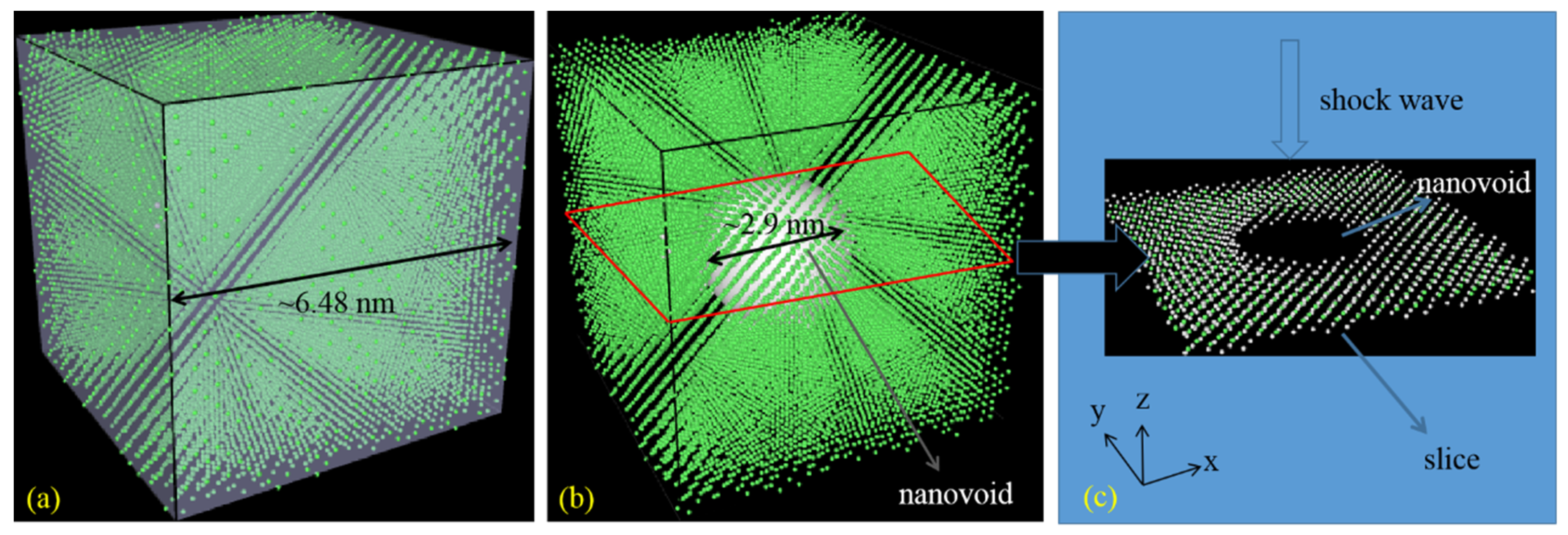
In this paper, MD simulations with the MSST method are performed to study two different single crystal copper systems loaded by a compressive shock wave with different velocities. A perfect single crystal copper system (named voids-free system) and a single crystal copper system with a large nanovoid (located at the center of the copper crystal and named nanovoid-containing system) are studied here. Their X, Y, and Z axes are along the [100], [010], and [001] directions, respectively. The schematics of the two systems are shown in Figure 1. The model dimensions are 6.48 nm × 6.48 nm × 6.48 nm. The MD model of single-crystal copper with a spherical nanovoid is created as shown in Figure 1b. The diameter of the spherical nanovoid is about 2.9 nm. Thermodynamic parameters (such as temperature, pressure, and volume of the two systems) and statistical mechanical parameters (radial distribution function (RDF) and mean squared displacement (MSD)) are calculated to characterize the properties of the two systems. Section 1 briefly introduces the background and significance of the study. Section 2 describes the model and simulation details. Section 3 describes the results and discussions, followed by the main conclusions (Section 4).
2. Simulation Methodology
The MSST method can simulate a shockwave loaded atomic system, in which the pressure and energy changes follow the continuum theory which describes the states before and after the shockwave structure [50].
where v is the shock wave velocity and ρ is the system density. The parameters with subscript 0 correspond to the initial state, and the parameters without a subscript indicate the state loaded by the shock wave. Equation (1) is the Rayleigh relation, which is used to constrain the system pressure. E and V represent the system energy and volume, respectively. Equation (2) is the shock Hugoniot relation, which is used to represent the energy state before and behind the wave array during the shock wave loading. The above equations describe the thermodynamic pathways of the initial and final states of the shock wave when the material is loaded by a shock wave at a steady velocity. To ensure the stability of the system, the wave velocity of the shock wave should be subject to two limiting conditions when it is propagating in nanocrystal copper [45]. According to these two limiting conditions, the velocity of the shock wave should be limited to 4–9 km/s.
The interaction potential between atoms is described by the potential function, which is of vital importance for handling motion equations in MD simulations. In this paper, we selected the EAM potential function [51,52], which is defined as
where Equation (3) represents the total energy of an atom i in a single atomic system. Equation (4) represents the electron cloud density, where is the total potential energy, is the pair potential, is an embedded function that can be a tightly bound potential approximation of the sum of the squares of the hopping integral, is potential of electron cloud density, and is the total density of the electron cloud.
The unit cell of single crystal copper has FCC structure and the lattice parameter a = 3.61 Å. The constructed voids-free system consists of 18 × 18 × 18 supercells. Atoms within a sphere r = 4a are dug out from the center of the voids-free system to make the nanovoid-containing system. Both systems adopt the three-dimensional periodic boundary condition. To obtain reliable and repeatable results from the MD simulations both systems are well equilibrated by a 20 ps NVT simulation under 300 K temperature condition. The integral step is 1 fs. Combined with MSST, the shock compression is carried out along the [001] crystal orientation (z direction). The shock compression process lasts for a total of 20 ps with the shock wave velocities ranging from 4–9 km/s. Both systems reach an equilibrium state after the shock wave is loaded. All simulations were performed using the large-scale atomic/molecular massively parallel simulator (LAMMPS) [53], which was developed by Sandia National Laboratory in the United States for computational and simulation work related to MD. In general, LAMMPS can be coded to solve the MD simulation of metals [54,55]. To identify the structural defect and local structure types during the deformation process, all MD snapshots are visualized using the open visualization tool (OVITO) [56].
3. Results and Discussion
3.1. Particle Velocities of Copper Loaded by Shock Waves
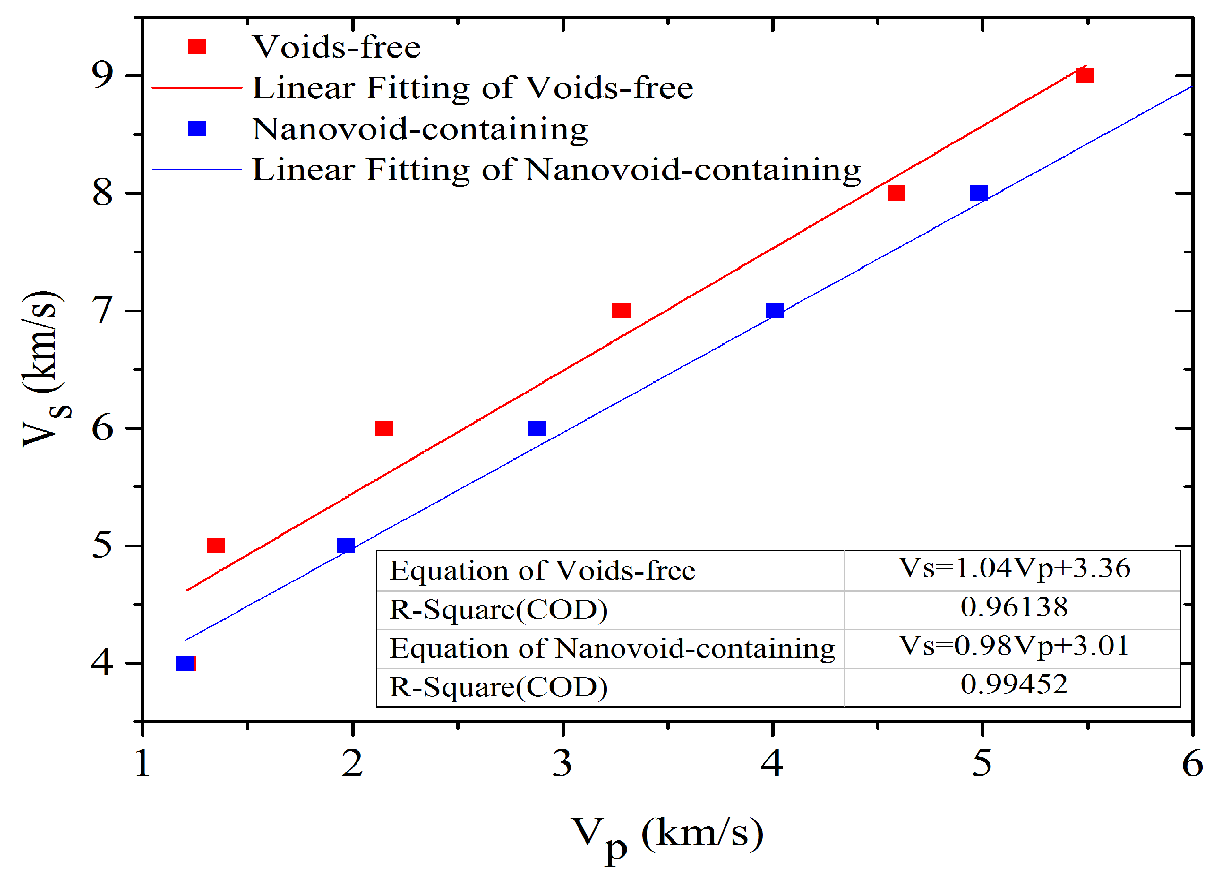
In material systems, the shock wave velocity (Vs) and the particle velocity (Vp) are linearly related. Here, both the shock-wave-loaded single crystal copper systems (voids-free system and nanovoid-containing system) satisfy the linear relation, Vs = C + SVp, where C is a constant and represents the sound velocity of the system without loading, and S is the slope factor [29]. Figure 2 presents both the corresponding velocities (Vs and Vp) of the two systems and has been fitted by linear functions. The results show that the two velocities depend linearly on each other and are similar to previously reported experimental results [34]. Therefore, MD simulations with MSST can reliably reproduce the response processes of single crystal copper loaded by shock wave. According to the fitting lines, the sound velocity of a perfect copper crystal is about 0.35 km/s faster than that of the copper system with a nanovoid. It should be noticed that the Vp for the two systems is almost the same when the system is loaded by a 4 km/s shock wave. This is because 4 km/s just meets the minimum shock wave speed required by the MSST method.
3.2. Time Evolution of Thermodynamic Parameters
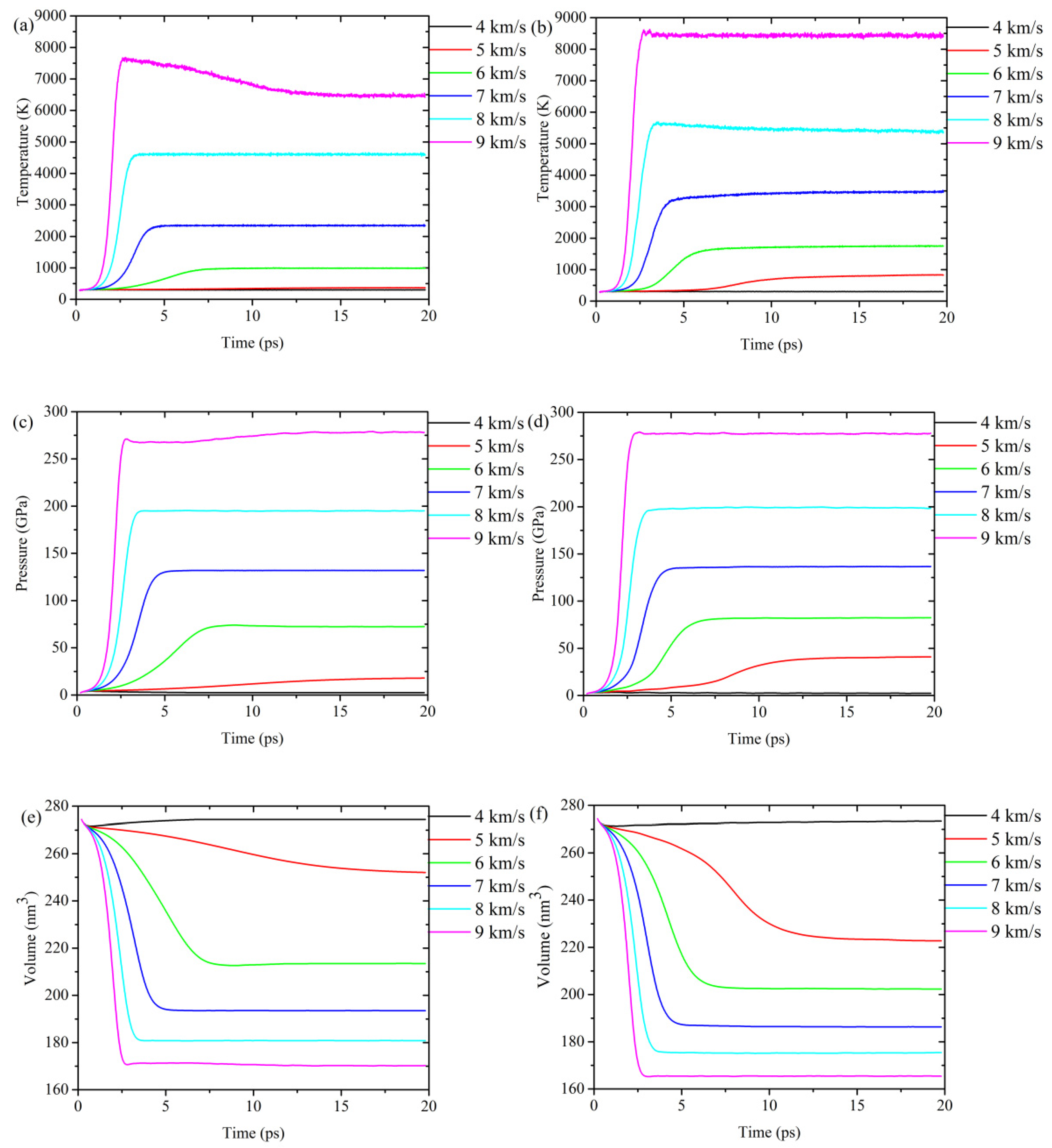
Generally, thermodynamic parameters (such as temperature, pressure, and volume) are utilized to describe the shock compression process of material systems before and after the shock wave array in MSST, and this method restricts the atomic system to the thermodynamic state behind the macroscopic shock wave. The time variations of the temperature, pressure, and volume profiles of the voids-free system and the nanovoid-containing system loaded by shock waves with different velocities (4–9 km/s) are shown in Figure 3. Under the same conditions, the induction time of the nanovoid-containing system from the elastic to the plastic stage is shorter than that of the voids-free system. With the increase in shock wave velocity, the induction time from the elastic to the plastic stage is shortened for both the voids-free system and the nanovoid-containing system.
The change in the temperature of the voids-free system and the nanovoid-containing system over time are shown in Figure 3a,b, respectively. The equilibrium temperature increases sharply as the wave velocity increases in both the voids-free system and the nanovoid-containing system. However, the equilibrium temperature in the nanovoid-containing system is slightly higher than in the voids-free system at the same shock wave velocity because of the nanovoid. Similarly, the change in the pressure of the voids-free system and the nanovoid-containing system over time is shown in Figure 3c,d, respectively. The equilibrium pressure of the nanovoid-containing system is slightly higher than that of the voids-free system. We find that the inflection point of pressure occurs at the same time as the inflection point of temperature. The change in the volume of the voids-free system and the nanovoid-containing system over time is shown in Figure 3e,f, respectively. Figure 3e,f shows that the volume of the two systems are rapidly compressed, and the volume inflection point also occurs at almost the same time as the temperature and pressure inflection points. In addition, we can see from these six figures that 5 km/s is a special velocity. When the velocity of the shock wave is 5 km/s, the two systems have obvious differences, and the volume of the nanovoid-containing system is more significantly compressed. Therefore, in this paper the structural change of the nanovoid-containing system at 5 km/s will be discussed in detail in Section 3.3.
When the loaded shock wave velocity is 4 km/s, the three thermodynamic parameters of the two systems are basically unchanged. This is because the system is basically in the state of elastic deformation during the shock wave loading. Hence, the effect of the loading is less. In contrast, when the loaded shock wave velocity is greater than 5 km/s, the temperature profiles of the two systems rise sharply and reach the peak rapidly. The higher the shock wave velocity, the faster the temperature rising rate, and the shorter the time to reach the peak value. The rapid temperature rise of the systems causes the internal transformation from elasticity to plasticity within the materials. When the shock wave velocity is 9 km/s, the temperature of the voids-free system reaches the peak value (T = 7665 K) at 2.64 ps, and then the temperature drops slowly to an equilibrium state (T~6500 K at 12 ps). The temperature of the nanovoid-containing system reaches the peak value (T = 8421 K at 2.6 ps), and the temperature remains mostly constant with little fluctuation. Under this condition, the shock wave velocity is so large that the lattices of the voids-free system directly translate to a disordered state without the elastic deformation process.
For a shock compression system with higher shock wave velocity, the equilibrium temperature and pressure are both higher than that with a lower shock wave velocity. With the increase in shock wave velocity, the transition induction time of the system from the elastic to the plastic stage becomes significantly shorter, and the transition induction time is shown in Table 1. For the nanovoid-containing system, the induction time from the elastic stage to the plastic stage is shorter than that of the voids-free system (as shown in Table 1). The final temperature and pressure of the nanovoid-containing system are slightly higher than that of the voids-free system, and the volume is slightly smaller than that of the voids-free system. Hence, the deformation of single crystal copper is influenced by the nanovoid within the system. This finding may be attributed to the early formation of dislocations around the nanovoid, which induce the shock wave to compress the system more rapidly, leading to a large difference in thermodynamic properties.
3.3. Phase Transition and Dislocation Pathway
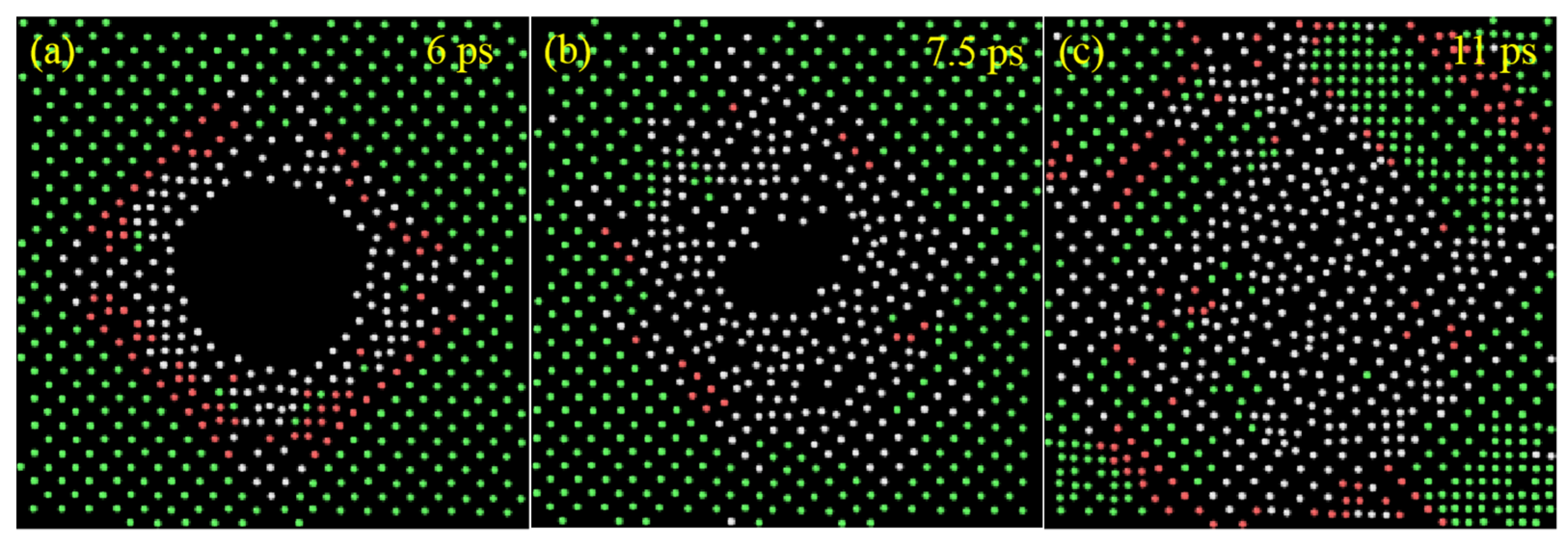
The common neighbor analysis (CNA) described by Faken and Jónsson are employed to identify the structural defect and local structure types during the deformation process [57]. In this study, we found that both the voids-free system and the nanovoid-containing system undergo FCC-HCP phase transition, and the phase transition rate of the voids-free system is approximately half that of the nanovoid-containing system. Figure 4 shows the phase transition process of the nanovoid-containing system when the shock wave velocity is 5 km/s in the xy plane. It clearly shows that atoms in the FCC structure (green atom) translate to the HCP structure (red atom) with time, and the number of disordered atoms (white atom) increases. Additionally, the disordered atoms first appear around the nanovoid. The disordered atoms are surrounded by copper atoms with the HCP structure, and the outer layer is occupied by copper atoms with the FCC structure. This phase transition happens because the Schmid factor changes when a shock wave is reflected from the free surface of the void [37]. With the shock wave loading, disordered atoms appear in the nanovoid space and their presence begins to increase from the center to the edge in the nanovoid-containing system. When the shock wave velocity is larger than 7 km/s, we do not observe this gradual phenomenon, and with the increase of the shock wave velocity, the ratio of copper atoms with HCP structure becomes smaller. When the shock wave velocity is 9 km/s, the system particles will change from the FCC structure to a disorderly state in a very short amount of time, skipping the intermediate transition from the elastic stage to the plastic stage.
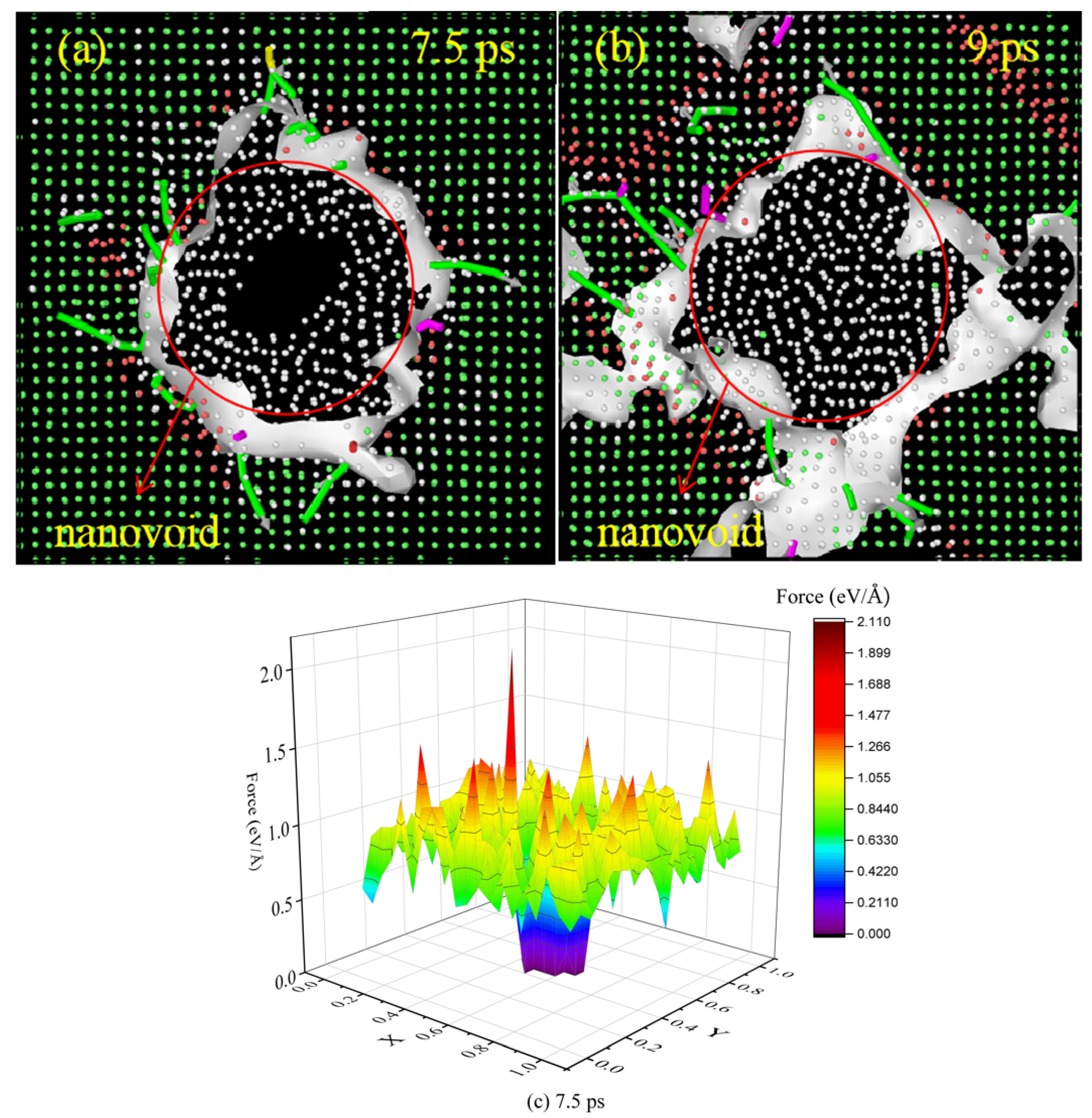
The FCC to HCP phase transition takes place around the nanovoid, and eventually the disordered atoms occupy the nanovoid. The phase transition from the FCC to the HCP structure occurs as the shock waves can induce the nanovoid-containing system producing a dislocation structure. In a single crystal copper system, the shortest perfect dislocation slip vector is (a/2)[110]. However, the slip barrier of (a/2)[110] is much higher than that of (a/6)[112]. Therefore, in the FCC structure, perfect dislocations will generally be decomposed into partial dislocations and a layer of stacking fault will occur between the partial dislocations. The HCP structure will appear around the partial dislocation region. Figure 5 shows that different dislocations are formed around the nanovoid when the shock wave velocity is 5 km/s. The dislocation theory provides the basic framework for the plastic deformation of materials. Thus, in order to understand the plastic deformation around the nanovoid, it is necessary to know the formation and growth of the dislocation structure in this area. The observed movements of different types of dislocations from 7.5 ps to 9 ps are shown in Figure 5a,b. The green color represents the Shockley partial dislocation in the 1/6[112] orientation, the purple color represents the stair-rod dislocation in the 1/6[110] orientation, the yellow color represents the Hirth dislocation in the 1/3[110] orientation, and the gray arrows on the dislocation represent the Burgers vector. Moreover, the white areas represent the defect mesh. The location where the dislocation occurs corresponds to the peak force exerted on the atom at that location and the dislocation grows from the center to the edge. It is shown that most of the dislocations are Shockley partial dislocations in the (a/6)[112] orientation, and the direction of the Burgers vector is from the center to the edge. This indicates that the dislocation structure emerges from around the nanovoid and grows toward the edge of the simulation system. Dislocation theory considers that the driving force of dislocation motion is the decomposed shear stress on the slip system. To further understand the dislocation motion process, the atomic force along the [001] crystal orientation is calculated in this paper and we find that the peak force in Figure 5c corresponds to the dislocation structure in Figure 5a. It is worth mentioning that FCC copper may undergo deformation twinning along the {111} planes. Twinning means that one part of the crystal slides relative to the other, and the energy required is generally higher than that of dislocation propagation. The deformation twins of single crystal materials have strong orientation dependence. Due to the orientation dependence of plastic deformation, the active slip systems in different grains are obviously different, which will lead to grain boundary migration. When a series of adjacent {111} planes slip continuously with 1/6[112] partial dislocations, twins begin to form and expand.
3.4. RDF and MSD
In MD simulations, the RDF is often used to analyze the crystal structure. It describes the probability of finding another particle within a radius of r~(r + dr) with one particle in the system as the center. The ratio of the atomic number density of each shell to the average density is the RDF, which is defined as
where r is the radius from the central atom, δr is the thickness of the shell, n(r) is the number of particles in the shell, and ρ is the density in the ideal crystal.
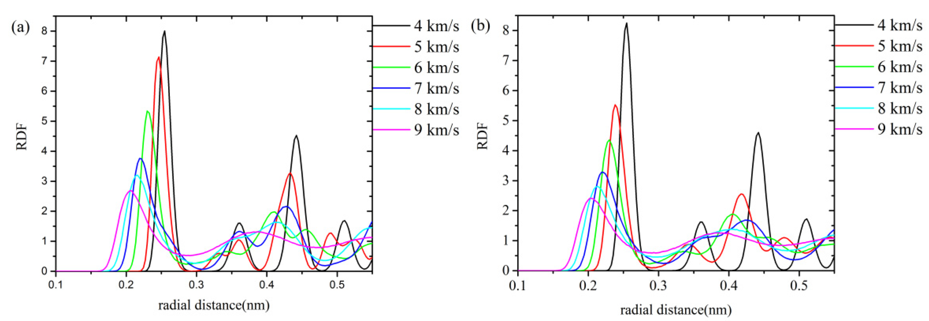
In a crystal, atoms are arranged periodically. According to the physical meaning of the RDF, each layer of atoms has a peak value, while between the atom shells, the probability of atomic occurrence is 0, and the RDF gradually approaches 1 at infinity. In Figure 6a,b, when the shock wave velocity is 4 km/s, the peak value of RDF drops to 0 rapidly after reaching its maximum value, followed by regular peaks and troughs, indicating that copper is still in the crystal state at this time. When the shock wave velocity increases to 6 km/s, the RDF also exhibits a first sharp peak and then drops to the first trough. However, in this case the trough value is not equal to 0, which indicates that copper has begun to transform from crystalline to amorphous form. The higher the shock wave velocity, the closer the value of the first trough is to 1, indicating that the atom movement is intensified and affected by the shock wave. The RDF of ordered crystals has long range peaks. The RDF of amorphous crystals only has short range peaks. Figure 6a shows the RDF of the voids-free system loaded by shock waves of different velocities. The first peak of RDF moves to the left and decreases as the shock wave velocity increases for both the voids-free system and the nanovoid-containing system. The peak value of RDF for the nanovoid-containing system is slightly smaller than that for the voids-free system at the same shock wave velocities. As the wave velocity of the shock wave increases, the peak value decreases gradually and the peak width increases, indicating the transition of the single crystal copper system into the amorphous form. When the shock wave velocity is greater than 5 km/s, the first peak value of RDF for the nanovoid-containing system is obviously lower than that of the voids-free crystal, which indicates that the existence of the nanovoid will accelerate the system’s transition to the amorphous form. This influence is most obvious when the shock wave velocity is approximately 5 km/s.
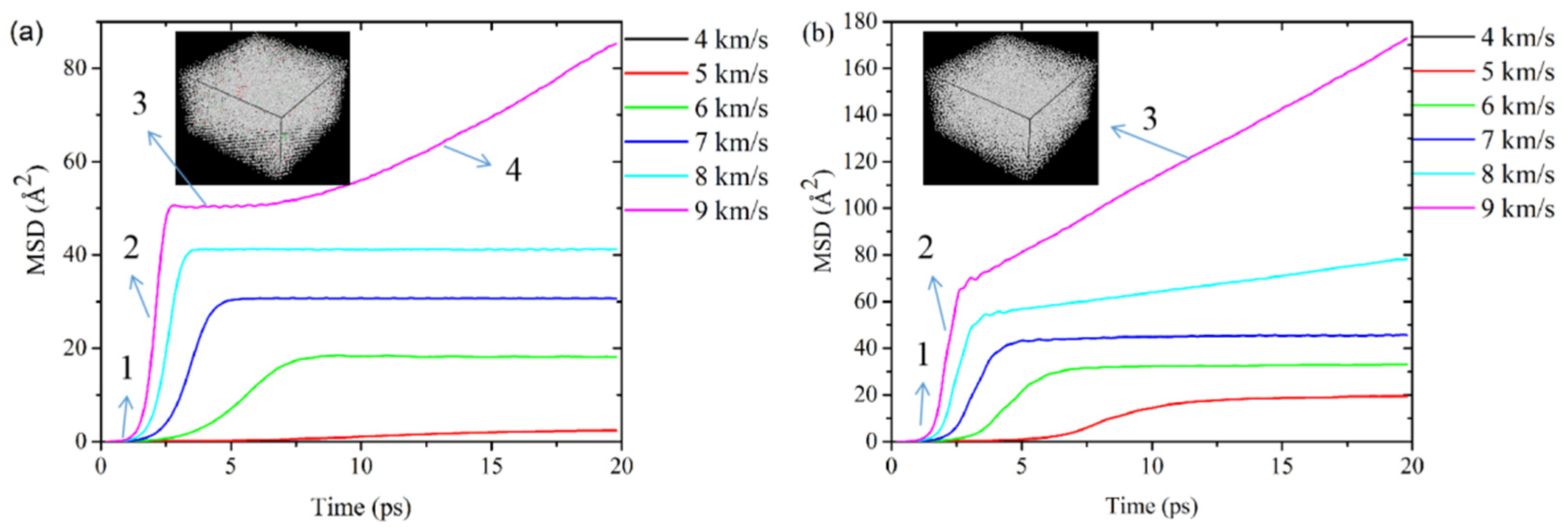
Further, we used MSD to describe the diffusion behavior of particles in the system under the action of the shock wave. In the single crystal copper system, the mean value of the square of atomic displacement is the MSD, which is defined as [58]
where r(t) represents the position of the particles at time t, and N represents the number of particles. According to Einstein’s law of diffusion,
where D is the diffusion coefficient, the MSD is proportional to time, and the ratio is 6D.
Figure 7a,b shows the MSD for the copper atom of the voids-free system and nanovoid-containing system loaded with shock waves of different velocities. When the wave velocity of the shock wave is less than 5 km/s, the MSD is close to 0. This means that the system is still in a crystal state and the particles in the system have almost no free diffusion.
When the shock wave velocity is greater than 5 km/s, the MSD grows approximately linearly at first, according to Einstein’s diffusion law. The diffusion coefficient of the voids-free system can be calculated and is shown in Table 2. It shows that the diffusion coefficient increases with the increase in the shock wave velocity. At this stage, the system rapidly diffuses within 0–5 ps, and the system changes dramatically from the crystal state to the amorphous state (5 km/s velocity loading simulation as an example). After 5 ps, the MSD remains almost constant, at which point the free diffusion of particles in the system ends. This is because most of the atoms in the system are still constrained in the crystal lattice, although the crystal structure has been partially deformed.
It should be noted that the MSD (a) reveals four distinct regions when the loaded shock wave velocity is 9 km/s for the voids-free system: a slow rise from 0–1 ps, a region with a nearly constant slope (1–3 ps), the MSD gradually reaches a plateau, and then finally continues to spread. In the first stage, the system shrinks rapidly by a compressive shock wave passing over. The copper atoms are compressed and a phase transition is performed under the large loading in the second stage. In the third stage, few copper atoms in the system remain in the crystal structure. In the final stage, the lattice structure is destroyed and all the atoms move freely. There will be a region of further diffusion when the shock wave velocity is 9 km/s. The diffusion coefficient is about 3.2 × 10⁻¹⁰ m2/s for solids and 1.9 × 10⁻⁸ m2/s for melts which is 2 orders of magnitude higher. This result is consistent with the results of He [24] and An [59]. An et al. [59] roughly identified partial melting regimes as Vp = 3.3–3.5 km/s, and this paper identifies partial melting at 3.7 km/s in terms of Vp. In contrast, the MSD (b) for the nanovoid-containing system has no plateau stages after 2.5 ps. This is because the presence of the nanovoid could accelerate the speed of phase transition. Therefore, the MSD does not exhibit the plateau stage in this case.
3.5. Time Evolution of System Stress
The comprehensive stress of materials is the reflection of internal “tractions” and can describe the structure strength and the failure of them under external loading. Therefore, the investigation of the comprehensive stress of copper (with and without a void (defect)) is one of the effective approaches in understanding the deformation and damage mechanism of copper under shock wave loading. Here, we calculated the time variation of the principal stress () along the shock wave direction), hydrostatic pressure (), shear stress (), and the Von-Mises stress () for the both copper systems, and all the definition are shown in the following equations.
where the , , and correspond to the principal stresses in the x, y, and z direction, respectively.
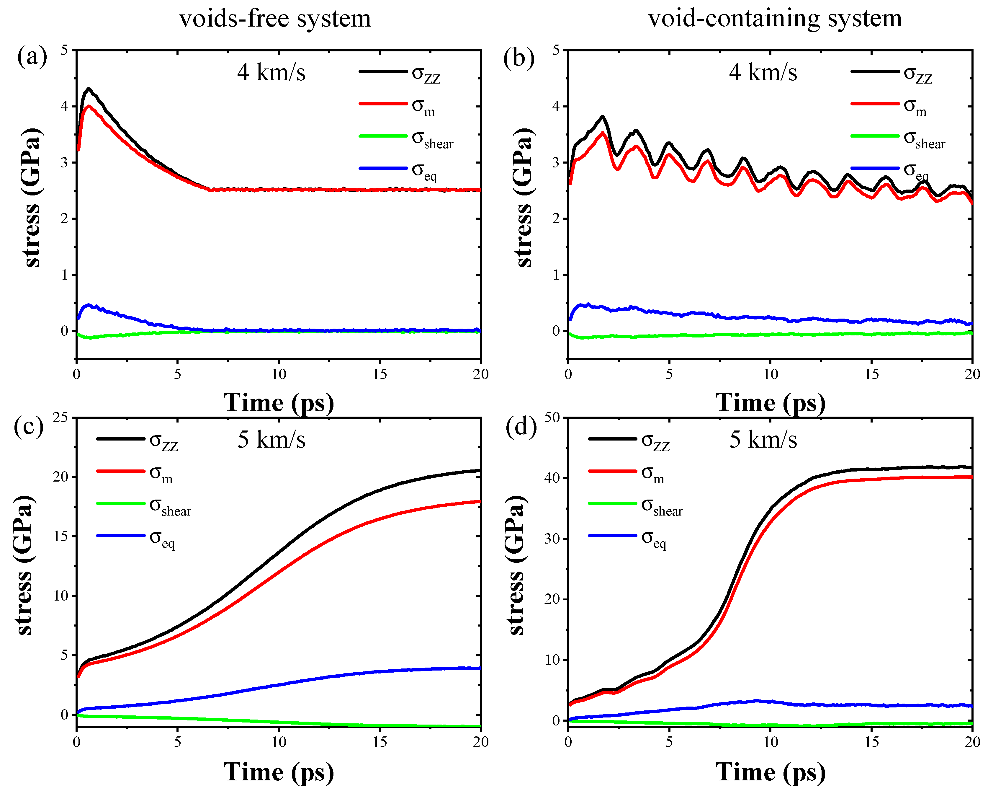
The stress curves for the two systems under two different shock waves velocities (4 km/s and 5 km/s) are shown in Figure 8. As discussed above, the states of the copper loaded by the shock waves with two different velocities are corresponding to the elastic and plastic deformation respectively. Based on the Figure 8, the time variation trend of the and the is almost the same, and the former is slightly less than the later under the same conditions and simulation time, that means the stress value in the shock direction is greater than that in the other two directions. In contrast, the value of shear stress and the Von-Mises stress for the two systems are much less than that of the above two stresses. Results also show obviously that the variation of is quite different loaded by shock waves with different velocities. When the velocity of shock wave is equal to 4 km/s, the of the voids-free system first increases linearly up to the maximum value (4.2 GPa) at 0.6 ps, and then begins to decrease and finally reaches to the equilibrium value (2.5 GPa) at 6.5 ps (Figure 8a). For the void-containing system, the fluctuates and decreases slowly, that means this system is still in yield phase until the MD simulation is completed (Figure 8b). When the velocity of shock wave is up to 5 km/s, the for the both systems increases rapidly to several tens of GPa first, the difference is that the strength of the void-containing system is much larger than that of voids-free system, meanwhile, the stress for the void-containing system can reach to an equilibrium value (42 GPa) during the MD simulations, while the stress for the other system is not, which also indicates that the void within the material system can accelerate the deformation and damage process of material. This result is similar to the experimental result of Patil et al. [60]. The results of their study show that the shock wave-forming process is a feasible technique for mass production of stacked metallic sheets as well as fabricating a hierarchical composite structure, which provides higher formability and smooth thickness distribution compared to a single material.
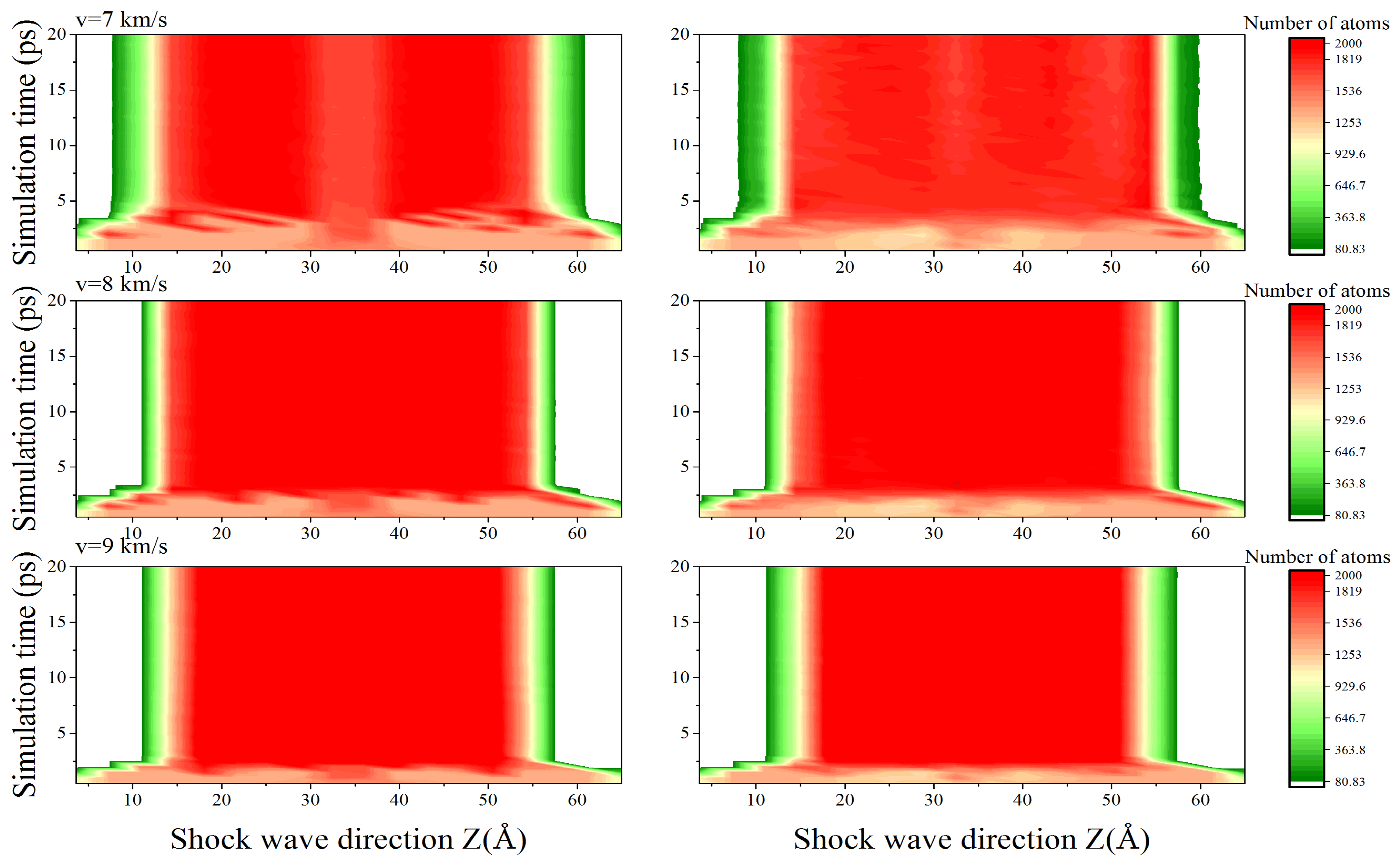
Figure 9 illustrates how the number of atoms in the fixed-volume bin varies throughout the shock wave simulations. The number of copper atoms in a fixed-volume bin is referred to as the bin-density. The temporal-spatial distribution plots show that the bin-density was constant throughout the shock direction of the simulation systems before the shock compression.
4. Conclusions
In summary, we have studied the dynamic evolution of a single crystal copper system and a nanovoid-containing system under shock wave loading along [001] crystal orientation by employing MD simulations in conjunction with MSST. The results show that there is a linear relationship between the velocity of the shock wave and the particle velocity, which is consistent with the experimental results. The phase transitions and dislocations around the nanovoid evolving with time are studied in detail. Under the influence of shock wave loading, the existence of the nanovoid induces a dislocation structure. The dislocation structure grows from the center to the edge of the system. A phase transition from FCC to HCP structure could occur in the dislocation region. As a result, the atomic motion of the system increases, which is manifested in the rise of temperature and pressure in the system at the macro level. Similarly, MSD and RDF have been used to prove that the existence of the nanovoid will increase the temperature and pressure of the system, and an increase in shock wave speed has the same effect. These results can provide a reference for the influence of the changes in metal microstructures on the macroscopic thermodynamic state. This work provides molecular-level insight into the effect of nanovoids on the shock plasticity of metals, which can aid in the ultimate application of the control of material structure damage in shock wave propagation. The reverse-ballistic approach will be used in future studies. In addition, the combination with experiments should be considered in future work.
Author Contributions
Literature search, C.Z.; figures, C.Z. and B.F.; data collection, C.Z.; writing, C.Z.; data analysis, B.F.; formal analysis, J.M.; survey, J.C. and Y.Z.; supervision, T.L.; review and revision, T.L. All authors have read and agreed to the published version of the manuscript.
Funding
This research was funded by the project of the National Natural Science Foundation of China (Grant No. 41573016).
Institutional Review Board Statement
Not applicable.
Informed Consent Statement
Not applicable.
Data Availability Statement
Not applicable.
Conflicts of Interest
The authors declare no conflict of interest.
References
- Li, M.; Luo, Y.; Hu, X.; Han, Z.; Liu, X.; Cui, J. Co-regulation of the copper vacancy concentration and point defects leading to the enhanced thermoelectric performance of Cu 3 In 5 Te 9-based chalcogenides. RSC Adv. 2019, 9, 31747–31752. [Google Scholar] [CrossRef] [Green Version]
- Noell, P.J.; Sabisch, J.E.C.; Medlin, D.L.; Boyce, B.L. Nanoscale conditions for ductile void nucleation in copper: Vacancy condensation and the growth-limited microstructural state. Acta Mater. 2020, 184, 211–224. [Google Scholar] [CrossRef]
- Xue, L.; Ren, Y.; Hu, Z.; Hu, Y.; Li, Z. First principles study the influence of copper-vacancy on electronic, mechanical and thermal properties of CuGaTe2. Results Phys. 2019, 15, 102765. [Google Scholar] [CrossRef]
- Zhou, S.J.; Preston, D.L.; Lomdahl, P.S.; Beazley, D.M. Large-scale molecular dynamics simulations of dislocation intersection in copper. Science 1998, 279, 1525–1527. [Google Scholar] [CrossRef]
- Ahn, D.C.; Sofronis, P.; Kumar, M.; Belak, J.; Minich, R. Void growth by dislocation-loop emission. J. Appl. Phys. 2007, 101, 063514. [Google Scholar] [CrossRef]
- Jian, W.R.; Zhang, M.; Xu, S.; Beyerlein, I.J. Atomistic simulations of dynamics of an edge dislocation and its interaction with a void in copper: A comparative study. Model. Simul. Mater. Sci. Eng. 2020, 28, 045004. [Google Scholar] [CrossRef]
- Wei, D.A.; Zaiser, M.; Feng, Z.; Kang, G.; Fan, H.; Zhang, X. Effects of twin boundary orientation on plasticity of bicrystalline copper micropillars: A discrete dislocation dynamics simulation study. Acta Mater. 2019, 176, 289–296. [Google Scholar] [CrossRef]
- Xiong, J.; Wei, D.; Lu, S.; Kan, Q.; Kang, G.; Zhang, X. A three-dimensional discrete dislocation dynamics simulation on micropillar compression of single crystal copper with dislocation density gradient. Acta Metall. Sin. 2019, 55, 1477–1486. [Google Scholar] [CrossRef]
- Huang, S.H.; Chen, T.; Chen, Q.; Zhao, Z.D.; Xia, X.S. Verification of dislocation density and dynamic recrystallization in deformed pure copper. Strength Mater. 2020, 52, 1–8. [Google Scholar] [CrossRef]
- Koju, R.K.; Mishin, Y. Direct atomistic modeling of solute drag by moving grain boundaries. Acta Mater. 2020, 198, 111–120. [Google Scholar] [CrossRef]
- Zhang, J.; Zhang, H.; Ye, H.; Zheng, Y. Twin boundaries merely as intrinsically kinematic barriers for screw dislocation motion in fcc metals. Sci. Rep. 2016, 6, 22893. [Google Scholar] [CrossRef] [PubMed] [Green Version]
- Lu, K. Stabilizing nanostructures in metals using grain and twin boundary architectures. Nat. Rev. Mater. 2016, 1, 1–13. [Google Scholar] [CrossRef]
- Han, L.B.; An, Q.; Fu, R.S.; Zheng, L.; Luo, S.N. Local and bulk melting of Cu at grain boundaries. Phys. B 2010, 405, 748–753. [Google Scholar] [CrossRef] [Green Version]
- Zhang, L.; Wang, S. Correlation of materials property and performance with internal structures evolvement revealed by laboratory X-ray tomography. Materials 2018, 11, 1795. [Google Scholar] [CrossRef] [Green Version]
- Li, H.; Ding, Z.; Zhao, Y.; Zhao, R. Strength and its prediction models based on fracture mechanics of thin layers copper cladding steel wires under different amount of deformation. J. Mater. Sci. 2016, 27, 12499–12505. [Google Scholar] [CrossRef]
- Kondo, T.; Bi, X.C.; Hirakata, H.; Minoshima, K. Mechanics of fatigue crack initiation in submicron-thick freestanding copper films. Int. J. Fatigue 2016, 82, 12–28. [Google Scholar] [CrossRef]
- Li, P.; Li, Z. Theoretical Insights into the Thermodynamics and Kinetics of Graphene Growth on Copper Surfaces. J. Phys. Chem. C 2020, 124, 16233–16247. [Google Scholar] [CrossRef]
- Song, H.B.; Wang, X.; Patton, J.R.; Stansbury, J.W.; Bowman, C.N. Kinetics and mechanics of photo-polymerized triazole-containing thermosetting composites via the copper (I)-catalyzed azide-alkyne cycloaddition. Dent. Mater. 2017, 33, 621–629. [Google Scholar] [CrossRef]
- Malinskiy, T.V.; Mikolutskiy, S.I.; Rogalin, V.E.; Khomich, Y.V.; Yamshchikov, V.A.; Kaplunov, I.A.; Ivanova, A.I. Plastic Deformation of Copper under the Action of High-Power Nanosecond UV Laser Pulse. Tech. Phys. Lett. 2020, 46, 831–834. [Google Scholar] [CrossRef]
- Kim, H.S.; Estrin, Y.; Bush, M.B. Plastic deformation behaviour of fine-grained materials. Acta Mater. 2000, 48, 493–504. [Google Scholar] [CrossRef]
- Mousavi, S.E.; Sonboli, A.; Naghshehkesh, N.; Meratian, M.; Aslehi, A.; Sanayei, M. Different behavior of alpha and beta phases in a Low Stacking Fault Energy copper alloy under severe plastic deformation. Mater. Sci. Eng. A 2020, 788, 139550. [Google Scholar] [CrossRef]
- Zhang, J.Y.; Sun, M.Y.; Xu, B.; Hu, X.; Liu, S.; Xie, B.J.; Li, D.Z. Evolution of the interfacial microstructure during the plastic deformation bonding of copper. Mater. Sci. Eng. A 2019, 746, 1–10. [Google Scholar] [CrossRef]
- Bai, X.M.; Li, M. Nucleation and melting from nanovoids. Nano Lett. 2006, 6, 2284–2289. [Google Scholar] [CrossRef]
- He, A.M.; Duan, S.; Shao, J.L.; Wang, P.; Qin, C.S. Shock melting of single crystal copper with a nanovoid: Molecular dynamics simulations. J. Appl. Phys. 2012, 112, 074116. [Google Scholar] [CrossRef]
- Seppälä, E.T.; Belak, J.; Rudd, R.E. Onset of void coalescence during dynamic fracture of ductile metals. Phys. Rev. Lett. 2004, 93, 245503. [Google Scholar] [CrossRef] [PubMed] [Green Version]
- Haug, C.; Ruebeling, F.; Kashiwar, A.; Gumbsch, P.; Kübel, C.; Greiner, C. Early deformation mechanisms in the shear affected region underneath a copper sliding contact. Nat. Commun. 2020, 11, 1–8. [Google Scholar] [CrossRef] [Green Version]
- Kardani, A.; Montazeri, A. Metal-matrix nanocomposites under compressive loading: Towards an understanding of how twinning formation can enhance their plastic deformation. Sci. Rep. 2020, 10, 1–15. [Google Scholar] [CrossRef]
- Davila, L.P.; Erhart, P.; Bringa, E.M.; Meyers, M.A.; Lubarda, V.A.; Schneider, M.S.; Becker, R.; Kumar, M. Atomistic modeling of shock-induced void collapse in copper. Appl. Phys. Lett. 2005, 86, 161902. [Google Scholar] [CrossRef] [Green Version]
- Lubarda, V.A.; Schneider, M.S.; Kalantar, D.H.; Remington, B.A.; Meyers, M.A. Void growth by dislocation emission. Acta Mater. 2004, 52, 1397–1408. [Google Scholar] [CrossRef]
- Marian, J.; Knap, J.; Ortiz, M. Nanovoid cavitation by dislocation emission in aluminum. Phys. Rev. Lett. 2004, 93, 165503. [Google Scholar] [CrossRef] [Green Version]
- Gungor, M.R.; Maroudas, D. Atomistic mechanisms of strain relaxation due to ductile void growth in ultrathin films of face-centered-cubic metals. J. Appl. Phys. 2005, 97, 113527. [Google Scholar] [CrossRef]
- Luo, J.; Zhu, W.J.; Li, L.B.; Liang, H.H.; Jing, F.Q. Molecular dynamics simulation of void growth in single crystal copper under uniaxial impacting. Acta Phys. Sin. 2005, 54, 2791–2798. [Google Scholar] [CrossRef]
- Zhang, L.; Cai, L.C.; Xiang, S.K.; Jing, F.Q.; Chen, D.Q. Simulation of ab initio molecular dynamics of shock wave on copper. Chin. Phys. Lett. 2003, 20, 2091. [Google Scholar] [CrossRef]
- Bringa, E.M.; Cazamias, J.U.; Erhart, P.; Stölken, J.; Tanushev, N.; Wirth, B.D.; Rudd, R.E.; Caturla, M.J. Atomistic shock Hugoniot simulation of single-crystal copper. J. Appl. Phys. 2004, 96, 3793–3799. [Google Scholar] [CrossRef] [Green Version]
- Lin, E.; Shi, H.; Niu, L. Effects of orientation and vacancy defects on the shock Hugoniot behavior and spallation of single-crystal copper. Model. Simul. Mater. Sci. Eng. 2014, 22, 035012. [Google Scholar] [CrossRef]
- Neogi, A.; Mitra, N. On shock response of nano-void closed/open cell copper material: Non-equilibrium molecular dynamic simulations. J. Appl. Phys. 2014, 115, 013504. [Google Scholar] [CrossRef] [Green Version]
- Xiong, Q.; Kitamura, T.; Li, Z. Cylindrical voids induced deformation response of single crystal coppers during low-speed shock compressions: A molecular dynamics study. Mech. Mater. 2019, 138, 103167. [Google Scholar] [CrossRef]
- Xiong, Q.; Tian, X.; Lu, T. Atomistic modeling of electron relaxation effect on femtosecond laser-induced thermoelastic response of gold films. J. Appl. Phys. 2012, 112, 024313. [Google Scholar] [CrossRef]
- Xiong, Q.; Li, Z.; Tian, X. Ultrafast thermomechanical responses of a copper film under femtosecond laser trains: A molecular dynamics study. Proc. R. Soc. A 2015, 471, 20150614. [Google Scholar] [CrossRef]
- Xiong, Q.; Li, Z.; Kitamura, T. Effect of crystal orientation on femtosecond laser-induced thermomechanical responses and spallation behaviors of copper films. Sci. Rep. 2017, 7, 9218. [Google Scholar] [CrossRef] [Green Version]
- Neogi, A.; Mitra, N. A metastable phase of shocked bulk single crystal copper: An atomistic simulation study. Sci. Rep. 2017, 7, 1–11. [Google Scholar] [CrossRef] [PubMed] [Green Version]
- Cao, B.; Bringa, E.M.; Meyers, M.A. Shock compression of monocrystalline copper: Atomistic simulations. Metall. Mater. Trans. A 2007, 38, 2681–2688. [Google Scholar] [CrossRef]
- Patil, S.P.; Ambarish, K.; Bernd, M. Shockwave response of graphene aerogels: An all-atom simulation study. Comput. Mater. Sci. 2021, 189, 110252. [Google Scholar] [CrossRef]
- Patil, S.P.; Parag, S.; Bernd, M. Molecular dynamics investigation of the shock response of silica aerogels. Materialia 2019, 6, 100315. [Google Scholar] [CrossRef]
- Kadau, K.; Germann, T.C.; Lomdahl, P.S.; Holian, B.L. Microscopic view of structural phase transitions induced by shock waves. Science 2002, 296, 1681–1684. [Google Scholar] [CrossRef] [Green Version]
- Reed, E.J.; Fried, L.E.; Joannopoulos, J.D. A method for tractable dynamical studies of single and double shock compression. Phys. Rev. Lett. 2003, 90, 235503. [Google Scholar] [CrossRef] [Green Version]
- Reed, E.J.; Fried, L.E.; Henshaw, W.D.; Tarver, C.M. Analysis of simulation technique for steady shock waves in materials with analytical equations of state. Phys. Rev. E 2006, 74, 056706. [Google Scholar] [CrossRef]
- Reed, E.J.; Manaa, M.R.; Fried, L.E.; Glaesemann, K.R.; Joannopoulos, J.D. A transient semimetallic layer in detonating nitromethane. Nat. Phys. 2008, 4, 72–76. [Google Scholar] [CrossRef]
- Mundy, C.J.; Curioni, A.; Goldman, N.; Kuo, W.; Reed, E.J.; Fried, L.E.; Ianuzzi, M. Ultrafast transformation of graphite to diamond: An ab initio study of graphite under shock compression. J. Chem. Phys. 2008, 128, 184701. [Google Scholar] [CrossRef] [Green Version]
- Ju, Y.; Zhang, Q.; Gong, Z.; Ji, G.F.; Zhou, L. Molecular dynamics simulation of shock melting of aluminum single crystal. J. Appl. Phys. 2013, 114, 093507. [Google Scholar] [CrossRef]
- Mei, J.; Davenport, J.W.; Fernando, G.W. Analytic embedded-atom potentials for fcc metals: Application to liquid and solid copper. Phys. Rev. B 1991, 43, 4653. [Google Scholar] [CrossRef]
- Mishin, Y.; Mehl, M.J.; Papaconstantopoulos, D.A. Structural stability and lattice defects in copper: Ab initio, tight-binding, and embedded-atom calculations. Phys. Rev. B 2001, 63, 224106. [Google Scholar] [CrossRef] [Green Version]
- Plimpton, S. Fast parallel algorithms for short-range molecular dynamics. J. Comput. Phys. 1995, 117, 1–19. [Google Scholar] [CrossRef] [Green Version]
- Parks, M.L.; Lehoucq, R.B.; Plimpton, S.J.; Silling, S.A. Implementing peridynamics within a molecular dynamics code. Comput. Phys. Commun. 2008, 179, 777–783. [Google Scholar] [CrossRef] [Green Version]
- Thompson, A.P.; Plimpton, S.J.; Mattson, W. General formulation of pressure and stress tensor for arbitrary many-body interaction potentials under periodic boundary conditions. J. Chem. Phys. 2009, 131, 154107. [Google Scholar] [CrossRef] [PubMed] [Green Version]
- Stukowski, A. Visualization and analysis of atomistic simulation data with OVITO–the open visualization tool. Model. Simul. Mater. Sci. Eng. 2009, 18, 015012. [Google Scholar] [CrossRef]
- Faken, D.; Jónsson, H. Systematic analysis of local atomic structure combined with 3D computer graphics. Comput. Mater. Sci. 1994, 2, 279–286. [Google Scholar] [CrossRef]
- Wang, L.; Bian, X.F.; Li, H. Molecular dynamics simulation of metal Cu during melting and crystallizing process. Chin. J. Chem. Phys. 2000, 13, 544–550. [Google Scholar] [CrossRef]
- An, Q.; Luo, S.N.; Han, L.B.; Zheng, L.Q.; Tschauner, O. Melting of Cu under hydrostatic and shock wave loading to high pressures. J. Phys. 2008, 20, 095220. [Google Scholar] [CrossRef]
- Patil, S.P.; Murkute, R.; Shirafkan, N.; Markert, B. Deformation of stacked metallic sheets by shock wave loading. Metals 2018, 8, 679. [Google Scholar] [CrossRef] [Green Version]
Figure 1.
Schematic of (a) voids-free system, (b) nanovoid-containing system, and (c) a slice of the nanovoid-containing system.
Figure 1.
Schematic of (a) voids-free system, (b) nanovoid-containing system, and (c) a slice of the nanovoid-containing system.

Figure 2.
Relationship between the shock wave velocity Vs and the particle velocity Vp for the void-free system and the nanovoid-containing system. There will be slight differences in the speed of transmission between the two systems.
Figure 2.
Relationship between the shock wave velocity Vs and the particle velocity Vp for the void-free system and the nanovoid-containing system. There will be slight differences in the speed of transmission between the two systems.

Figure 3.
Time evolution of the thermodynamic parameters of the two systems with different shock wave velocities. (a,c,e) correspond to the voids-free system and (b,d,f) correspond to the nanovoid-containing system.
Figure 3.
Time evolution of the thermodynamic parameters of the two systems with different shock wave velocities. (a,c,e) correspond to the voids-free system and (b,d,f) correspond to the nanovoid-containing system.

Figure 4.
Two-dimensional diagrams of the phase transition of the nanovoid-containing system at 6 ps (a), 7.5 ps (b) and 11 ps (c) when the shock wave velocity is 5 km/s, respectively. Among them, the green color represents the copper atoms in the face-centered cubic (FCC) structure, the red color represents copper atoms in the hexagonal-close packed (HCP) structure, and the white color represents copper atoms in a disordered state.

Figure 5.
Snapshots of dislocation lines at time instants of (a) t = 7.5 ps and (b) t = 9 ps around nanovoid (r = 1.45 nm) under shock compression along the [001] crystal orientation (z direction) with a shock wave of 5 km/s and (c) shows the atomic force diagram at 7.5 ps.
Figure 5.
Snapshots of dislocation lines at time instants of (a) t = 7.5 ps and (b) t = 9 ps around nanovoid (r = 1.45 nm) under shock compression along the [001] crystal orientation (z direction) with a shock wave of 5 km/s and (c) shows the atomic force diagram at 7.5 ps.

Figure 6.
Radial distribution function (RDF) for the copper atom of (a) the voids-free system and (b) the nanovoid-containing system at different shock wave velocities.
Figure 6.
Radial distribution function (RDF) for the copper atom of (a) the voids-free system and (b) the nanovoid-containing system at different shock wave velocities.

Figure 7.
Mean squared displacement (MSD) for (a) the voids-free system and (b) the nanovoid-containing system, at different shock wave velocities.
Figure 7.
Mean squared displacement (MSD) for (a) the voids-free system and (b) the nanovoid-containing system, at different shock wave velocities.

Figure 8.
Time variation of stresses for (a) voids-free system and (b) void-containing system loaded by compressive shock waves with 4 km/s. Time variation of stresses for (c) voids-free system and (d) void-containing system loaded by compressive shock waves with 5 km/s.
Figure 8.
Time variation of stresses for (a) voids-free system and (b) void-containing system loaded by compressive shock waves with 4 km/s. Time variation of stresses for (c) voids-free system and (d) void-containing system loaded by compressive shock waves with 5 km/s.

Figure 9.
Time-position (t–z) diagrams exhibit bin-density distributions during the travel of the shock wave.
Figure 9.
Time-position (t–z) diagrams exhibit bin-density distributions during the travel of the shock wave.


Table 1.
The transition induction time of the two systems from the elastic to the plastic stage.
| Velocity (km/s) | 6 | 7 | 8 | 9 |
|---|---|---|---|---|
| Voids-free system (ps) | 8.08 | 5.27 | 3.54 | 2.8 |
| Nanovoid-containing system (ps) | 7.5 | 5.17 | 3.21 | 2.5 |
Table 2.
Diffusion coefficients of the voids-free system for different shock wave velocities.
| Shock Wave Velocities (km/s) | 5 | 6 | 7 | 8 | 9 |
|---|---|---|---|---|---|
| diffusion coefficient (m2/s) | 3.2 × 10⁻¹⁰ | 6.4 × 10⁻⁹ | 1.9 × 10⁻⁸ | 4.0 × 10⁻⁸ | 6.5 × 10⁻⁸ |
Publisher’s Note: MDPI stays neutral with regard to jurisdictional claims in published maps and institutional affiliations. |
© 2021 by the authors. Licensee MDPI, Basel, Switzerland. This article is an open access article distributed under the terms and conditions of the Creative Commons Attribution (CC BY) license (http://creativecommons.org/licenses/by/4.0/).
Share and Cite
MDPI and ACS Style
Zhang, C.; Fang, B.; Meng, J.; Cao, J.; Zhao, Y.; Lü, T. Molecular Insight into the Deformation of Single Crystal Copper Loaded by High-Speed Shock Wave. Metals 2021, 11, 446. https://0-doi-org.brum.beds.ac.uk/10.3390/met11030446
AMA Style
Zhang C, Fang B, Meng J, Cao J, Zhao Y, Lü T. Molecular Insight into the Deformation of Single Crystal Copper Loaded by High-Speed Shock Wave. Metals. 2021; 11(3):446. https://0-doi-org.brum.beds.ac.uk/10.3390/met11030446
Chicago/Turabian StyleZhang, Changjiang, Bin Fang, Jiuling Meng, Jingrui Cao, Yupeng Zhao, and Tao Lü. 2021. "Molecular Insight into the Deformation of Single Crystal Copper Loaded by High-Speed Shock Wave" Metals 11, no. 3: 446. https://0-doi-org.brum.beds.ac.uk/10.3390/met11030446
Note that from the first issue of 2016, this journal uses article numbers instead of page numbers. See further details here.