
The Improvement of Bonding Strength of W/Cu Joints via Nano-Treatment of the W Surface

Institute of Advanced Metallic Materials, School of Materials Science and Engineering, Tianjin University, Tianjin 300350, China
*
Author to whom correspondence should be addressed.
Metals 2021, 11(5), 844; https://0-doi-org.brum.beds.ac.uk/10.3390/met11050844
Submission received: 19 April 2021
/
Revised: 12 May 2021
/
Accepted: 17 May 2021
/
Published: 20 May 2021
Abstract
:W/Cu joining is key for the fabrication of plasma-facing compounds of fusion reactors. In this work, W and Cu are joined through three steps: (1) hydrothermal treatment and reduction annealing (i.e., nano-treatment), (2) Cu plating and annealing in a pure H2 atmosphere, and (3) W/Cu bonding at 980 °C for 3 h. After nano-treatment, nanosheets structure can be found on the W substrate surface. The tensile strength of the W/Cu joint prepared via nano-treatment reaches as high as approximately 93 MPa, which increases by about 60% compared with the one without nano-treatment. The microhardness curves exhibited continuous variations along the W/Cu interface. The TEM images show that the W/Cu interface is compact without any cracks or voids. This work may also be applied for enhancing bonding strength in other immiscible materials.
1. Introduction
Tungsten (W) is considered the most promising plasma-facing material (PFM) in fusion reactors due to its series of excellent properties, such as high melting point, high sputtering resistance, low thermal expansion rate and low tritium retention [1,2,3,4,5]. At the same time, the PFM must be joined with the heat sink material for rapid cooling during work [6,7]. Copper (Cu) and its alloys show excellent thermal conductivity making them ideal as a heat sink material [8,9]. Therefore, W/Cu joining is key for the fabrication of plasma-facing compounds. However, it is difficult to join W to Cu directly because of their intrinsic immiscible nature, and the prominent difference in physical properties, such as the thermal expansion coefficient (αCu ≈ 4αW) and Young’s modulus (ECu ≈ 0.2EW), which will cause severe thermal stress in the W/Cu joints at a high temperature [10,11,12].
According to literature, many techniques have been developed to realize bonding of immiscible W and Cu. One is to introduce interlayers, including Ni [13], Ti [14], Fe-Ni-Cu [15], and amorphous Fe-W alloy [16], which can form metallurgical bonding with both W and Cu, thus enhancing the performance of W/Cu joints. However, the interlayer will undermine the consistency of W/Cu joints and result in some unnecessary performance [17,18]. Zhang et al. [19] reported the direct diffusion bonding between W and Cu at the temperature close to the melting of Cu (TmCu), without using an interlayer metal, and the obtained W/Cu joints possessed excellent performance at room temperature. This result demonstrates that it is feasible to use a high-temperature structure to realize W/Cu bonding. However, the direct diffusion bonding method only emphasizes the direct bonding near the Cu melting point and does not involve the influence of the interface structure, which is a critical factor affecting the performance of W/Cu joints. Jiang et al. [20] reported a method to enhance the bonding strength and thermal fatigue properties of W/Cu joints by using a femtosecond laser to fabricate micro/nano interface structures. The discovery indicates that the micro/nano interface structure can improve the performance of W/Cu joints. However, the series of interface structures fabricated by femtosecond laser technology is, essentially, at the micron-level.
In order to explore the influence of nano-level interface structures on the properties of W/Cu joints, this work uses hydrothermal treatment to prepare nanostructures on the surface of W. By combining high temperature structure and nano interface structure, W/Cu bonding is achieved. The microstructure evolution of W during surface nano-treatment and Cu plating has been studied. The effect of nano interface structure on the bonding strength of W/Cu joints has also been explored.
2. Materials and Methods
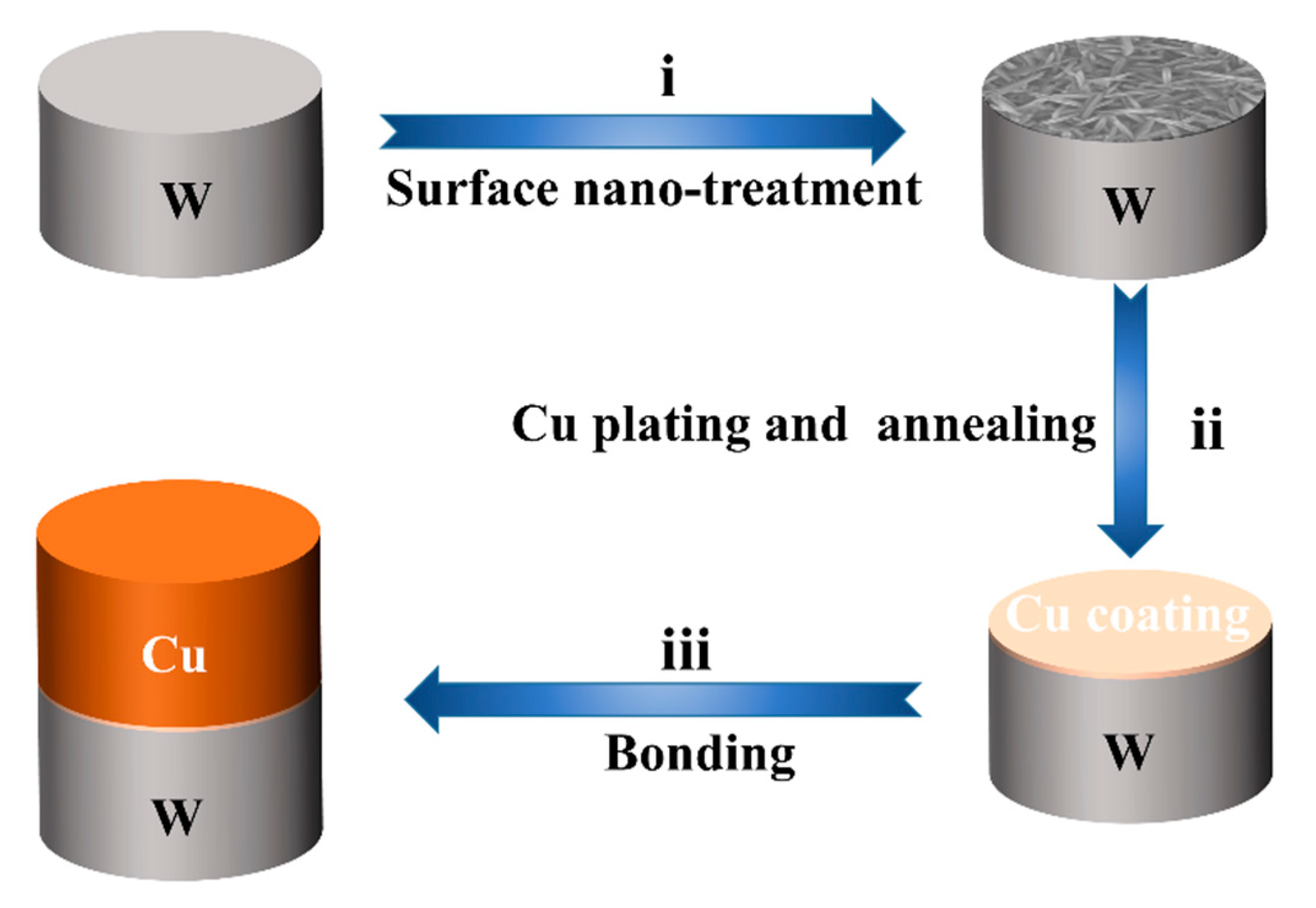
Figure 1 shows the schematic diagrams of the preparation process of W/Cu joints based on surface nano-treatment. The process includes three steps:
- surface nano-treatment of W through hydrothermal treatment and reduction annealing in an H2 atmosphere;
- Cu plating on the surface of nano-treated W, followed by annealing at 980 °C for 3 h to realize Cu penetrating;
- W/Cu bonding under a pure hydrogen atmosphere. The detailed parameters are introduced as follows.
2.1. Base Materials
In this research, commercial pure W (99.99 wt.%) rods and pure Cu (99.95 wt.%) rods with the size of Φ10 mm × 25 mm were used as original materials. The W rods and Cu rods were sanded in the proper order with waterproof abrasive papers and polished with a diamond spray polishing compound (0.25 μm) to achieve a mirror finish. The polished specimens were successively ultrasonically cleaned in acetone, ethanol, and deionized water for 15 min, and finally dried in air.
2.2. Surface Nano-Treatment
Hydrothermal treatment is one of the common methods for preparing nanostructures. Ma et al. [21] reported a method to fabricate nanostructures through a facile one-step hydrothermal treatment. Herein, the surface nano-treatment of W was achieved by hydrothermal treatment and subsequent reduction annealing. Firstly, the pretreated W rods were placed in a Teflon-lined stainless-steel autoclave, with 100 mL solution containing 15 mL 98.3% sulfuric acid, 15 mL 37% hydrochloric acid, 70 mL deionized water and 8 g chromium trioxide. The sealed autoclave was then placed into a program-controlled air oven at a set temperature of 100 °C for a predetermined time of 3 h. After autoclave cooling to temperature, the specimens were collected and rinsed with deionized water, followed by the drying process in cool air. Finally, the treated W rods were subjected to one-step reduction annealing (i.e., 700 °C for 3 h) in the pure hydrogen atmosphere.
2.3. Cu Plating and Annealing
Cu was deposited on the surface of nano-treated W specimens through the plating process. The chemical composition of the solution used for Cu plating was as follows: 25 g/L CuSO4, 170 g/L C10H14N2O8Na2·2H2O, 40 g/L NaOH, 20 g/L C2H4O6KNa·4H2O, and 4 g/L KNO3. During the deposition process, the corresponding current density was 1 A/dm2, the temperature was 40 °C, the distance between cathode and anode was 10 cm and the deposition time was 1 min and 30 min. The as-obtained W/Cu electroplating specimen was annealed at 980 °C for 3 h in the pure hydrogen atmosphere.
2.4. Bonding
Before the bonding process, the Cu rod surface was ground and polished to achieve a mirror finish. The W rods and Cu rods were assembled coaxially in a fixture made of high temperature resistant materials, as shown in Reference [22], where the copper coating side of W rods was contacted with the polished side of Cu rods. Subsequently, a pressure of 106 MPa was applied to the W-Cu assembly. Lastly, the W-Cu assemblies were placed in a tube-type furnace for annealing (i.e., 980 °C for 3 h) under a pure hydrogen atmosphere. The samples were heated to the bonding temperature at a heating rate of 10 °C/min and remained for 3 h, and then cooled naturally. When the annealing process was finished, the W/Cu joints were obtained. In addition, the W/Cu joined specimens without nano-treatment were obtained for comparison.
2.5. Characterization Methods
The bonding strength of the W/Cu joint (Φ10 mm × 50 mm) was measured via a universal testing machine at a loading rate of 1 mm/min. The tensile strength of W/Cu joining was calculated according to σ = F/S0, where F is the force loaded during the tensile test and S0 is the cross-sectional area of the tensile test sample (78.5 mm2). The strain (ε) is calculated according to ε = Δl/l0, where Δl is the displacement in the tensile process of sample, and l0 is the original length of joined W/Cu sample (50 mm).
The joined W/Cu sample was cross-sectioned using electrical discharge machining and then ground. The Vickers hardness of the W/Cu joint along the cross-section was measured via an MH-6L hardness tester under a 200 gf load for 5 s.
The phase composition of the nano-treated W specimens was analyzed using X-ray diffraction (XRD, D8Advancer, Bruker, Karlsruhe, German) with Cu Kα radiation (λ = 1.5406 Å) in the 2θ range of 20–90° at room temperature. The morphology, microstructure, and chemical composition of nano-treated W, Cu coating, and W/Cu interface were investigated by field emission scanning electron microscopy (SEM, S4800, Hitachi, Shishima, Tokyo, Japan) equipped with an energy dispersive spectrometer (EDS, X-Max 20, Oxford Instruments, Oxford, UK) detector. Lastly, the thin section of the W/Cu interface for transmission electron microscope (TEM) analysis was prepared using focused ion beam (FIB, Helios NanoLab 460HP, FEI, Hillsboro, OR, USA). The achieved samples were observed by TEM (Tecnai G2 F20 S-TWIN, FEI, Hillsboro, OR, USA) equipped with an energy-dispersive X-ray (EDX, PV97-61700, Ametek, Philadelphia, PA, USA) detector.
3. Results and Discussion
3.1. Characterization of After Surface Nano-Treatment
The morphology of W samples was investigated by SEM. As shown in Figure 2a,b, the surface of the original W before hydrothermal treatment is very flat. Figure 2c is the EDS spectrum of original W, and only the W peak exists. Figure 2d is the typical SEM image of W after hydrothermal treatment. As seen from the image, compact and uniform nanosheets formed on the entire surface region. Figure 2e shows the magnified image of the nanosheets structure in Figure 2d, indicating that the length of the formed nanosheets was about 200 nm. The EDS spectrum of the red frame region in Figure 2d is displayed in Figure 2f, where the main elements of W and O were detected. Results show that the nanosheets could be WO3, which is consistent with that reported in the literature [21]. The typical morphology of a sample after reduction annealing is shown in Figure 2g,h, which also display the nanosheets structure. Figure 2i represents the EDS spectrum of a yellow frame region in Figure 2g. Compared with the sample after hydrothermal treatment (Figure 2f), there was only one main phase of W in the sample after reduction annealing, indicating that the reduction process was sufficient. The WO3 nanosheets were completely reduced to pure W nanosheets after reduction annealing. After the nano-treatment process, nanostructures can be formed on the W surface. The existence of nanostructures can improve the surface activity of the substrate [23], which is beneficial to W/Cu bonding.
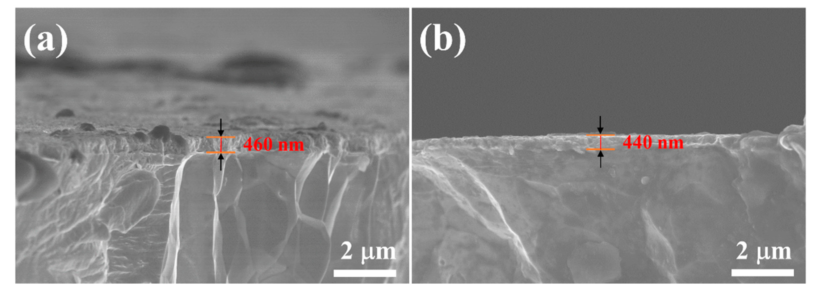
Figure 3 shows the cross-sectional SEM of a nanostructure before and after the reduction annealing process. As shown in Figure 3a, the thickness of tungsten oxide formed before the reduction annealing process was about 460 nm. Figure 3b shows the cross-sectional morphology of the nano-treated W structure after reduction annealing. The depth of nano-treated W structure after reduction annealing was approximately 440 nm.
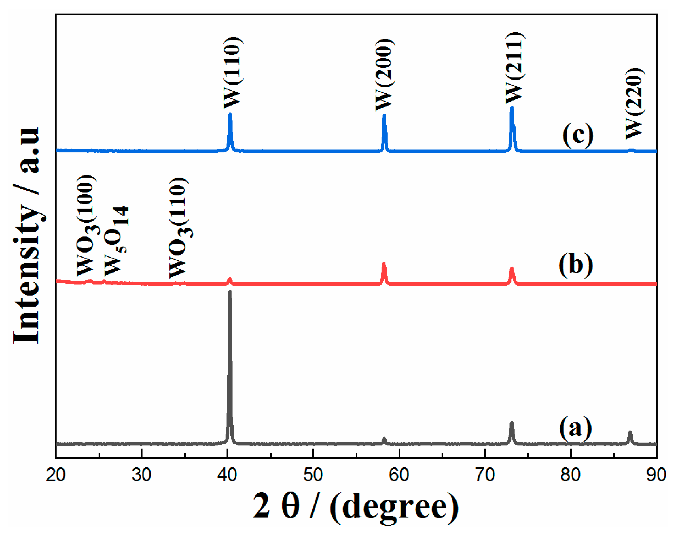
Figure 4 shows the XRD patterns of W base material after hydrothermal treatment, and after hydrothermal treatment and reduction annealing. It can be seen from Figure 4a that the W base materials showed diffraction peaks corresponding to W(110), W(200), W(211), and W(220). After hydrothermal treatment, the diffraction peaks of WO3(100), WO3(110), and W5O14 were observed, implying that W was partially oxidized to WO3 and W5O14 during hydrothermal treatment. After hydrothermal treatment and reduction annealing, there was only the W phase, and no tungsten oxide phase appeared, indicating that the oxygen impurity was removed completely [24]. The XRD analysis results agree with the EDS results in Figure 2i. The peak intensities have changed significantly, indicating the crystalline orientation of nano-treated W has changed. This is caused by the growth of the nanosheets structure along different crystal planes during hydrothermal treatment.
3.2. Morphology and EDS Analysis of Cu Plating
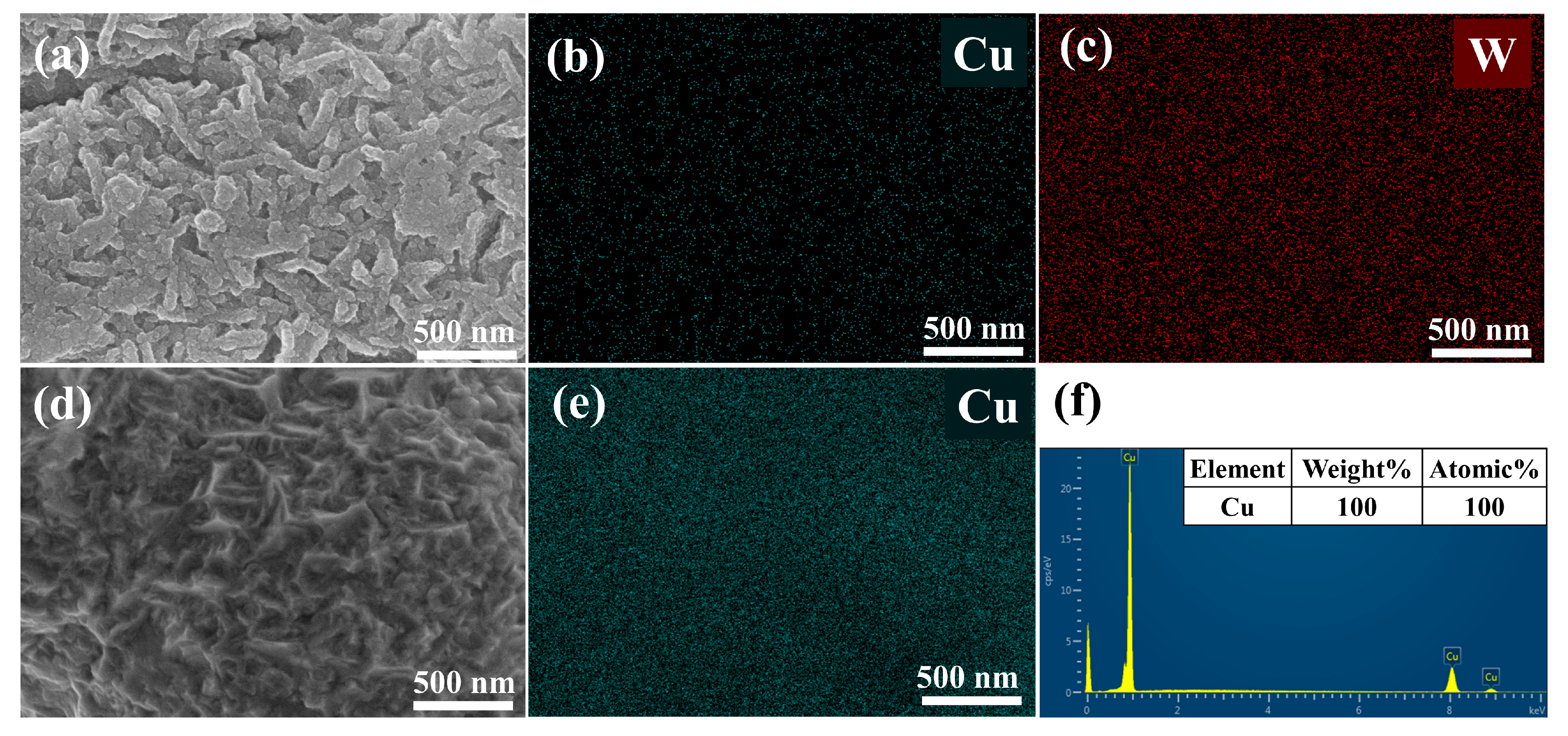
Figure 5 shows the surface morphology and the EDS results of Cu plating for 1 min and 30 min. As shown in Figure 5a, after Cu plating for 1 min, the electroplating Cu particles partially covered the surface of the nanosheets W substrate, and the gaps between nanosheets were filled by the electroplated Cu particles. Nanostructures formed on the surface of W increase the specific surface of W [24]. After Cu plating, the electrodeposited Cu particles embedded in the nano-treated W structure, which increases the contact area of W and Cu. At this time, a mechanical inlay effect formed between electroplating Cu particles and the nano-treated W structure. According to the corresponding mapping results (see Figure 5b,c), the electroplating Cu particles were uniformly distributed. In addition, there was a large amount of W, implying that the plating time was insufficient and the formed copper plating layer did not completely cover the base material. After Cu plating for 30 min, the surfaces were completely covered by a Cu layer (see Figure 5d). As shown in Figure 5e, the elemental mapping in Figure 5d only contained Cu, which is due to the surface being covered completely by a Cu layer. Finally, after Cu plating for 30 min, a dense Cu layer deposited on the surface of nano-treated W.
Figure 6a shows the surface morphology of nano-treated W after Cu plating for 30 min and then annealing at 980 °C for 3 h. It can be seen from Figure 6a that the obtained W/Cu electroplating sample exhibited a dense and smooth surface layer with the average size of about 8 μm after annealing. As shown in Figure 6b, the obtained Cu coating was about 5 μm thick after annealing. Moreover, based on the EDS line scan result, the Cu coating tightly combined with W substrate. The electrodeposited Cu on the nano-treated W surface wetted the surface structures uniformly and formed a compact W/Cu interface after the annealing process, thus establishing a good foundation for W/Cu bonding. During the W/Cu bonding process, the electrodeposited Cu coating plays the role of the interlayer metal.
3.3. Tensile Strength and Microstructure Characterization of W/Cu Joints
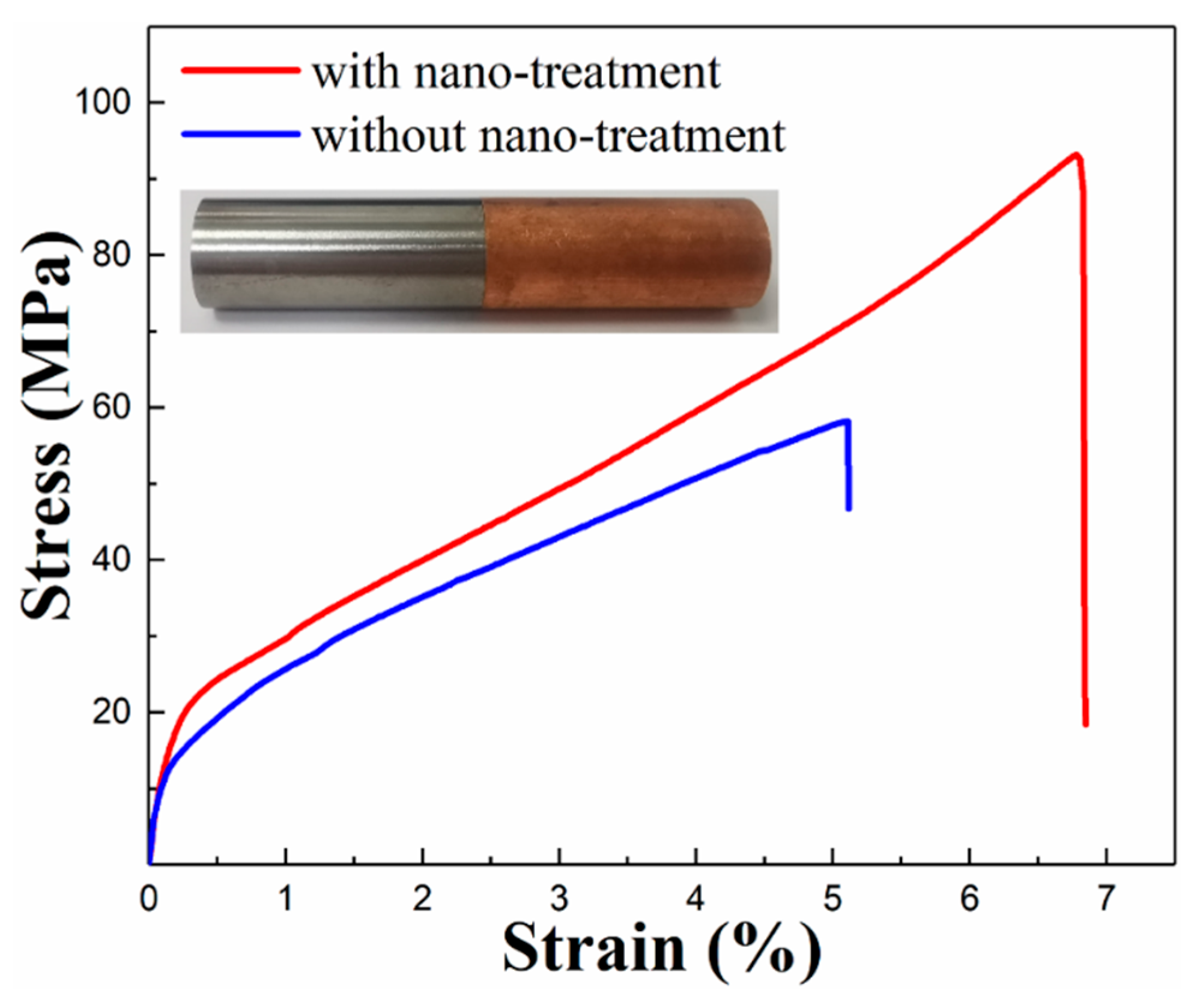
Figure 7 shows the as-obtained W/Cu joint and tensile strength test results. It can be seen from Figure 7 that, when the W substrates were not nano-treated, the tensile strength of W/Cu joints only reached about 58 MPa. However, for the W/Cu joint prepared with nano-treatment, the tensile strength reached as high as about 93 MPa, which increased by approximately 60% compared with the one without nano-treatment. Evidently, the W/Cu bonding strength was enhanced significantly by nano-treatment and Cu embedding. For W/Cu bonding with a nanostructure and Cu plating, the Cu particles embedded in the nano-treated W structures formed micro-protrusions after annealing. In the process of W/Cu interface separation, more energy was needed to pull the micro-protrusion compared with the W/Cu joints with flat interface, which contributes to the improvement of the W/Cu bonding strength. Additionally, the W/Cu joints (the inset) obtained at 980 °C had good concentricity and a smooth appearance, and there were no obvious shape changes in the specimen.
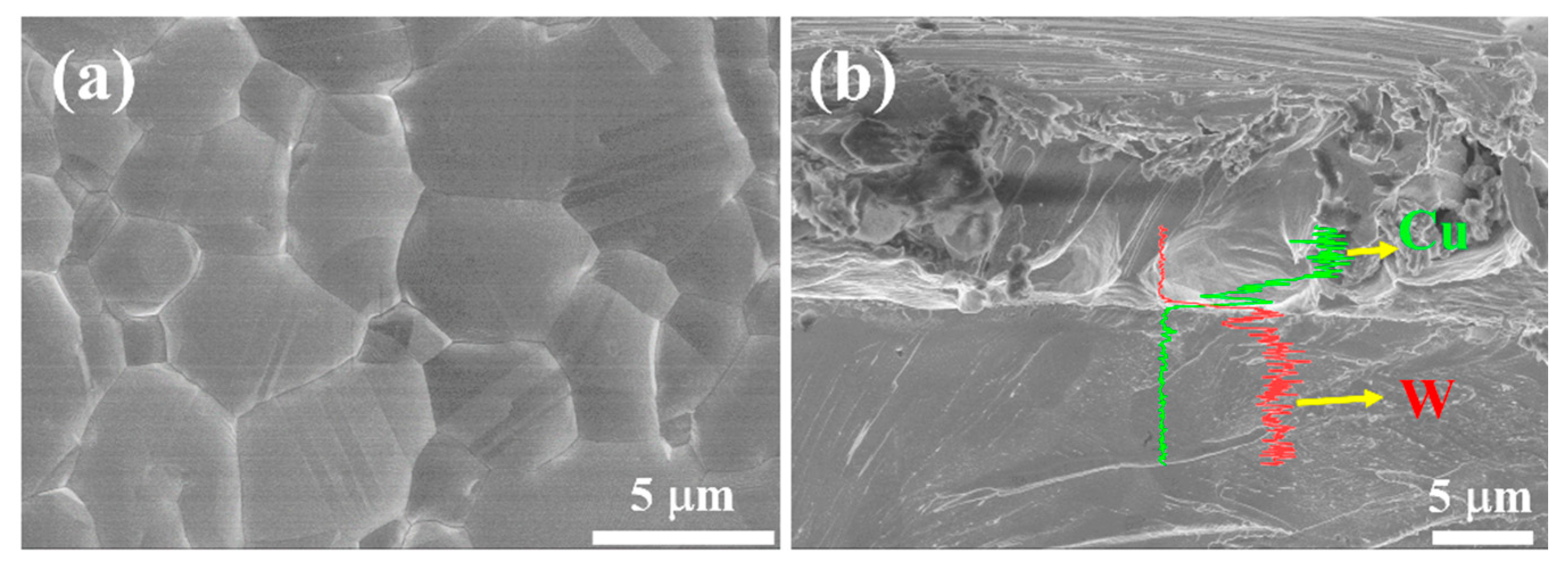
The microstructure of the W/Cu joints achieved at 980 °C for 3 h is displayed in Figure 8a. Figure 8a highlights a tight bond between W and Cu, and no gap was found in the W/Cu joint, indicating the joining was successfully realized. The distribution of microhardness values along the cross-section of the W/Cu joint is shown as a graphical plot in Figure 8b. The minimum hardness value (~56 HV) was obtained at the Cu side, and the maximum hardness value (~ 470 HV) was obtained at the W side. The microhardness curves exhibited continuous changes along the W/Cu interface, which would be in favor of relaxing residual stress of bonded W/Cu joints [15,25].
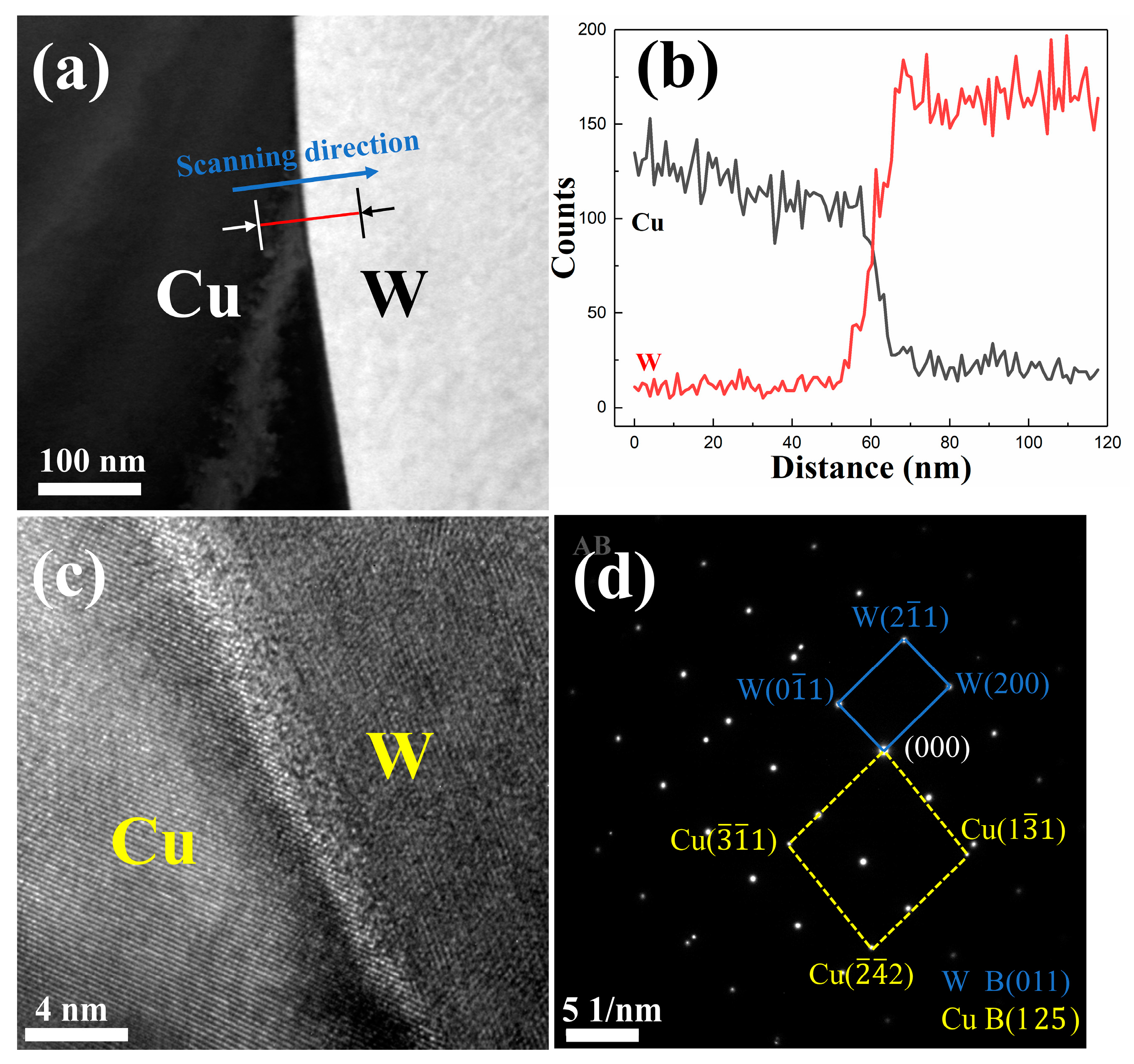
Due to W and Cu immiscibility, it is important to investigate the interface structure between W and Cu. The microstructure characterization results of the W/Cu interface are presented in Figure 9. As shown in Figure 9a, the W/Cu interface was compact without any cracks or voids. Figure 9b shows the EDX line scanning compositional profile of the W/Cu interface along the red line marked in Figure 9a. It can be seen from Figure 9b that a concentration gradient distribution formed at the W/Cu interface. This result may be attributed to Cu penetrating the nano-treated W surface, forming an area where W and Cu coexist. Additionally, the HRTEM image of the W/Cu interface shown in Figure 9b implies that the W atoms and Cu atoms had good bonding at W/Cu interface. The SAED pattern presented in Figure 9d shows that the W/Cu interface was composed of W and Cu crystalline structures. These results suggest that a well-cohesive W/Cu interface was formed using the three-step bonding process in this work.
In summary, nano-treatment and Cu penetrating before the bonding process effectively enhanced the bonding strength. The method proposed in this paper can be applied for enhancing the bonding strength of immiscible materials, including, but not limited to, W and Cu.
4. Conclusions
In this study, high-strength bonding of immiscible W and Cu is achieved through a three-step bonding process:
- surface nano-treatment;
- Cu plating followed by annealing at high temperature;
- bonding process. The nano-treatment of W was achieved through hydrothermal treatment and subsequent reduction annealing at 700 °C for 3 h.
Nanosheets structure can be found on W substrate surface. The nano-treatment and Cu penetrating lay a good foundation for the subsequent bonding process. After bonding at 980 °C for 3 h, the tensile strength of the W/Cu joint fabricated with nano-treatment reached as high as about 93 MPa, which increased by about 60% compared with the W/Cu joint prepared without nano-treatment. The microhardness curves exhibited continuous changes along the W/Cu interface. The TEM images show that W/Cu interface was compact without any cracks or voids. The bonding technology proposed in this paper can be applied for enhancing the bonding strength of immiscible materials, including, but not limited to, W and Cu.
Author Contributions
Conceptualization, F.L. and Y.H.; methodology, F.L. and Y.H.; software, F.L. and X.C.; validation, F.L., X.C. and C.L.; formal analysis, F.L., X.C. and Y.C.; investigation, F.L.; resources, Y.H.; data curation, Y.H.; writing—original draft preparation, F.L.; writing—review and editing, Y.C., X.C., C.L. and Y.H.; visualization, F.L.; supervision, Y.H.; project administration, Y.H.; funding acquisition, Y.H. All authors have read and agreed to the published version of the manuscript.
Funding
This research was funded by the National Key Research and Development Program of China (Grant Nos. 2018YFB0703904 and 2017YFE0302600) and the National Natural Science Foundation of China (Grant No. 51471114).
Data Availability Statement
The raw/processed data required to reproduce these findings can be found in this paper.
Acknowledgments
The authors are grateful to Li You for help in TEM sample preparation.
Conflicts of Interest
The authors declare no conflict of interest.
References
- Philipps, V. Tungsten as Material for Plasma-Facing Components in Fusion Devices. J. Nucl. Mater. 2011, 415, S2–S9. [Google Scholar] [CrossRef]
- Ueda, Y.; Coenen, J.W.; De Temmerman, G.; Doerner, R.P.; Linke, J.; Philipps, V.; Tsitrone, E. Research Status and Issues of Tungsten Plasma Facing Materials for ITER and Beyond. Fusion Eng. Des. 2014, 89, 901–906. [Google Scholar] [CrossRef]
- Huang, P.; Wang, Y.; Peng, H.; Chen, J.; Wang, P. Diffusion Bonding W and RAFM-Steel with an Fe Interlayer by Hot Isostatic Pressing. Fusion Eng. Des. 2020, 158, 111796. [Google Scholar] [CrossRef]
- Hu, W.; Dong, Z.; Wang, H.; Ahamad, T.; Ma, Z. Microstructure Refinement and Mechanical Properties Improvement in the W-Y2O3 Alloys via Optimized Freeze-Drying. Int. J. Refract. Met. Hard Mater. 2021, 95, 105453. [Google Scholar] [CrossRef]
- Hu, W.; Kong, X.; Du, Z.; Khan, A.; Ma, Z. Synthesis and Characterization of Nano TiC Dispersed Strengthening W Alloys via Freeze-Drying. J. Alloys Compd. 2021, 859, 157774. [Google Scholar] [CrossRef]
- Saito, S.; Fukaya, K.; Ishiyama, S.; Sato, K. Mechanical Properties of HIP Bonded W and Cu-Alloys Joint for Plasma Facing Components. J. Nucl. Mater. 2002, 307, 1542–1546. [Google Scholar] [CrossRef]
- Bolt, H.; Barabash, V.; Krauss, W.; Linke, J.; Neu, R.; Suzuki, S.; Yoshida, N.; Team, A.U. Materials for the Plasma-Facing Components of Fusion Reactors. J. Nucl. Mater. 2004, 329, 66–73. [Google Scholar] [CrossRef] [Green Version]
- Mitteau, R.; Missiaen, J.M.; Brustolin, P.; Ozer, O.; Durocher, A.; Ruset, C.; Lungu, C.P.; Courtois, X.; Dominicy, C.; Maier, H.; et al. Recent Developments Toward the Use of Tungsten as Armour Material in Plasma Facing Components. Fusion Eng. Des. 2007, 82, 1700–1705. [Google Scholar] [CrossRef] [Green Version]
- Xi, S.; Zuo, K.; Li, X.; Ran, G.; Zhou, J. Study on the Solid Solubility Extension of Mo in Cu by Mechanical Alloying Cu With Amorphous Cr(Mo). Acta Mater. 2008, 56, 6050–6060. [Google Scholar] [CrossRef]
- Chapa, J.; Reimanis, I. Modeling of Thermal Stresses in a Graded Cu/W Joint. J. Nucl. Mater. 2002, 303, 131–136. [Google Scholar] [CrossRef]
- Zhao, P.; Guo, S.; Liu, G.; Chen, Y.; Li, J. Fabrication of W-Cu Functionally Graded Material with Improved Mechanical strength. J. Alloys Compd. 2014, 601, 289–292. [Google Scholar] [CrossRef]
- Chen, W.; Dong, L.; Zhang, H.; Song, J.; Deng, N.; Wang, J. Microstructure Characterization of W-Cu Alloy Sheets Produced by High Temperature and High Pressure Deformation Technique. Mater. Lett. 2017, 205, 198–201. [Google Scholar] [CrossRef]
- Batra, I.S.; Kale, G.B.; Saha, T.K.; Ray, A.K.; Derose, J.; Krishnan, J. Diffusion Bonding of a Cu–Cr–Zr Alloy to Stainless Steel and Tungsten Using Nickel as an Interlayer. Mater. Sci. Eng. A 2004, 369, 119–123. [Google Scholar] [CrossRef]
- Chong, F.L.; Chen, J.L.; Li, J.G. Thermal Analysis of Tungsten Coating on CuCrZr with Different Interlayers Used as EAST Divertor Target Materials. Mater. Des. 2008, 29, 1675–1678. [Google Scholar] [CrossRef]
- Yan, H.; Fan, J.; Han, Y.; Yao, Q.; Liu, T.; Lv, Y.; Zhang, C. Vacuum Diffusion Bonding W to W-Cu Composite: Interfacial Microstructure and Mechanical Properties. Vacuum 2019, 165, 19–25. [Google Scholar] [CrossRef]
- Wang, S.; Ling, Y.; Wang, J.; Xu, G. Microstructure and Mechanical Properties of W/Cu Vacuum Diffusion Bonding Joints Using Amorphous Fe–W Alloy as Interlayer. Vacuum 2015, 114, 58–65. [Google Scholar] [CrossRef]
- Du, J.; Huang, Y.; Liu, J.; Liu, Y.; Wang, Z. Irradiation Damage Alloying for Immiscible Alloy Systems and its Thermodynamic Origin. Mater. Des. 2019, 170, 107699. [Google Scholar] [CrossRef]
- Ermolenko, A.S.; Korolev, A.V.; Gerasimov, E.G.; Gaviko, V.S. Magnetic Field Induced Ferromagnetism in Pseudobinary PrAl2−xNix Alloys. J. Magn. Magn. Mater. 2016, 404, 133–142. [Google Scholar] [CrossRef]
- Zhang, J.; Huang, Y.; Liu, Y.; Wang, Z. Direct Diffusion Bonding of Immiscible Tungsten and Copper at Temperature Close to Copper’s Melting Point. Mater. Des. 2018, 137, 473–480. [Google Scholar] [CrossRef]
- Jiang, D.; Long, J.; Cai, M.; Lin, Y.; Fan, P.; Zhang, H.; Zhong, M. Femtosecond Laser Fabricated Micro/Nano Interface Structures Toward Enhanced Bonding Strength and Heat Transfer Capability of W/Cu joining. Mater. Des. 2017, 114, 185–193. [Google Scholar] [CrossRef]
- Ma, Z.; Hou, H.; Song, K.; Fang, Z.; Wang, L.; Gao, F.; Yang, W.; Tang, B.; Kuang, Y. Engineering Oxygen Vacancies by One-Step Growth of Distributed Homojunctions to Enhance Charge Separation for Efficient Photoelectrochemical Water Splitting. Chem. Eng. J. 2020, 379, 122266. [Google Scholar] [CrossRef]
- Du, J.; Huang, Y.; Xiao, C.; Liu, Y. Building Metallurgical Bonding Interfaces in an Immiscible Mo/Cu System by Irradiation Damage Alloying (IDA). J. Mater. Sci. Technol. 2018, 34, 689–694. [Google Scholar] [CrossRef]
- Chen, X.; Zhang, P.; Liu, Y.; Wang, Z.; Huang, Y. Nanoconical Active Structures Prepared by Anodization and Deoxidation of Molybdenum Foil and Their Activity Origin. J. Alloys Compd. 2021, 851, 156896. [Google Scholar] [CrossRef]
- Zhang, J.; Huang, Y.; Wang, Z.; Liu, Y. Preparation of a Nanoporous Active Tungsten Foil By Two-Step Anodizing and Deoxidized Annealing for Hydrogen Evolution Reaction. Nanotechnology 2019, 30, 015603. [Google Scholar] [CrossRef]
- Zhao, P.; Wang, S.; Guo, S.; Chen, Y.; Ling, Y.; Li, J. Bonding W and W–Cu Composite With an Amorphous W–Fe Coated Copper Foil Through Hot Pressing Method. Mater. Des. 2012, 42, 21–24. [Google Scholar] [CrossRef]
Figure 1.
Schematic diagrams of the preparation process of W/Cu joints based on surface nano-treatment.
Figure 1.
Schematic diagrams of the preparation process of W/Cu joints based on surface nano-treatment.

Figure 2.
SEM images of the surface morphology and the corresponding EDS results of W surface: (a–c) before hydrothermal treatment, (d–f) after hydrothermal treatment, and (g–i) after hydrothermal treatment and reduction annealing process.
Figure 2.
SEM images of the surface morphology and the corresponding EDS results of W surface: (a–c) before hydrothermal treatment, (d–f) after hydrothermal treatment, and (g–i) after hydrothermal treatment and reduction annealing process.

Figure 3.
Cross-sectional SEM of (a) tungsten oxide formed before the reduction annealing process, and (b) nano-treated W structure after reduction annealing.
Figure 3.
Cross-sectional SEM of (a) tungsten oxide formed before the reduction annealing process, and (b) nano-treated W structure after reduction annealing.

Figure 4.
XRD patterns of W: (a) base materials, (b) after hydrothermal treatment, and (c) after hydrothermal treatment and reduction annealing.
Figure 4.
XRD patterns of W: (a) base materials, (b) after hydrothermal treatment, and (c) after hydrothermal treatment and reduction annealing.

Figure 5.
SEM images of the surface morphology and the corresponding EDS results of Cu plating for (a) 1 min; (b) and (c) elemental mapping in (a); (d) 30 min; (e) element mapping and (f) EDS results in (d).
Figure 5.
SEM images of the surface morphology and the corresponding EDS results of Cu plating for (a) 1 min; (b) and (c) elemental mapping in (a); (d) 30 min; (e) element mapping and (f) EDS results in (d).

Figure 6.
SEM image of nano-treated W after Cu plating for 30 min and then annealing at 980 °C for 3 h: (a) surface morphology, (b) cross-section morphology and EDS line scan image.
Figure 6.
SEM image of nano-treated W after Cu plating for 30 min and then annealing at 980 °C for 3 h: (a) surface morphology, (b) cross-section morphology and EDS line scan image.

Figure 7.
The stress-strain curves of W/Cu joints prepared with nano-treatment and without nano-treatment. The inset demonstrates typical tensile test sample.
Figure 7.
The stress-strain curves of W/Cu joints prepared with nano-treatment and without nano-treatment. The inset demonstrates typical tensile test sample.

Figure 8.
(a) The microstructure of the W/Cu joint achieved at 980 °C for 3 h with nano-treatment, (b) Vickers microhardness distribution along the cross-section of the W/Cu joint.
Figure 8.
(a) The microstructure of the W/Cu joint achieved at 980 °C for 3 h with nano-treatment, (b) Vickers microhardness distribution along the cross-section of the W/Cu joint.

Figure 9.
Microscopic characterization for the cross-section of the W/Cu joints: (a) drift corrected spectrum profile, (b) EDX line-scanning profile along the red-line in (a), (c) HRTEM image at the interface, and (d) selected area diffraction pattern.
Figure 9.
Microscopic characterization for the cross-section of the W/Cu joints: (a) drift corrected spectrum profile, (b) EDX line-scanning profile along the red-line in (a), (c) HRTEM image at the interface, and (d) selected area diffraction pattern.

Publisher’s Note: MDPI stays neutral with regard to jurisdictional claims in published maps and institutional affiliations. |
© 2021 by the authors. Licensee MDPI, Basel, Switzerland. This article is an open access article distributed under the terms and conditions of the Creative Commons Attribution (CC BY) license (https://creativecommons.org/licenses/by/4.0/).
Share and Cite
MDPI and ACS Style
Li, F.; Chen, Y.; Chen, X.; Li, C.; Huang, Y. The Improvement of Bonding Strength of W/Cu Joints via Nano-Treatment of the W Surface. Metals 2021, 11, 844. https://0-doi-org.brum.beds.ac.uk/10.3390/met11050844
AMA Style
Li F, Chen Y, Chen X, Li C, Huang Y. The Improvement of Bonding Strength of W/Cu Joints via Nano-Treatment of the W Surface. Metals. 2021; 11(5):844. https://0-doi-org.brum.beds.ac.uk/10.3390/met11050844
Chicago/Turabian StyleLi, Fei, Yuanyuan Chen, Xin Chen, Cai Li, and Yuan Huang. 2021. "The Improvement of Bonding Strength of W/Cu Joints via Nano-Treatment of the W Surface" Metals 11, no. 5: 844. https://0-doi-org.brum.beds.ac.uk/10.3390/met11050844
Note that from the first issue of 2016, this journal uses article numbers instead of page numbers. See further details here.