Dielectric Elastomer Actuator-Based Multifunctional Smart Window for Transparency Tuning and Noise Absorption


1
Temasek Laboratories, National University of Singapore, Singapore 117411, Singapore
2
Department of Mechanical Engineering, National Chiao Tung University, Hsinchu 30010, Taiwan
3
d’Optron Pte Ltd., 71 Nanyang Avenue, Singapore 638075, Singapore
4
School of Aeronautics and Astronautics, Sun Yat-Sen University, Shenzhen 518107, China
*
Author to whom correspondence should be addressed.
Actuators 2021, 10(1), 16; https://0-doi-org.brum.beds.ac.uk/10.3390/act10010016
Submission received: 21 December 2020
/
Revised: 12 January 2021
/
Accepted: 12 January 2021
/
Published: 15 January 2021
(This article belongs to the Special Issue Selected Papers from the 1st International Electronic Conference on Actuator Technology: Materials, Devices and Applications (IeCAT))
Abstract
:Soft actuators are compliant material-based devices capable of producing large deformation upon external stimuli. Dielectric elastomer actuators (DEA) are a type of soft actuator that operates on voltage stimuli. Apart from soft robotics, these actuators can serve many novel applications, for example, tunable optical gratings, lenses, diffusers, smart windows and so on. This article presents our current work on tunable smart windows which can regulate the light transmittance and the sound absorption. This smart window can promote daylighting while maintaining privacy by electrically switching between transparent and opaque. As a tunable optical surface scatters, it turns transparent with smooth surfaces like a flat glass; but it turns ‘opaque’ (translucent) with the micro-rough surface. The surface roughness is varied employing surface micro-wrinkling or unfolding using dielectric elastomer actuation. Moreover, this smart window is equipped with another layer of transparent micro-perforated dielectric elastomer actuator (DEA), which acts like Helmholtz resonators serving as a tunable and broader sound absorber. It can electrically tune its absorption spectrum to match the noise frequency for maximum acoustic absorption. The membrane tension and perforation size are tuned using DEA activation to tune its acoustic resonant frequency. Such a novel smart window can be made as cheap as glass due to its simple all-solid-state construction. In future, they might be used in smart green buildings and could potentially enhance urban livability.
1. Introduction
Glass panels are widely used as transparent facades to buildings. They are optically transparent to allow daylighting while being acoustic barriers, they isolate the outdoor noise. However, these transparent glasses make the privacy of the buildings vulnerable. Besides, the glass panels are not effective at damping out indoor noise or echoes that reverberate in the event of indoor musical performance or public announcements. Therefore, there is a need for window solutions that can regulate visibility and sufficiently absorb sound as well. Curtains are the simplest solution to achieve both functionalities. Thick textile curtains are often used to block visibility for privacy purpose. They can also act like porous acoustic absorbers to attenuate indoor noise [1]. Yet, they are unable to provide both functionalities sufficiently and simultaneously. For example, they cannot absorb sound when they are open to allow daylight in. There are few translucent sound-absorbing curtains, [2] but they are relatively poor at sound absorption and they still block visibility.
There are different types of glass which provide either one of these functionalities. For example, there are smart window solutions that can switch between transparent and opaque or translucent as desired. These commercial smart windows are based on electrochromic [3,4], polymer-dispersed liquid crystal (PDLC) devices [5,6] and suspended particle devices (SPD) [7]. Electrochromic devices in a battery construction change colour and thus light absorption coefficient upon electrical stimuli. PDLC devices consist of the liquid crystals immersed in the polymer matrix. The random orientations of these liquid crystals are electrically controlled to switch between milky and clear states. SPD has light-absorbing particles whose distribution is also electrically controlled to adjust the transmission of light. However, these devices are costly to adopt for large-area windows [3]. Their manufacturing cost is high ($200 per square foot) due to complex construction. Moreover, their adoption is hindered by other issues. For example, electrochromic windows are subject to a slow response (taking 5 min for switching a 0.01 square meter panel) and fast ageing; whereas, PLDC and SPD only show a moderate transparency tuning range (50–80%) and are not so transparent at their clear state [7]. Moreover, they continuously consume high power when switched to be transparent. Low-cost transparency switching devices based on tunable optical diffusers seem promising. Some are electrically tunable using dielectric elastomer actuators [8,9]. However, reported devices are far from applicable due to large strain involvement and narrow tuning range [8,9,10,11,12].
Similarly, there are few transparent glass solutions to minimize reverberation of indoor noise [13,14,15]. For example, panel absorbers can be transparent, but they have a narrow absorption frequency bandwidth [16]. Microperforated panel (MPP) absorbers have slightly broader absorption frequency bandwidth. However, they are still fixed and are unable to absorb sound beyond their absorption bandwidth. These passive absorbers are inefficient when absorbing sound that outlies their absorption bandwidth and unable to adapt to varying noise frequency.
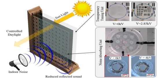
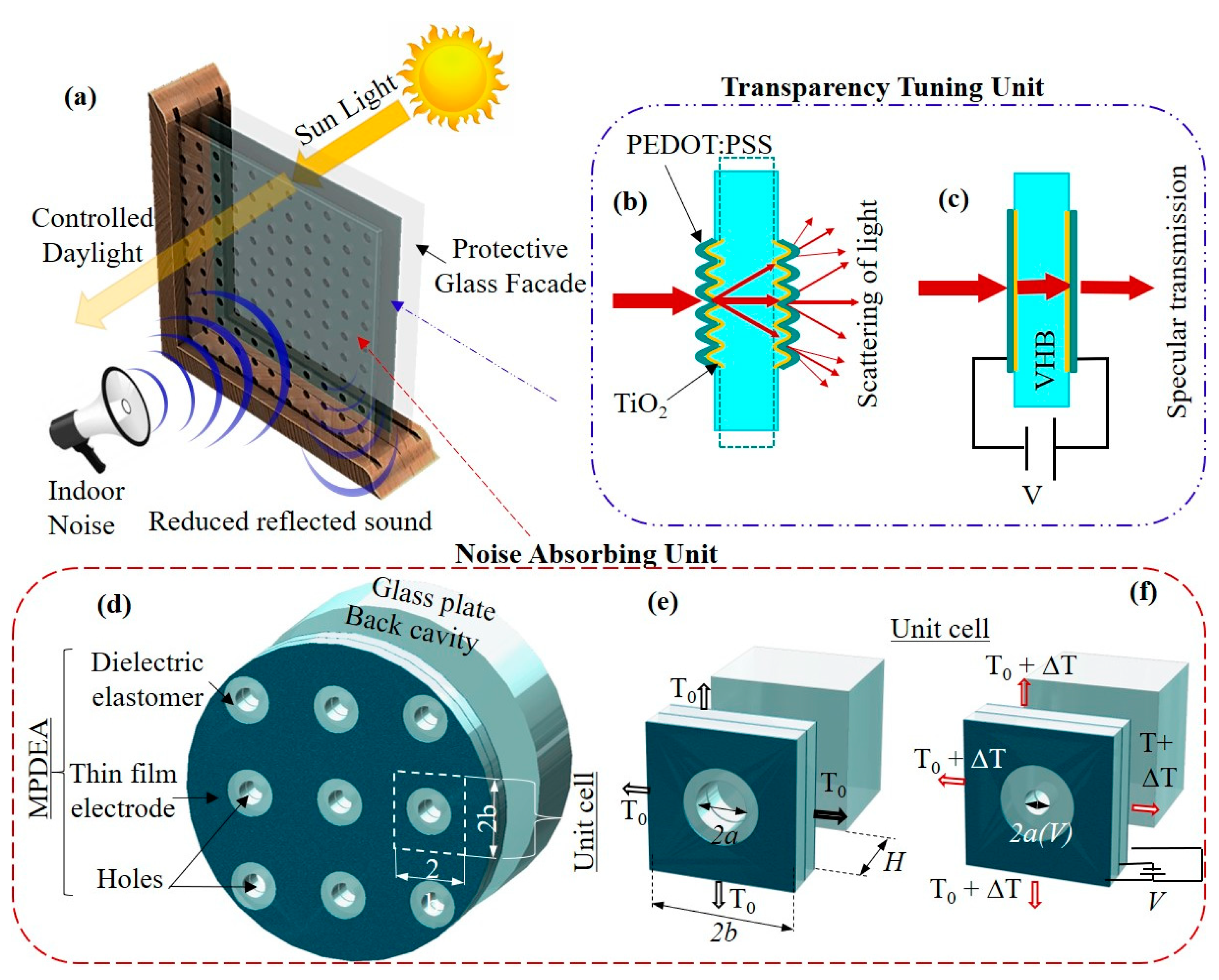
Currently, no window appliance can regulate natural daylight in a building, tune the transparency for privacy and sufficiently absorb indoor noise to reduce its reverberation simultaneously at a reasonable price. The article presents a concept of such low-cost smart window based on dielectric elastomer actuators (DEAs). This work explores micro-wrinkling of hybrid multilayer electrode made of titanium dioxide (TiO2) thin film and polymeric conductive thin films made of poly(3,4-ethylenedioxythiophene) polystyrene sulfonate (PEDOT:PSS). This is used to develop a tunable optical diffuser which requires a low activation strain for transparency switching. This elastomeric tunable optical diffuser shall meet the stringent requirements for high transmittance in the clear state, a very low transmittance at the translucent state, fast response, and long life for repeated cycles. Moreover, this work addresses the need for the transparent and tunable broadband acoustic absorber. We used transparent micro-perforated membranes to make a relatively broadband acoustic absorber. Also, the dielectric elastomer actuator is used to make this absorber tunable. Hence, they can tune their absorption spectrum and maintain optimal absorption of the noise with changing dominant frequency. Eventually, these two DEA-based components are combined for two functionalities. The first layer provides the transparency switching capability and the second layer provides the tunable broadband noise absorption (see Figure 1a).
2. Theory
This article presents DEA for two functionalities. Figure 1 shows that the sound-absorbing unit consists of the microperforated dielectric elastomer actuator (MPDEA) and a rigid backplate (such as glass), and the transparency tuning unit is a thin membrane that can be placed between the MPDEA and the backplate. The transparency tuning device is made of tunable optical diffuser consisting of two tunable optical scatterer surfaces sandwiching a dielectric elastomer membrane (see Figure 1a–c). Its surface topography changes due to microwrinkling can tune the scattering of forward visible light [17,18]. The details on the microwrinkling are given in the Supplementary text S.2.1. For a smooth surface, the total transmittance at normal incidence is: T = 1 − R = (4n1 n2)(n2 + n1)2) according to Fresnel equations. Here, R is total reflectance, n1 and n2 are the refractive indexes of the optical medium in which light is travelling. Consider a device with two identical Gaussian surfaces of voltage-tunable roughness σ(V) and finite electrical conductivity. The specular (non-diffuse) part of the total transmittance through the device is obtained as [19,20,21]:
where n1 = 1 for air and n2 being greater than 1 for elastomer substrate and λ is the wavelength of the light. The surface roughens upon formation of microwrinkle under biaxial compression of the electrodes which is achieved by releasing pre-stretch of the elastomer substrate. Dielectric elastomer actuation can unfold these initially microwrinkled surfaces of compliant electrodes. Application of high voltage V across the dielectric membrane of thickness ts induces a compressive electrostatic pressure Pe = εrεo(V/ts)2, where εr is the dielectric constant and εo is the permittivity of vacuum [22,23]. Due to Poisson’s ratio effect, electrostatically squeezed membrane expands in the area (for further information see Section S.2). Hence, this voltage-induced areal expansion can reduce the compressive strain in the thin-film electrodes. Consequently, it reduces the surface roughness turning the membrane optically clear.
Meanwhile, Figure 1d shows the smart transparent acoustic absorption unit, which consists of a MPDEA and a 40 mm deep back-cavity covered by a rigid transparent plate. The MPDEA consists of a micro-perforated membrane of dielectric elastomer sandwiched by a pair of transparent polymeric compliant electrodes. The high voltage activation of MPDEA reduces the bi-axial pre-stress T0 in the membrane by ∆T(V) such that the remaining tension becomes
where ν is the Poisson’s ratio of dielectric elastomer membrane (typically with a value of 0.5) according to reference [24] on the assumption of small elastic strain. Activation of the annular dielectric elastomer that surrounds the passive hole can reduce the hole radius by ∆a(V) following reference [25,26,27,28]:
where b is the half-pitch between holes (i.e., b = 2.5 mm) (see Figure 1d–f) (see Supplementary S2.1 for detailed formulation).
A micro-perforated membrane acoustic absorber can be roughly represented by unit cells of Helmholtz resonators [29,30,31]. A Helmholtz resonator is a container of air with a neck-like open hole. When disturbed by the sound, the air in the container or the open hole can vibrate and bounces at a fixed resonant frequency (like a spring-mass system does) to dissipate acoustic energy into heat. According to reference [31], this resonant frequency of air vibration is determined from the formula:
where c is the sound speed, A and L are the cross-sectional area and length of the neck-like open hole, and S is the volume space of the air container. Here, the hole size, i.e., A = A(V) = πa2(V) and L = L(V) is electrically tunable by a dielectric elastomer actuator [32,33]. A more detailed and precise theoretical model of such microperforated membrane absorber has been added in the Supplementary text 3.0. This model was adapted from C. Li et al. [34] and is verified in previous publications as well [25].
3. Experiments
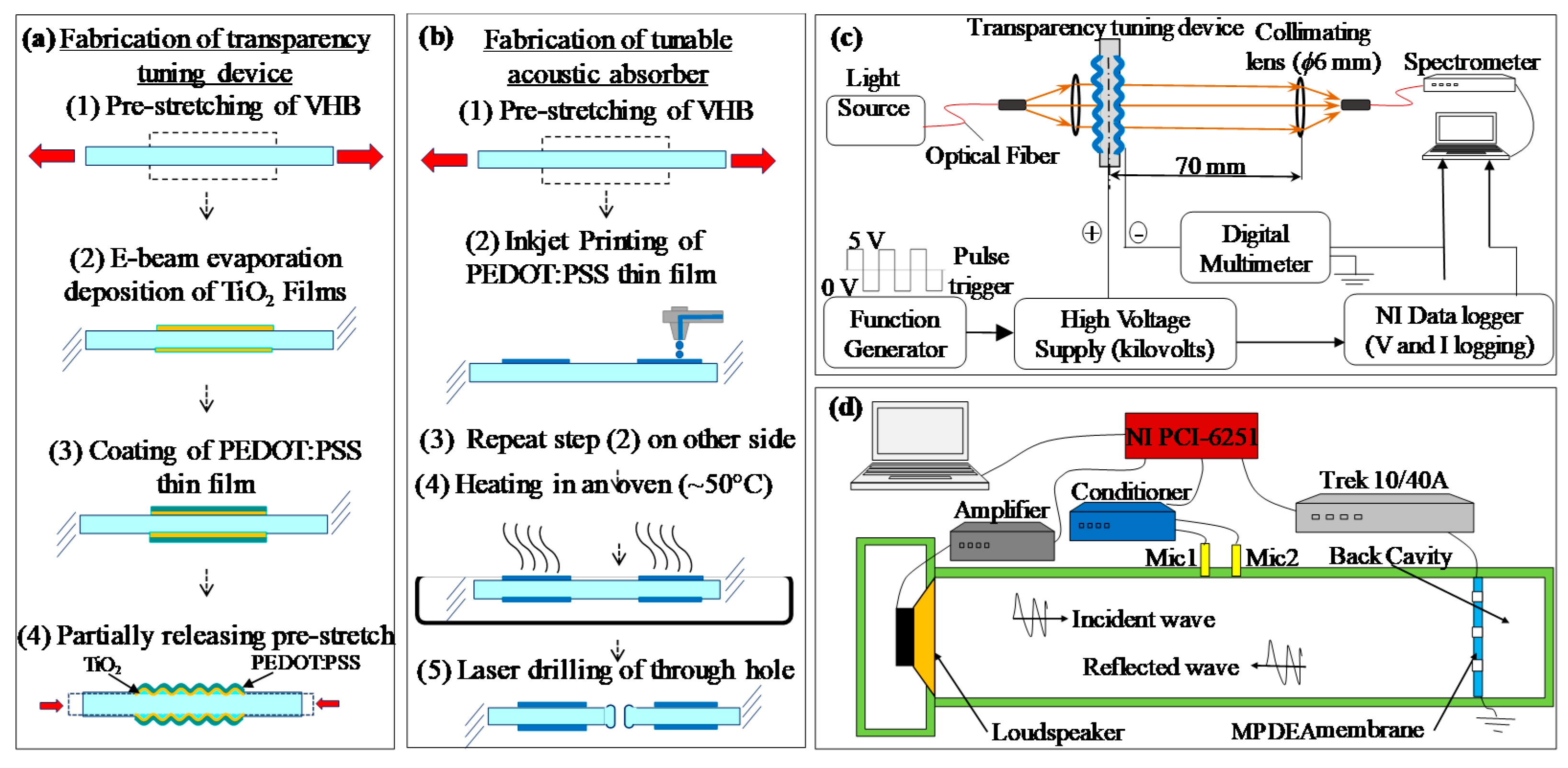
Fabrication of this multifunctional smart window follows the same procedures as making a dielectric electrode actuator. However, a transparency tunable window device uses microwrinkled electrodes, [35] which involves the special use of TiO2 and PEDOT:PSS nanometric thin films as the surface scatterer. The TiO2 layer provides the required stiffness to form large wrinkles at lower compressive strain and the PEDOT:PSS layer gives this multilayer system the electrical conductivity for electrical activation. Fabrication steps include (see Figure 2a): (1) biaxially pre-stretching tape of acrylate elastomer (3M VHB4905) elastomer membrane substrate three times; (2) e-beam evaporation of 19.8 nm thick TiO2 film; (3) spin coating of 38.79 nm thick PEDOT:PSS film at 1000 rpm for 1 min (Clevios P Jet HC V2, from Heraeus Deutschland GmbH and f Co. KG, Hanau, Germany). (4) The optical thin films were radially compressed to form microwrinkles when the elastomer membrane has the pre-stretch partially released from 3.0 times to 2.7 times. Completion of these steps and membrane transfer to rigid window frame yields a complete device, which has aluminium leads to the power supply and electronic instrumentation during testing. The device is subjected to various testing, which includes electromechanical activation using high voltage power supply (TREK 610E, Trek, Inc., New York, USA), and measurement for surface morphology, optical transmittance (using a spectrometer from AvaSpec (USB2 Fiber Optic)) (see Figure 2c) and light scattering using the CMOS sensor of a digital camera, Sony 5100, which was placed at a distance of 20 mm from the device.
Figure 2b shows the fabrication steps for making an MPDEA. First, the adhesive tape of acrylate dielectric elastomer (3M VHB 4910) was pre-stretched radially for 3 times to have a 125.0 μm membrane thickness. Later the pre-stretched membrane was transferred and adhesively bonded to a rigid ring frame of a 20.5 mm internal diameter and a 28 mm external diameter. The pre-stretched elastomer membrane was left 24 h to relax and let the viscoelastic creep settle to a steady-state of deformation. Second, the aqueous conductive ink of PEDOT:PSS suspension was inkjet printed on the substrate of the pre-stretched membrane. Printing twice and subsequent drying yield a pair of transparent polymeric compliant electrodes sandwiching the dielectric elastomer membrane. Figure 1d shows a circular electrode with a diameter of 20 mm printed on a VHB substrate, except for 9 uncoated smaller disk regions with a diameter of 3 mm therein. These 9 uncoated disks were arranged in an orthogonal array with equal spacing of 2b = 5 mm. Finally, the uncoated membrane regions were drilled through with a laser cutting machine (Epilog Helix 24) to produce a MPDEA. Figure 2d shows an acoustic impedance tube being used to measure the acoustic absorption spectrum of a tunable absorber at normal incidence. It measures absorption coefficient (α) of the absorber over all audible frequencies, which for each frequency has a value between 0 and 1, where 0 means no sound energy absorption and 1 means complete sound absorption. The 500 mm long and 20 mm diameter tube has a loudspeaker installed at one end and the tunable absorber mounted at the other end. Two electret array microphones (mic1 and mic2) (PCB piezotronic, model 130E20), which were spaced at 20 mm distance, were used to measure the sound pressure in the tube. In this setup for acoustic testing, a data logger NI PXI 6221 was used for data recording; while a high voltage amplifier (Trek model 20/20C) was used for driving a device of MPDEA.
4. Results and Discussion
The proposed device consists of two parallel DEA membranes, each for two different functionalities. The functional performance of these individual membranes is presented in the following subsections.
4.1. Transparency Tuning Device
Equation (1) suggests a surface with larger winkle amplitude (i.e., larger surface roughness) are needed to effectively scatter light. Wrinkles with large amplitude can be obtained by inducing a larger compression strain in the thin film electrodes. However, such a device involving large area strain will have a small effective area through which transparency will be tuned. Therefore, to fabricate a smart window that can be applied in a real-world application, large wrinkles must be obtained with minimal involvement of in-plane area strain. The stiff TiO2 layer could enable the device to obtain such large wrinkles with relatively small area strain. As such a detailed optimization to obtain optimal optical scattering at minimal strain was undertaken and is presented as follows. The devices under test are 45 mm diameter circular dielectric elastomer actuators with 20.0 mm diameter microwrinkled electrodes.
4.1.1. Effect of Thin Film Thickness and Elastic Modulus on Microwrinkles
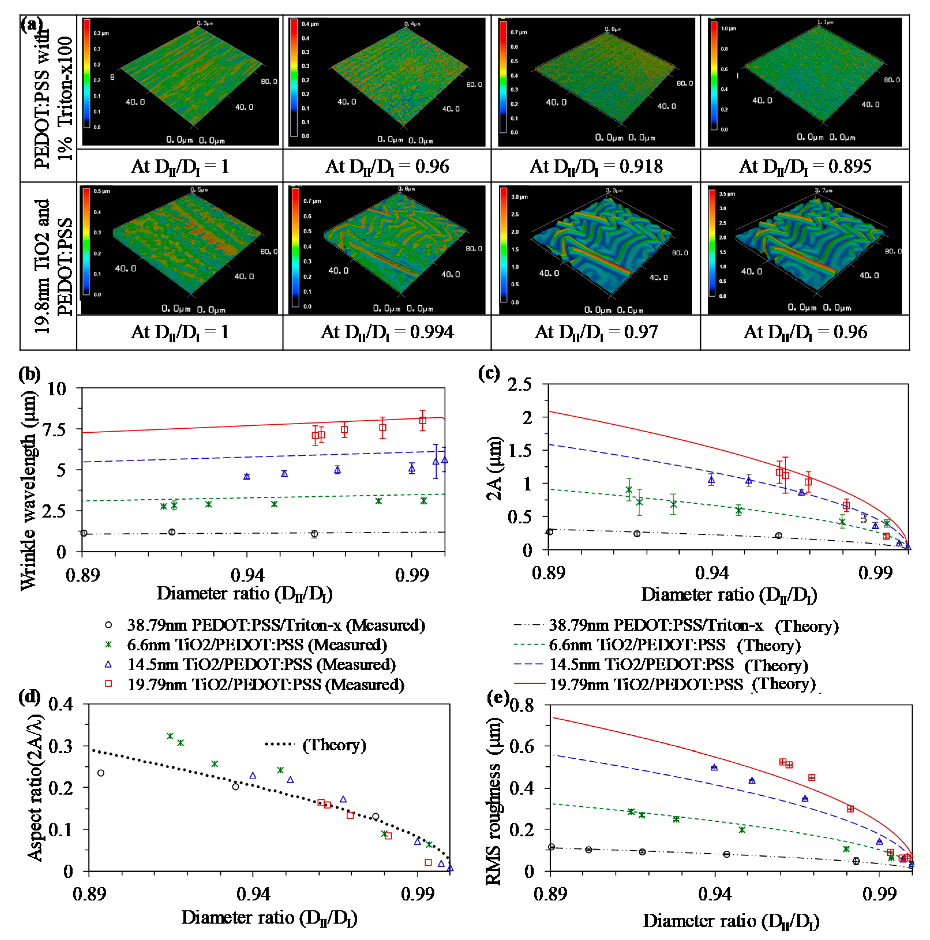
The surface roughness of the PEDOT:PSS/TiO2 coated VHB substrate changes upon formation of the microwrinkles under biaxial compression (e = (DII/DI − 1)). DI is the stress-free diameter which is reduced to DII by the compression strain. The wrinkle topographies depend on the amount of radial compression, the coatings’ elastic modulus (Yf) and thickness (tf) following the Equations (S.18)–(S.20). Therefore, various thin-film thicknesses have been evaluated to visualize their effect in the wrinkle formation and optical scattering. Two types of coating are under investigation, namely (1) a single coating of 38.79 nm thick PEDOT:PSS (with 1% surfactant Triton X-100) on a VHB substrate (Triton X-100 was added as surfactant to coat aqueous PEDOT:PSS ink on hydrophobic VHB substrate), and (2) multilayer coating with the addition of a TiO2 interface between a PEDOT:PSS (pristine with no Triton X-100) coating and VHB substrate. Addition of a TiO2 interface between the PEDOT:PSS and VHB make a stiffer multilayer coating. The thicker the TiO2 interface is, the stiffer this multilayer of PEDOT:PSS/TiO2 is. Three thicknesses of the TiO2 interface were under investigation, namely 6.6 nm, 14.5 nm, and 19.79 nm (as deposited by e-beam evaporation with deposition thickness controlled by time and validated by Dektak 3ST Surface profilometer).
At the stress-free state, the coated surface of PEDOT:PSS/TiO2/VHB is smooth with submicron roughness (see Figure 3a). When subjected to radial compression strain, the surface undulates and forms harmonic or herringbone wrinkles. As the surface roughness is proportional to the wrinkled amplitude (Root Mean Square (RMS) roughness σ = A/√2) for a herringbone surface profile), the radial compression provides a mean to control the surface roughness. Its evolution with the progression of compression strain is like that of wrinkle amplitude (see Figure 3e). An increase of radial compression increases the amplitude at a decreasing rate but linearly reduces the pitch. The measured amplitude and pitch of wrinkles show good agreement with the theoretical model in Equations (S.18)–(S.20). Hence, for these post-buckled wrinkles, the ratio of amplitude to pitch is solely dependent on radial compression but independent of the film property. This agrees well with the theory.
Given a radial compression, the amplitude and pitch of the post-buckled wrinkles depend on the film modulus and thickness. For example, a soft coating of the 38.79 nm thick coating of PEDOT:PSS (with 1% Triton X-100) form only fine wrinkle (250 nm amplitude and an approximately 1 μm pitch) under a large radial compression of 10.6% (i.e., DII/DI = 0.894). In comparison, post-buckling of a stiffer multilayer coating under compression results in a rougher wrinkle surface. Interestingly, only a small radial compression of 4% (i.e., DII/DI = 0.96) is adequate to induce microwrinkles (1.3 μm amplitude and an 8 μm pitch) to a stiffer multilayer coating of 38.79 nm PEDOT:PSS/19.79 nm TiO2. In comparison, a softer multilayer coating with thinner TiO2 interface forms milder wrinkles and roughness under the same compression (see Figure 3c,e). The softer multilayer coating requires a higher compression strain to achieve the same roughness as the stiffer coating does.
These results show that larger surface roughness can be obtained even at lower compression strain by using a coating of larger thickness and elastic modulus. However, the wrinkle slope indicated by the wrinkle aspect ratio (A/λ) is solely dependent on the biaxial compression strain. The implication of this finding on optical scattering will be discussed in the subsequent section.
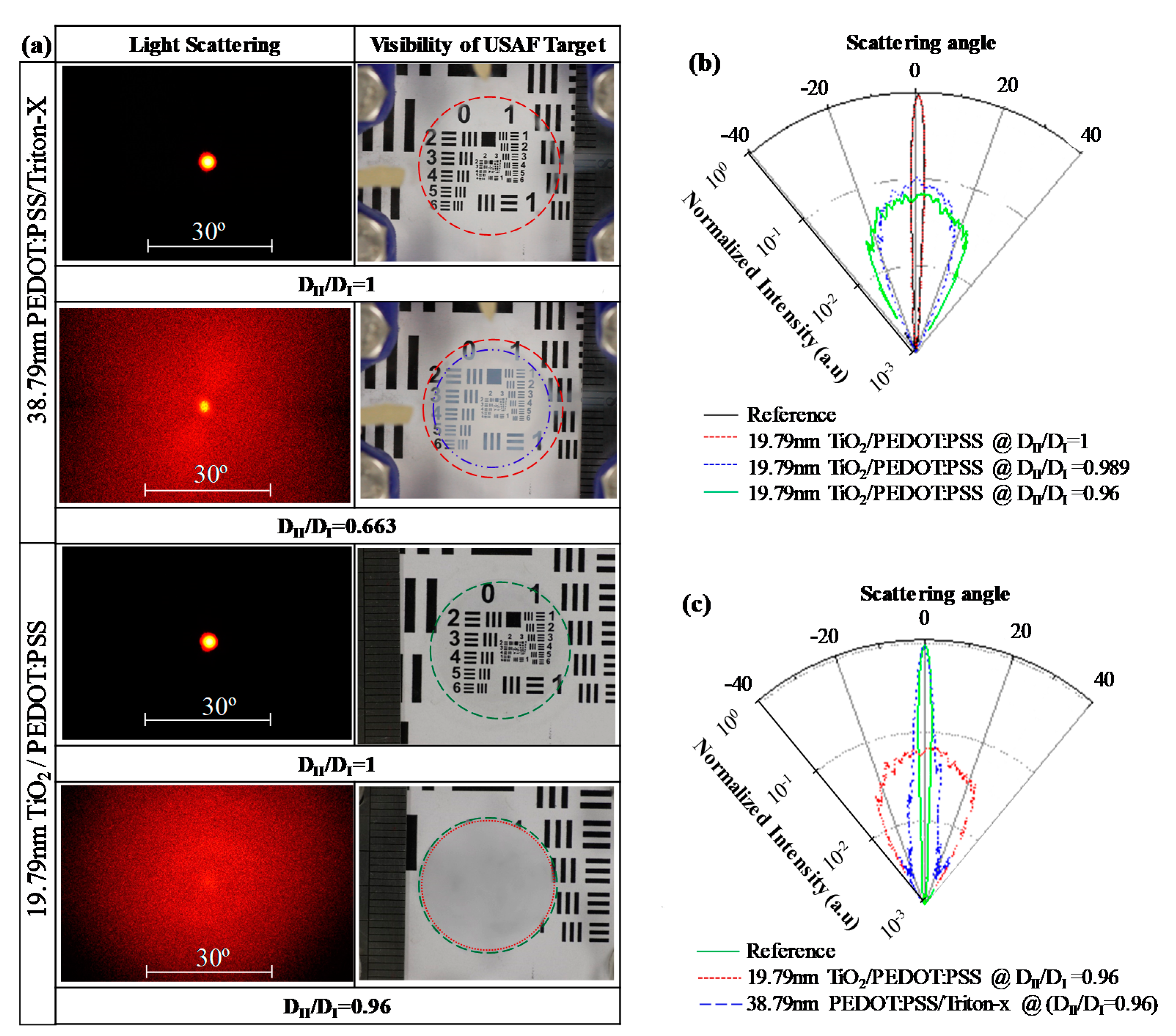
4.1.2. Scattering of Light for Transparency Tuning
A conformable coating of PEDOT:PSS and TiO2 are highly transparent when its surface is smooth at the unwrinkled state (i.e., DII/DI = 1) with merely nanometric roughness. This smooth surface with nanometric roughnesses does not scatter light; full-width half maximum (FWHM) scatter angle of a collimated red laser beam transmitted through the device at DII/DI = 1 is less than 2°. Hence, a USAF target placed 10 mm underneath it is clearly visible (see Figure 4a). When these devices are wrinkled under a radial compression, the initially transparent device becomes translucent. When the radial compression is increased, they appear opaque. Interestingly, a device with thicker TiO2 coats requires lower radial compression strain to reach the opaque state (see Figure 5d). The microwrinkled devices with 19.79 nm TiO2 coats can scatter the transmitted light at a wide angle of 44.77° (FWHM) under a 4% radial compression and are measured to have 1.8% in-line transmittance. A USAF target placed 10 mm beneath this device is completely concealed. Meanwhile, devices with 14.45 nm TiO2 coats require 6–7% radial compression to achieve a similar translucent state.
In comparison, a coating of PEDOT:PSS with 1% Triton X-100 on VHB shows poorer tunability for optical transmittance, as the surface roughness hardly changes even under large radial compression (see Figure 3). The surface of this soft coating remains nearly smooth and transparent under a 4% radial compression. Figure 5d shows that this device requires a very large radial compression of 33% to form noticeable wrinkles (with an amplitude of merely 200–300 μm) which can reduce the inline transmittance to 7.5%. These experimental results are in close agreement with our theoretical analysis.
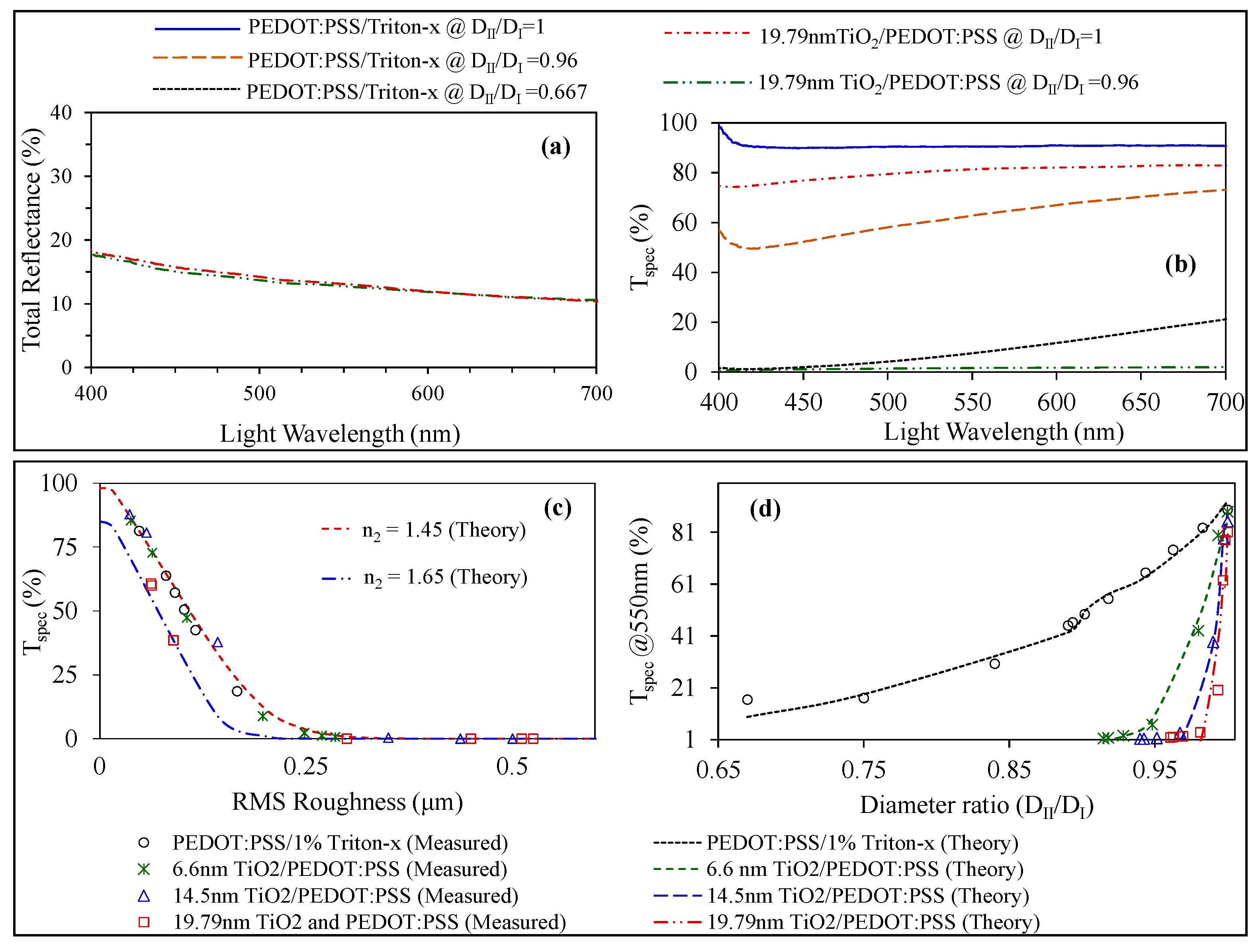
Figure 5c,d shows the upper limit of the optical transparency is limited by the TiO2 film thickness. For instance, the device with 38.79 nm PEDOT:PSS/6.6 nm TiO2 allow specular transmission of 80–90%. Thicker coats of TiO2 are less transparent and more reflective. For example, the double-side coated device with 38.79 nm PEDOT:PSS/14.5 nm TiO2 achieves a maximum inline transmittance of up to 86.5% at the flat states. In comparison, the device coated with 38.79 nm PEDOT:PSS and thicker TiO2 of 19.59 nm achieves a lower maximum inline transmittance of 81.0%. Moreover, a device with only PEDOT:PSS coat is more than 90% transparent.
Figure 5a shows this device is purely an optical diffuser and its total reflectance does not change with the surface unfolding. Figure 5b shows the broadband effect of tunable light scattering. Figure 5c shows that inline transmittance of these optical diffusers is solely dependent on the surface roughness and refractive index of the substrate. As predicted, with an increase in roughness the inline transmittance is lowered at a decreasing rate. Meanwhile, a larger refractive index of the device achieves a larger shift in transmittance. Note that the refractive index mentioned here is the effective refractive index of the combined coating and the substrate. The high refractive index of the TiO2 films increased the effective refractive index of the system making them more effective optical diffuser. Figure 3e shows that a low-strain compression can also introduce adequate micro-wrinkling to a stiffer optical coating and thus switch to a translucent state (see Figure 4a). This low-strain (radial compression ~4%) and high transparency tuning range (81–1.8% inline transmittance for 550 nm light) is demonstrated by a device with a stiffer coated of 19.79 nm TiO2 thin films.
4.1.3. Electrically Tuning the Transparency
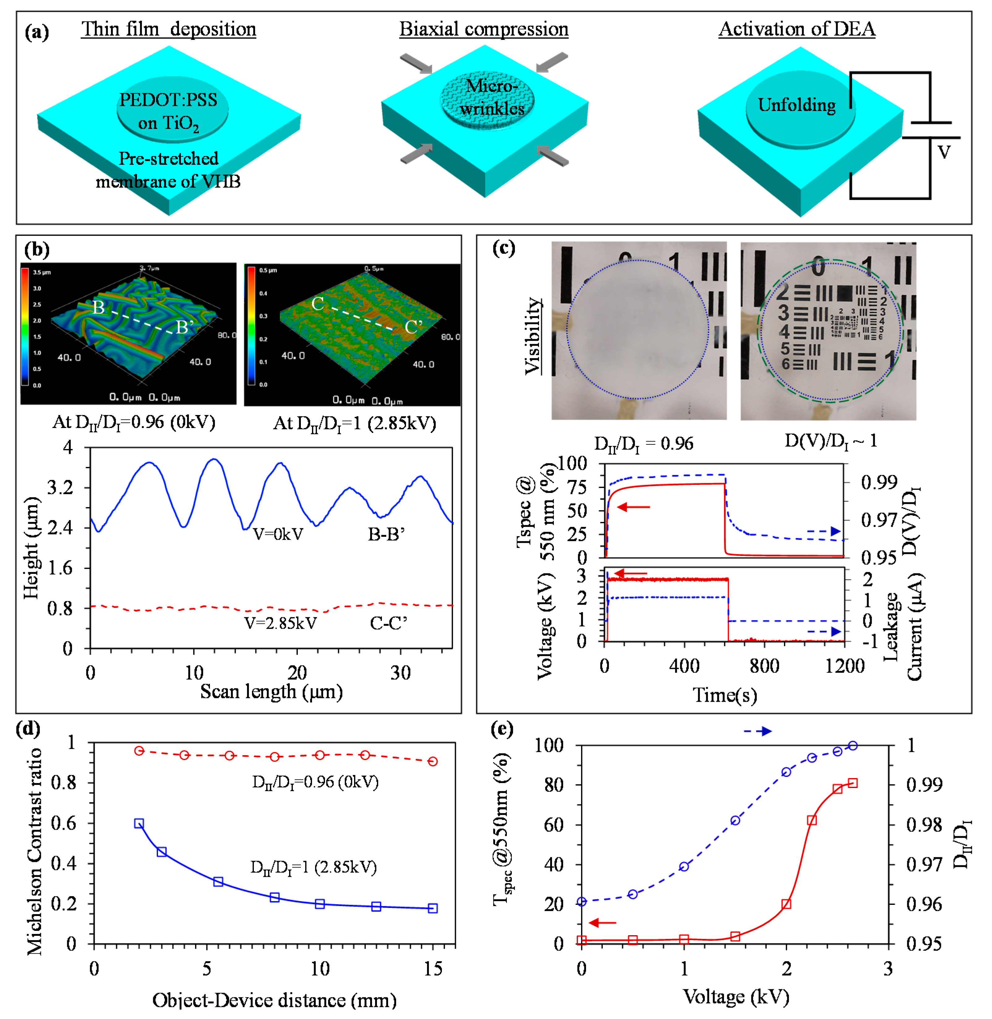
A dielectric elastomer actuator (DEA) provides a means to electrically unfold the wrinkled compliant electrodes. High voltage activation induces a Maxwell stress across the pre-strained membrane of DEA and, in turn, reduces the membrane prestress. This results in an areal expansion over the electrodes and thus useful to unfold and flatten the electrode morphology (refer Figure 6a).
TiO2 interfaces stiffen the nanometric multilayer electrodes and may impede the electrode compression. A DEA with a stiffer interface requires more release of pre-stretch to obtain the same amount of radial compression. Hence, due to lower pre-tension, a higher voltage might be needed to achieve the same voltage-induced areal expansion. The voltage requirement is 2.85 kV for 4% unfolding of the wrinkled compliant electrodes with 19.79 nm TiO2. In comparison, the voltage requirement is low at 2.4 kV for 6% unfolding the wrinkled compliant electrodes with 14.45 nm TiO2. Details of the electrical unfolding for a 20 mm circular device will be elaborated in the subsequent section.
Consider the DEA sandwiched by two electrodes of 38.79 nm thick PEDOT:PSS/19.79 nm TiO2). The electrodes are wrinkled by subjecting to a 4% pre-compressive strain (i.e., DII/DI = 0.96) (see Figure 6b). This capacitive device initially appears ‘opaque’ and it conceals the logo beneath it (see Figure 6c). The time response of switching is obtained by activating the device with an on-off square pulse (10 min each at on (V = 2.85 kV) and off (V = 0 kV)). Figure 6c shows the continuous monitor of diameter expansion of the circular electrode and in-line transmittance during the activation and deactivation. The voltage-induced area expansion of the DEA unfolds the wrinkled metasurface, making it transparent (78–81% transmittance for the green light of 550 nm wavelength). Deactivation of the DEA restores its pre-compression (DII/DI = 0.96), making the meta-surfaces microwrinkled and translucent again (i.e., at 1.85–3.0% in-line transmittance).
In Figure 6c the device was activated for 10 min and then deactivated. Based on the diameter ratio and transmittance plot, the response speed of the voltage-induced areal expansion and corresponding optical switching is evaluated. It takes 44 s to rise to 90% of its steady diameter state while the passive restoration is slower, taking 254 s. This slow response to deactivation is due to the viscoelastic nature of foam tape. Interestingly, the optical switching responses faster. The switching to transparent (i.e., unfolding of the wrinkled surface) takes 60 s (rise time) and the return to opacity (i.e., wrinkling back) takes merely 2 s. This peculiar optical switching response is related to the exponential nature of the relationship between surface roughness and the radial compression (refer Figure 3f). The surface roughness is less sensitive to higher axial compressive strains. Hence, at small compression strain, for example, 0–2% the increment of the roughness is more drastic, hence the transmittance also drops faster. This explains the fast response while switching to opacity despite it’s slower response to reach its original pre-compression state.
The DEA can obtain intermediate transparency states as well. Figure 6e show the activation of the DEA by a stepwise voltage ramp with a voltage step of 0.5 kV and a step time of the 60 s up to 2.65 kV. As the voltage is gradually increased, intermediate areal expansion of DEA is obtained until full pre-compression of wrinkled compliant electrodes is lost at 2.65 kV. The transmittance of the device changes simultaneously and a different state of transmittance is obtained until it becomes completely transparent to its original state. As VHB membrane is a non-ideal dielectric medium, an electrical current will leak through it when it is activated with a high voltage. The electrical power consumption of this device is the product of this applied voltage and the leakage current. This device consumes 0.83 W/m2 at the fully transparent state (see Figure 6c).
Visibility through a diffuser also depends on the distance between the object and the diffuser. Figure 6d shows high visibility with close-to-1 contrast ratio at the on state, but low visibility at the off-state. The transparent state is less sensitive to the device to object distance. But, the contrast ratio at the off state is sensitive to the logo-to-device distance: for example, at the 2 mm gap, the Michelson contrast ratio of the logo viewed through the device is 0.6 but the contrast ratio is merely 0.2 at a 10 mm gap. However, as the gap is increased beyond 15 mm, the visibility through the device is less or not sensitive to the gaps.
4.2. Tunable Acoustic Absorber
Inkjet printing of the PEDOT:PSS thin film as electrodes for the MPDEA simplifies its fabrication process. Besides, the use of transparent electrode makes them applicable for smart windows. Figure 7a shows one of the transparent 2-layer MPDEA with printed PEDOT:PSS electrodes. They are slightly bluish yet optically clear with approximately 80% optical transmittance throughout the visible spectrum (see Figure 7b). The pristine aqueous PEDOT:PSS ink was reformulated by adding Triton X-100 surfactant to improve its wettability to the VHB elastomeric substrate. The reformulated ink is optimized for electrical conductivity and consisted of 40.78 wt.% of PEDOT:PSS, 4.5 wt.% of Triton X-100 and 54.72 wt.% of water. In addition, the spacing of printed droplets was optimized to form a continuous electrode coat. Eventually, 15 μm drop spacing is chosen to print electrodes for the MPDEAs.
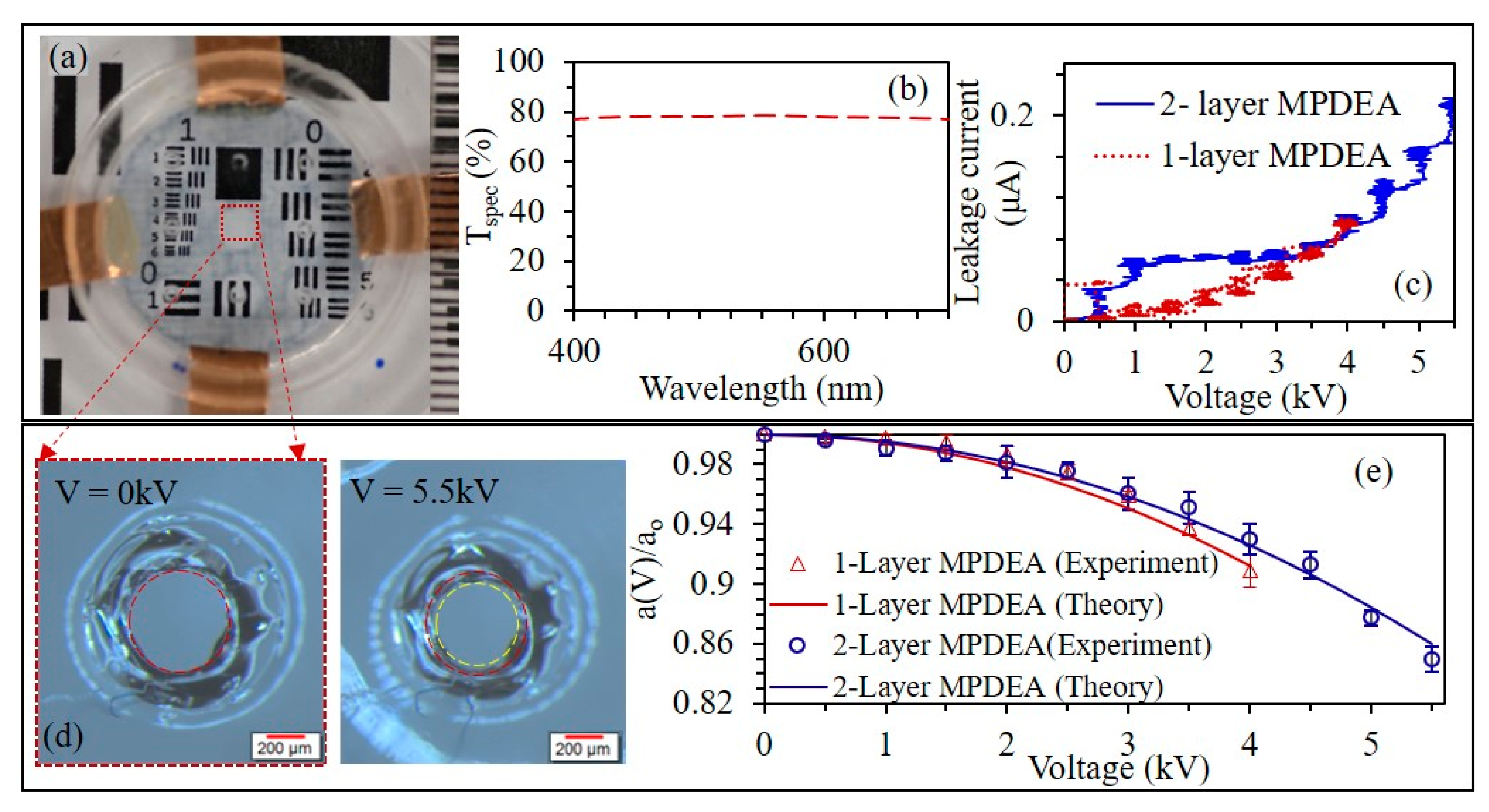
MPDEAs with single and two layers of VHB are investigated. Figure 7d shows electrically obtained change in perforation diameter for both MPDEAs. The electrodes of a 1-layer MPDEA are exposed to air. Hence, the dielectric breakdown of the air occurs above an applied voltage of 4 kV through the holes. However, after self-clearing of PEDOT:PSS layers, they could be activated even up to 5 kV. Meanwhile, the positive electrode of a two-layered MPDEA is isolated from air. It could be activated to a voltage above 5.5 kV and reduce the hole diameter by more than 15%.
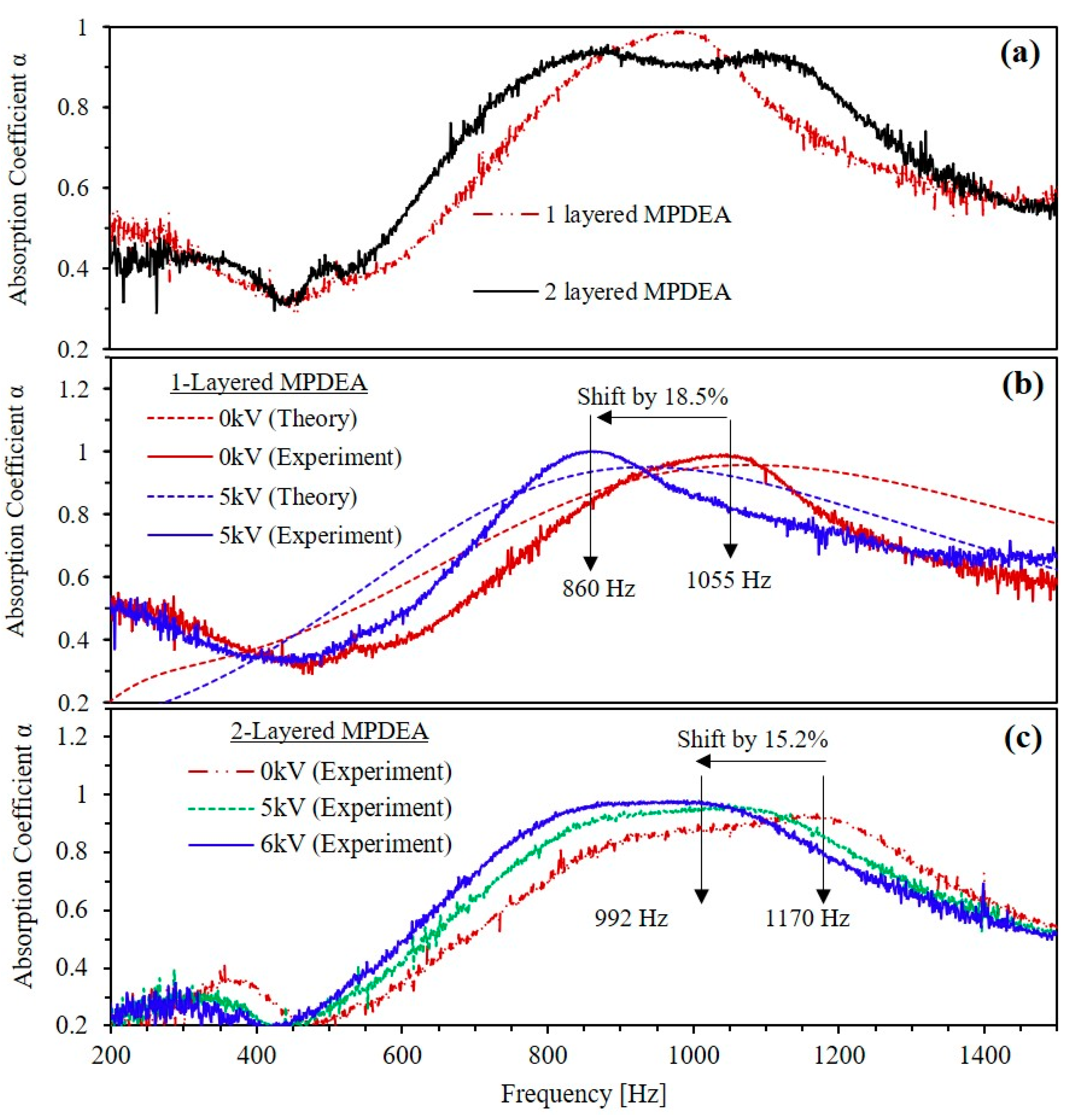
Figure 8a shows the 2-layered MPDEA has relatively broader absorption spectrum compared to the 1-layer MPDEA. The 1-layered MPDEA was activated to shift the absorption spectrum. The electrical activation of the MPDEAs reduced the perforation hole from an inactivated diameter 2ao to a smaller activated diameter 2a(V). The 1-layered MPDEA with 2ao = 447.5 ± 30.78 μm can be driven up to 4 kV to reduce the hole diameter by 10%. It consumes 1.27 watt/m2 electrical power at the activated state. Meanwhile, the 2-layered MPDEA with 2ao = 541.0 ± 25.39 μm when driven at 5.5 kV, it reduces the hole diameter by 15%. Figure 8b shows the experimental and analytical absorption spectrum of 1-layered MPDEA-based tunable acoustic absorbers. In the inactivated state, the bandwidth for above 0.8 acoustic absorption coefficient is 349 Hz (from 831 Hz to 1180 Hz). The peak absorption happens at 1055 Hz at the inactive state (0 kV) but shifts by 18.5% to 860 Hz upon 5.0 kV activation. The theoretical plots are based on Equations (S.23)–(S.24). These plots also show a trend of shifting absorption spectrum upon voltage activation. Figure 8c shows that for the 2-layered MPDEA in the inactive state, the bandwidth for above the 0.8 acoustic absorption coefficient is 444 Hz (from 846–1290 Hz). The peak absorption happens at 1070 Hz at off state (0 kV) but shifted by 15.2% to 992 Hz upon 6.0 kV activation. Figure 7c shows the current leaking through the 1-layered MPDEA at the activated state and based on this plot, this device can consume up to 1.27 W/m2 electrical power.
The transparency tuning unit and the sound-absorbing unit can be combined in parallel with a small gap between the two DEA layers (see Figure 1a). Taken together, this device will consume nearly ~2W/m2 of electrical power when activated. The acoustic and optical performance will be similar to that presented in each individual sections above. Although VHB-based transparency tuning windows are reliable, the sound-absorbing units are less reliable due to micro-perforations in the stretched membrane. Over a long period, such membranes may spontaneously rupture. Some DEAs configured as unimorphs or those that exploit strain in the thickness direction may not require pre-stretching. A sound-absorbing unit based on such DEAs may be of interest to researchers from a reliability and mass production perspective.
5. Conclusions
This work presented a multi-layered solution for tunable optical and acoustic window based on dielectric elastomer actuators and transparent wrinklable compliant electrodes. The first layer is for transparency tuning and its surface roughness is varied employing surface micro-wrinkling or unfolding. As small strain-induced microwrinkling and unfolding is wished to make smart glasses, this work showed microwrinkling of nanometric films of TiO2 of high refractive index are effective to diffuse light down to 1–2% inline transmittance (very frosted) upon less than 5% axial compressive strain. Interestingly, these brittle oxide thin films can sustain thousands of cyclic microwrinkling and unfolding. A conductive overcoat on the oxide film made of the conductive polymer provides electrical conductivity. Such multilayer thin film can make microwrinkled compliant electrode suitable for activating DEA and thus generates voltage induced unfolding. Moreover, this device also showed prominent improvements in terms of power consumption (consumes merely ~0.831 W/m2).
The sound-absorbing layer based on micro-perforated dielectric elastomer actuator can absorb mid-frequency sound while being optically clear (up to 78.64% light transmission). The need for tuning the resonant frequency to match the noise dominant frequency can only be addressed using an MPDEA. We devised a mechanism of tuning hole-diameter by activation of an MPDEA. Unlike other actuators such as an electric motor or mechanical switches, MPDEA provides a distributed and quiet actuation. Such novel smart windows can be made as cheap as glass due to its simple all-solid-state construction. They can be arranged in an array for large area mounting to the window glass. Advances of such transparent tunable acoustic absorbers are anticipated to bring good quality acoustics and natural lighting to the indoor space.
Supplementary Materials
The following are available online at https://0-www-mdpi-com.brum.beds.ac.uk/2076-0825/10/1/16/s1, Video S1: Transparency Tuning, Video S2: Tuning Acoustic Absorption Spectrum, and Supplementary text.
Author Contributions
M.S., Z.L., A.A. and G.-K.L. conceived the idea and designed the study. M.S. contributed to all the material design and device fabrication. M.S. and Z.L. designed the experimental setup and conducted the acoustic testing. M.S., Z.L., and G.-K.L. carried out the data analysis. M.S., Z.L. and G.-K.L. derived the models. M.S. wrote the manuscript. All the authors discussed the results and revised the manuscript. All authors have read and agreed to the published version of the manuscript.
Funding
This research received no external funding.
Institutional Review Board Statement
Not applicable.
Informed Consent Statement
Not applicable.
Data Availability Statement
Data is contained within the article or supplementary material.
Acknowledgments
The first and second authors M.S. and Z.L. was supported by Temasek Foundation Ecosperity Clg Limited, under the grant number TFE1819-NUS-01. The author G.K.L. acknowledged the support by the Ministry of Science and Technology of Taiwan (Grant No. 108-2218-E-009-058-MY3).
Conflicts of Interest
The authors declare no competing financial interest.
References
- Cox, T.J.; D’antonio, P. Acoustic Absorbers and Diffusers: Theory, Design and Application; CRC Press: London, UK; New York, NY, USA, 2009. [Google Scholar]
- Gerriets-GmbH. Absorber Light. Available online: https://www.gerriets.com/us/absorber-light-8172 (accessed on 1 December 2018).
- Lampert, C.M. Chromogenic smart materials. Mater. Today 2004, 7, 28–35. [Google Scholar] [CrossRef]
- Granqvist, C.G. Electrochromics for smart windows: Oxide-based thin films and devices. Thin Solid Films 2014, 564, 1–38. [Google Scholar] [CrossRef]
- Doane, J.W.; Vaz, N.A.; Wu, B.G.; Žumer, S. Field controlled light scattering from nematic microdroplets. Appl. Phys. Letters 1986, 48, 269–271. [Google Scholar] [CrossRef]
- Drzaic, P.S. Polymer dispersed nematic liquid crystal for large area displays and light valves. J. Appl. Phys. 1986, 60, 2142–2148. [Google Scholar] [CrossRef]
- Baetens, R.; Jelle, B.P.; Gustavsen, A. Properties, requirements and possibilities of smart windows for dynamic daylight and solar energy control in buildings: A state-of-the-art review. Solar Energy Mater. Solar Cells 2010, 94, 87–105. [Google Scholar] [CrossRef] [Green Version]
- Zang, J.; Ryu, S.; Pugno, N.; Wang, Q.; Tu, Q.; Buehler, M.J.; Zhao, X. Multifunctionality and control of the crumpling and unfolding of large-area graphene. Nat. Mater. 2013, 12, 321–325. [Google Scholar] [CrossRef] [Green Version]
- Ong, H.-Y.; Shrestha, M.; Lau, G.-K. Microscopically crumpled indium-tin-oxide thin films as compliant electrodes with tunable transmittance. Appl. Phys. Lett. 2015, 107, 132902. [Google Scholar] [CrossRef]
- Van den Ende, D.; Kamminga, J.D.; Boersma, A.; Andritsch, T.; Steeneken, P.G. Voltage-controlled surface wrinkling of elastomeric coatings. Adv. Mater. 2013, 25, 3438–3442. [Google Scholar] [CrossRef]
- Görrn, P.; Cao, W.; Wagner, S. Isotropically stretchable gold conductors on elastomeric substrates. Soft Matter. 2011, 7, 7177. [Google Scholar] [CrossRef]
- Thomas, A.V.; Andow, B.C.; Suresh, S.; Eksik, O.; Yin, J.; Dyson, A.H.; Koratkar, N. Controlled crumpling of graphene oxide films for tunable optical transmittance. Adv. Mater. 2015, 27, 3256–3265. [Google Scholar] [CrossRef]
- Kang, J. An acoustic window system with optimum ventilation and daylighting performance. Noise Vib. Worldw. 2006, 37, 9–17. [Google Scholar] [CrossRef]
- Asdrubali, F.; Pispola, G. Properties of transparent sound-absorbing panels for use in noise barriers. J. Acoust. Soc. Am. 2007, 121, 214–221. [Google Scholar] [CrossRef]
- Struiksma, A.; Tenpierik, M.; Snijder, A.; Veer, F.; Botterman, B.; Hornikx, M.; van der Water, H.; Migchielsen, F. Sound absorbing glass: Transparent solution for poor acoustics of monumental spaces. SPOOL 2017, 4, 53–58. [Google Scholar]
- Soundproofing-Windows.net. Soundproofing Windows with Double and Triple Glazing. Available online: http://soundproofing-windows.net/index.php/soundproofing-windows-with-double-and-triple-glazing (accessed on 1 December 2018).
- Shrestha, M.; Lau, G.-K. Tunable window device based on micro-wrinkling of nanometric zinc-oxide thin film on elastomer. Optics Lett. 2016, 41, 4433. [Google Scholar] [CrossRef]
- Shrestha, M.; Asundi, A.; Lau, G.-K. Smart Window Based on Electric Unfolding of Microwrinkled TiO2 Nanometric Films. ACS Photonics 2018, 5. [Google Scholar] [CrossRef]
- Beckmann, P.; Spizzichino, A. The Scattering of Electromagnetic Waves from Rough Surfaces; Artech House, Inc.: Norwood, MA, USA, 1987; 511p. [Google Scholar]
- Eastman, J. Surface Scattering in Optical Interference Coatings; University of Rochester: New York, NY, USA, 1974. [Google Scholar]
- Zeman, M.; van Swaaij, R.A.C.M.M.; Metselaar, J.W.; Schropp, R.E.I. Optical modeling of a-Si:H solar cells with rough interfaces: Effect of back contact and interface roughness. J. Appl. Phys. 2000, 88, 6436–6443. [Google Scholar] [CrossRef]
- Keplinger, C.; Sun, J.-Y.; Foo, C.C.; Rothemund, P.; Whitesides, G.M.; Suo, Z. Stretchable, transparent, ionic conductors. Science 2013, 341, 984–987. [Google Scholar] [CrossRef] [Green Version]
- Lang, U.; Naujoks, N.; Dual, J. Mechanical characterization of PEDOT:PSS thin films. Synth. Met. 2009, 159, 473–479. [Google Scholar] [CrossRef]
- Lau, G.-K.; Heng, K.-R.; Ahmed, A.S.; Shrestha, M. Dielectric elastomer fingers for versatile grasping and nimble pinching. Appl. Phys. Lett. 2017, 110, 182906. [Google Scholar] [CrossRef]
- Lu, Z.; Shrestha, M.; Lau, G.-K. Electrically tunable and broader-band sound absorption by using micro-perforated dielectric elastomer actuator. Appl. Phys. Lett. 2017, 110, 182901. [Google Scholar] [CrossRef]
- Shrestha, M.; Lu, Z.; Lau, G.-K. Transparent tunable acoustic absorber membrane using inkjet printed PEDOT: PSS thin-film compliant electrodes. ACS Appl. Mater. Interfaces 2018, 10. [Google Scholar] [CrossRef] [PubMed]
- Shrestha, M. Smart window for tuning transparency and noise absorption. Ph.D. Thesis, Nanyang Technological University, Singapore, 2019. [Google Scholar]
- Shrestha, M.; Lu, Z.; Lau, G.K. Ink-jet Printing of Transparent and Stretchable Electrodes for Dielectric Elastomer Actuator. In Proceedings of the 3rd International Conference on Progress in Additive Manufacturing (Pro-AM 2018), Singapore, 14–17 May 2018; pp. 673–678. [Google Scholar] [CrossRef]
- Maa, D.-Y. Potential of microperforated panel absorber. J. Acoust. Soc. Am. 1998, 104.5, 2861–2866. [Google Scholar] [CrossRef]
- Herrin, D.; Liu, J. Properties and applications of microperforated panels. Sound Vib. 2011, 45, 6–9. [Google Scholar]
- Ginn, K. Architectural Acoustics; Brüel & Kjaer: Nærum, Denmark, 1978. [Google Scholar]
- Shian, S.; Clarke, D.R. Electrically tunable window device. Opt. Lett. 2016, 41, 1289–1292. [Google Scholar] [CrossRef]
- Rosset, S.; Shea, H.R. Flexible and stretchable electrodes for dielectric elastomer actuators. Appl. Phys. A 2012, 110, 281–307. [Google Scholar] [CrossRef] [Green Version]
- Li, C.; Cazzolato, B.; Zander, A. Acoustic impedance of micro perforated membranes: Velocity continuity condition at the perforation boundary. J. Acoust. Soc. Am. 2016, 139, 93–103. [Google Scholar] [CrossRef] [Green Version]
- Low, S.H.; Lau, G.K. Bi-axially crumpled silver thin-film electrodes for dielectric elastomer actuators. Smart Mater. Struct. 2014, 23, 125021. [Google Scholar] [CrossRef]
Figure 1.
(a) Schematic of the smart window made of two components, first component can tune its transparency and second can absorb noise while adapting to the varying noise frequency; Schematic of the transparency tuning device based on dielectric elastomer actuator (DEA) optical scatterer (b) optically scattering state at inactive state; (c) optically transparent state at activated state. (d) Schematic of the microperforated dielectric elastomer actuator (MPDEA) device; (e) magnified view of a hole of the MPDEA at the inactive state; (f) a hole of the MPDEA at activated state.

Figure 2.
Fabrication procedure of the (a) transparency tuning device; (b) tunable acoustic absorber; measurement setup at various activation voltage for (c) optical inline transmittance measurement; (d) normal acoustic absorption.
Figure 2.
Fabrication procedure of the (a) transparency tuning device; (b) tunable acoustic absorber; measurement setup at various activation voltage for (c) optical inline transmittance measurement; (d) normal acoustic absorption.

Figure 3.
Increase in the wrinkle wavelength and amplitude with the addition of TiO2 to the poly(3,4-ethylenedioxythiophene) polystyrene sulfonate (PEDOT:PSS) layer. (a) Confocal images showing as-deposited and wrinkled states with the progression of the wrinkle formation; plots of wrinkle’s (b) wavelength, (c) amplitude, (d) aspect ratio and (e) root mean square (RMS) roughness vs. electrode diameter ratio at increasing compression strain; the theoretical results are based on Equations (S.18)–(S.20).

Figure 4.
Scattering of normally incident laser beam and corresponding transparency of the devices: (a) image of laser spot through an unwrinkled device which is later scattered through the wrinkled surface; (b) angular light intensity distribution by the 19.79 nm TiO2 and 38.79 nm PEDOT:PSS coated devices at different compression strain; (c) comparison of angular light intensity distribution between 19.79 nm TiO2/PEDOT:PSS and just PEDOT:PSS coated devices at same compression strain of 4%.

Figure 5.
(a) Total reflectance of the TiO2/PEDOT:PSS films at flat and wrinkled states; (b) comparison of inline transmission throughout visible spectrum for the devices with coats of PEDOT:PSS and TiO2/PEDOT:PSS at different compression strain. The trend of reduction in inline transmission with increasing: (c) RMS roughness validated experimentally and theoretically; (d) with increasing radial compression for different TiO2 thickness (theoretical results are based on Equation (1) validated with the experimental results).

Figure 6.
Voltage-controlled unfolding of a microwrinkled surface of the DEA-based transparency tuning device (coating layers of 39.79 nm PEDOT:PSS and 19.79 nm TiO2). (a) Schematic showing formation of microwrinkles and change in device area and the surface upon voltage activation; (b) 3D confocal images and 2D profile of the same device at different active and inactive states; (c) corresponding appearance of a USAF target placed 10 mm beneath the device, its on-off time response in terms of inline transmittance and electrode diameter change and corresponding voltage and current; (d) change Michelson contrast ratio of the USAF target placed at varying distance from the device at On and Off states; (e) gradual change in inline transmittance (Tspec) induced by an electrically obtained change in compression states (DII/DI).

Figure 7.
(a) A prototype of the two-layered transparent MPDEA device with inkjet-printed PEDOT:PSS thin film electrode; (b) inline transmittance of the same device for the visible spectrum. When it is electrically activated, the active area expands, and the hole diameter shrinks: (c) the applied voltage and the leakage current of the 1 and 2-layer MPDEAs; (d) one of the holes at passive (0 kV) and activated state (5.5 kV); (e) plot showing a gradual reduction in the hole diameter when the activation voltage is gradually increased (theoretical plots are based on Equation (3)).

Figure 8.
(a) Comparison of the acoustic absorption spectrum of a single and double-layered absorber with printed PEDOT:PSS electrodes; tuning of the acoustic absorption spectrum by voltage activation using: (b) 1-layered MPDEA absorber (theoretical plots are based on Equations (S.23)–(S.28) and parameters given in Supplementary text Section 3.0) and (c) 2-layered MPDEA absorber.

Publisher’s Note: MDPI stays neutral with regard to jurisdictional claims in published maps and institutional affiliations. |
© 2021 by the authors. Licensee MDPI, Basel, Switzerland. This article is an open access article distributed under the terms and conditions of the Creative Commons Attribution (CC BY) license (http://creativecommons.org/licenses/by/4.0/).
Share and Cite
MDPI and ACS Style
Shrestha, M.; Lau, G.-K.; Asundi, A.; Lu, Z. Dielectric Elastomer Actuator-Based Multifunctional Smart Window for Transparency Tuning and Noise Absorption. Actuators 2021, 10, 16. https://0-doi-org.brum.beds.ac.uk/10.3390/act10010016
AMA Style
Shrestha M, Lau G-K, Asundi A, Lu Z. Dielectric Elastomer Actuator-Based Multifunctional Smart Window for Transparency Tuning and Noise Absorption. Actuators. 2021; 10(1):16. https://0-doi-org.brum.beds.ac.uk/10.3390/act10010016
Chicago/Turabian StyleShrestha, Milan, Gih-Keong Lau, Anand Asundi, and Zhenbo Lu. 2021. "Dielectric Elastomer Actuator-Based Multifunctional Smart Window for Transparency Tuning and Noise Absorption" Actuators 10, no. 1: 16. https://0-doi-org.brum.beds.ac.uk/10.3390/act10010016
Note that from the first issue of 2016, this journal uses article numbers instead of page numbers. See further details here.