Article

Facile Solution Synthesis, Processing and Characterization of n- and p-Type Binary and Ternary Bi–Sb Tellurides

1
Department of Applied Physics, KTH Royal Institute of Technology, SE10691 Stockholm, Sweden
2
Department of Physics, Istanbul University, Fatih, Istanbul 34320, Turkey
3
Department of Inorganic Materials, Slovak University of Technology in Bratislava, 812 37 Bratislava, Slovak Republic
4
Department of Elec. and Elec. Engineering, Istanbul University-Cerrahpasa, Avcilar, Istanbul 34135, Turkey
5
Department of Materials and Environmental Chemistry, Stockholm University, SE-106 91 Stockholm, Sweden
6
ŁUKASIEWICZ Research Network—PORT Polish Center for Technology Development, Stablowicka 147, 54-066 Wroclaw, Poland
7
Institute of Experimental Physics, University of Wroclaw, Maxa Borna 9, 50-204 Wroclaw, Poland
*
Author to whom correspondence should be addressed.
Submission received: 11 December 2019 / Revised: 26 January 2020 / Accepted: 3 February 2020 / Published: 10 February 2020

Abstract

:

Featured Application

This article presents a truly scalable, energy and cost-effective, and reproducible solution chemical synthesis method for thermoelectric materials.

Abstract

The solution synthesis route as a scalable bottom-up synthetic method possesses significant advantages for synthesizing nanostructured bulk thermoelectric (TE) materials with improved performance. Tuning the composition of the materials directly in the solution, without needing any further processing, is important for adjusting the dominant carrier type. Here, we report a very rapid (2 min) and high yield (>8 g/batch) synthetic method using microwave-assisted heating, for the controlled growth of Bi2–xSbxTe3 (x: 0–2) nanoplatelets. Resultant materials exhibit a high crystallinity and phase purity, as characterized by XRD, and platelet morphology, as revealed by SEM. Surface chemistry of as-made materials showed a mixture of metallic and oxide phases, as evidenced by XPS. Zeta-potential analysis exhibited a systematic change of isoelectric point as a function of the material composition. As-made materials were directly sintered into pellets by using spark plasma sintering process. TE performance of Bi2−xSbxTe3 pellets were studied, where the highest ZT values of 1.04 (at 440 K) for Bi2Te3 and 1.37 (at 523 K) for Sb2Te3 were obtained, as n- and p-type TE materials. The presented microwave-assisted synthesis method is energy effective, a truly scalable and reproducible method, paving the way for large scale production and implementation of towards large-area TE applications.

Graphical Abstract

1. Introduction

Metal chalcogenide-based materials are commonly good thermoelectric (TE) materials with a high thermoelectric figure of merit. Bismuth telluride (Bi2Te3) and its alloys ((BiSb)2(SeTe)3) are currently the most promising TE materials in bulk form, at ambient temperature region, due to their high figure of merit in comparison to other material [1]. The dimensionless figure of merit is defined as ZT = (S2σT)/κ, where S is the Seebeck coefficient, σ is the electronic conductivity, T is the temperature, and κ is the total thermal conductivity. Theoretical analysis and experimental explorations suggest that low dimensional materials such as nanostructures, quantum wells, quantum wires, and quantum dots should have much higher thermoelectric performance than their bulk counterparts [2,3,4]. The highest ZT value, for Bi2Te3 based materials, thus far (∼2.4) has been obtained in Bi2Te3/Sb2Te3 superlattices [5]; however, the outstanding ZT values were not reproduced, nor is the material scalable for implementing in large-scale applications. Based on the theoretical predictions, one-dimensional nanostructures including nanowires and nanotubes could reach high ZT values (>5) [6], which has not been realized yet.
A review on the synthesis of Bi2Te3 nanostructures has been recently reported elsewhere [7]. Bi2Te3 is normally synthesized by fusion of bismuth (Bi) and tellurium (Te) metals forming an ingot, or by powder metallurgy [8]. Arc melting, a high energy process, has been shown to be a fast and reproducible synthetic method for high performance Bi2−xSbxTe3 structures [9,10], even combined with solidification under magnetic field, yielding textured materials [11]. Bi2Te3 nanostructures with various morphologies such as nanoparticles [12,13,14], nanosheets [15,16], films [17], nanowires [18], hollow nanospheres [14], nanorods [19,20], and nanotubes [21,22] have been prepared by various routes, including solvothermal [23] or hydrothermal method, polyol method [13], electrodeposition [19,20], etc. Among these methods, solvothermal or hydrothermal reaction processes are performed in autoclaves and usually require long reaction time (in the order of many hours to days). Electrodeposition of nanowires/nanorods require custom-made templates with special pore structure, which will dictate the resultant particle morphology. Some of these techniques are either very energy intensive or time consuming, still limiting the bulk production of these materials for niche applications. Therefore, developing a more convenient and rapid way for the bulk scale synthesis of Bi2Te3 nanostructures and its alloys is still needed. Solution chemical methods may be advantageous for the synthesis of these materials at large scale if energy effective and highly reproducible synthetic methods can be developed, which may be troubling especially when the produced volumes are large.
Microwave (MW) heating has been demonstrated to be a feasible method for the synthesis of TE nanomaterials directly in the solution phase. It has been shown to make it possible to perform reactions that have been done in several hours to days in a fraction of the time using MW-assisted heating, which is very energy effective, causing an effective and rapid volume heating, avoiding the thermal fluctuations in conventional heating, creating particles with more or less similar particle size. This type of a process is also important in the field of TEs in order to systematically investigate the influence of initial particle size and morphology in the resultant microstructure and TE transport characteristics of the materials. There are few reports on the MW-assisted method for the synthesis Bi2Te3. Harpeness et al. attempted to synthesize Bi2Te3 by MW-assisted polyol method [24], where they obtained Bi3Te4 instead of Bi2Te3. The synthesis of Bi2Te3 nanorods and nanoflakes in ethylene glycol by MW heating method has been reported [25] where the reaction duration ranged from 0.5 h to 6 h. Jiang et al. [14] synthesized hollow Bi2Te3 nanospheres at 150 °C through the MW-assisted heating method. They also reported on hollow spheres, nanosaws, and sheets [26]. Qin et al. presented a MW-assisted heating route for Bi2Te3 nanosheets and nanotubes using ethylene glycol as the solvent with a synthesis duration from 0.5 to 1 h. They demonstrated that the morphology of the resultant structure was strongly dependent on the reaction conditions, forming only nanosheets at low temperature (180 °C), transforming to nanotubes at high temperature (195 °C) [26]. Pradhan et al. reported on the MW-assisted synthesis of spherical Bi2Te3 nanoparticles from a homogeneous solution of tartarate complex of Bi3+ and Te4+ in a reaction time of 10 min [27].
Despite the recent developments in the synthesis of thermoelectric Bi2Te3 nanostructures using the MW-assisted heating, only one of the above listed works reported on transport properties of the fabricated materials [27], leaving a gap from the synthesis to application. This could be mainly due to the quantity of material synthesized per batch being rather limited, as can be assessed from the experimental details (concentrations and volumes of the precursors used; see Table S1 for overview of the literature on MW-assisted synthesis of Bi2Te3). It is also well-known that consolidation process, and the resultant microstructure, is critical for the final performance of the thermoelectric materials. Here, we present on the MW-assisted synthesis of Bi2−xSbxTe3 nanoparticles from a homogeneous solution of ethylene glycol and chloride salts of Bi and Sb, while Te is complexed with TOP/TBP, producing high purity thermoelectric nanopowders in a matter of minutes due to very effective volume heating. Besides yielding large quantity (>8 g) of the investigated materials per batch, the processing of these materials towards compacts is described, resulting in high ZT values of 1.04 for Bi2Te3 and 1.37 for Sb2Te3 as n- and p-type materials, respectively.

2. Materials and Methods

2.1. Synthesis and Processing of Thermoelectric Nanopowders

The following chemicals were used for the synthesis reaction: BiCl3 (Sigma Aldrich, Sweden, 98%), SbCl3 (Sigma Aldrich, Sweden, 99.95%), Te powder (Sigma Aldrich, Sweden, 99.8%), ethylene glycol (EG; Sigma Aldrich, Sweden, 99%), thioglycolic acid (TGA; Sigma Aldrich, Sweden, 98%), tri-butyl phosphine (TBP; Sigma Aldrich, Sweden, 93.5%), and tri-octyl phosphine (TOP; Sigma Aldrich, Sweden, 90%). All chemicals were used as received, without further purification.
The synthesis work was performed via MW-assisted thermolysis (flexiWAVE–Milestone, 1800 Watt; equipped with multivessel high pressure rotor) reaction inside a 100 mL Teflon vessel, in 4 parallel reaction vessels at a single run. The synthesis process starts with the preparation of precursor solutions. In the first step, Te precursor solution was prepared as a complex with TBP (or TOP) by heating a mixture of 0.96 g of Te in 6 mL TBP (or 10 mL TOP) under MW field for about 90 s at 220 °C under constant stirring, and then left to cool down. For the Bi (or Sb) precursor, 1.6 g of BiCl3 was dissolved in 20 mL ethylene glycol. The stoichiometry of ternary compositions can easily be tuned by replacing the BiCl3 precursor with equivalent moles of SbCl3. A 1-mL aliquot of TGA as a directing agent was added to the dissolved precursors, and then sonicated to obtain a homogeneous solution. The two prepared solutions of Te-TOP complex and Bi/Sb - EG were mixed and added to a 100 mL Teflon vessel and run in the MW reactor for 2 min dwell time at 220 °C under constant stirring. The product (dark powder), which is about 2 g per vessel, was then cooled down to room temperature. The as-prepared Bi2−xSbxTe3 phases were separated clearly from the solvent (EG). The multivessel high pressure rotor was used for the MW synthesis work (Figure S1), where only four of the fifteen reactor positions were more than enough to prepare large quantity (>8 g) of the desired materials in a single run. Particles were easily separated from the reaction mixture by centrifuging and washing with iso-propanol and acetone several times. A typical outcome of separation process is shown in Figure S2.

2.2. Consolidation of Thermoelectric Nanopowders Using Spark Plasma Sintering (SPS)

The powders were consolidated using the spark plasma sintering SPS with 15 mm inner diameter graphite cylinders with top and bottom punches made as well from graphite. All powders were processed with the same parameter during the SPS process to obtain pellets with similar porosity in terms of the thermoelectric transport properties of the Bi2−xSbxTe3 compositions. The SPS temperature was set to 400 °C with a heating rate of 30 °C /min and 1-min dwell time. Then, 50 MPa Pressure was applied gradually during the SPS process. The holding time was set to 1 min for both applied current and pressure. Finally, the pellet was cooled from 400 °C to 250 °C, while the load was decreased from 50 MPa to 0 MPa. The pellets were then removed from the die and polished in three steps to remove the contaminated surface by the graphite punches and to obtain smooth surface with 1 μm roughness for further processing and analysis. Table 1 summarizes the pressing parameters and the density of the resultant pellets.

2.3. Structural and Morphological Characterization

X-ray Powder Diffraction (XRPD) was used to identify the crystalline phase of the nanoparticles on a PANalytical X’Pert PRO, equipped with a Copper anode (Cu–Kα1 radiation) with a step size of 0.24° in continuous mode and a scan speed of 0.04 °/s. The crystalline phases of the Bi2−xSbxTe3 system was determined by using Rietveld refinement using High-score pro program. Scanning electron microscopy (SEM; FEI Nova 200) was used for studying the microstructure and morphology of the materials.
X-ray photoelectron spectroscopy (XPS) was used, where the XPS spectra were acquired using PREVAC 426 system configuration, equipped with SCIENTA R3000 hemispherical photoelectron spectrometer and monochromatic Al Kα source operating at 450 W. The base pressure in the analysis chamber was better than 3 × 10⁻¹⁰ mbar. All acquired spectra were calibrated to adventitious carbon C1s at 285 eV. The overall resolution of the spectrometer during measurements was 0.65 eV as a full width of half maximum (FWHM) of the Ag3d5/2 line. After subtraction of the Shirley-type background, the core-level spectra were decomposed into main components with mixed Gaussian–Lorentzian lines (70% G + 30% L for majority of photo-peaks) by a non-linear least squares curve-fitting procedure, using CasaXPS software. XPSPeak software was also used for deconvolution, which allows for the flexible deconvolution parameter changes.
The ξ -potential of various samples were measured at room temperature with Zetasizer Nano ZS90 at an incident angle of 90°. All samples were diluted in DI H2O and titrated with 0.1 M HCl or 0.1 M NaOH to obtain pH dependent surface charge, and eventually determine the isoelectric point (iep). The measurements were performed in triplicate.

2.4. Transport Property Evaluation

The Seebeck coefficient S and the electrical conductivity σ were measured simultaneously on the pellets obtained after the SPS process using a commercial instrument ZEM-ULVAC M8 model. This system measures the S and σ based on the four-probe point method. Typical error in both electrical conductivity and Seebeck coefficient measurements is estimated as 4% in total. The total thermal conductivity κ was calculated using the specific heat capacity Cp, thermal diffusivity α, and density ρ using the equation κ = Cp α ρ. The density of the samples could be obtained from Archimedes method, while a laser flash analysis system (LFA 1000, Linseis) was used for obtaining the thermal diffusivity α. Differential scanning calorimetry (Netzsch-DSC 404 Pegasus214 Polyma) was used to measure the specific heat capacity Cp. The thermal range used during the tests was 298–523 K, and with all the properties known the TE figure of merit ZT was estimated.

3. Results and Discussion

Polyol synthesis is a promising route for the synthesis of various metallic nanoparticle systems, where the solvent polyalcohol acts also as the reducing agent for the metallic ions in the solution. Here, the method esd applied for the TE material synthesis, with an important change of using MW-assisted heating for the reaction, which makes it possible to synthesize large quantities of high-quality nanomaterials in a matter of 2–3 min. The mechanism of synthesis consists of two parts, the first one being the reduction of Bi3+/Sb3+ ions to metallic Bi/Sb by the solvent EG, which in turn catalyzes the breaking of the bond between Te and TOP (Te(TOP)), forming directly the crystalline Bi2−xSbxTe3 phase without needing any further thermal treatment. The overall reaction taking place during the formation of Bi2−xSbxTe3 compounds under MW irradiation can be represented as follows:
Bi3+/Sb3+ + ethyleneglycol → Bi/Sb + EG(ox),
(2 − x) Bi + x Sb + 3 Te(TOP) → Bi2−xSbxTe3 + 3 TOPO,
where EG(ox) refers to the formation of diacetyl molecules due to the oxidation of EG during the reduction of metallic ions of Bi3+/Sb3+ into corresponding metallic particles (see Figure S3 for molecular structure of TOP and EG as well as their oxidation products). Thermodynamic properties of binary chalcogenide compounds were reported previously by Semenkovich et al. [28], where their Gibbs free energies (ΔG) of formation were experimentally estimated at various temperatures. The ΔG values are negative for pure Bi2Te3 (−19.30 ± 0.07 kcal/mol @ 503K) and Sb2Te3 (−15.4 ± 0.3 kcal/mol @ 540 K), revealing the feasibility and spontaneity of their formation under the reaction conditions (493 K). Chemical analysis was performed using ICP and elemental ratio, as expected from the initial precursor concentration, has been confirmed for the Bi2−xSbxTe3 materials.

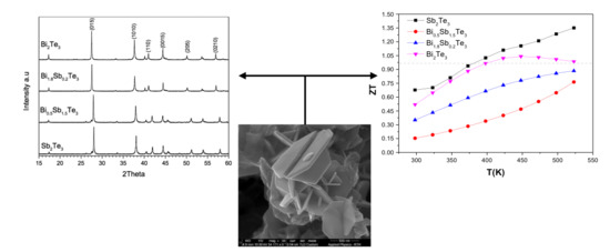
3.1. Structural Analysis

Structural analyses of as-synthesized materials and sintered pellets were performed using XRPD and the diffraction patterns are presented in Figure 1. The phases are indexed to Bi2Te3 (ICDD: 01-082-0358) and Sb2Te3 (ICDD: 01-071-0393) with rhombohedral crystal structure, and the corresponding indexing is designated on the powder diffraction patterns in Figure 1a. No impurity peaks are observed, revealing the high purity of the as-made materials. Due to the similarity of reduction potential of Bi3+ and Sb3+ ions, step-wise transformation of the synthetic chemistry from pure Bi2Te3 to pure Sb2Te3 phase was very smoothly handled at the reaction temperature. The shift of the position for the major peak indexed to (015), going from Bi2Te3 to Sb2Te3, can be observed in Figure 1b, which is ascribed to systematic shrinkage of the Bi2Te3 lattice by the introduction of Sb, as Sb2Te3 has slightly smaller lattice dimensions (a = b = 4.395 Å for Bi2Te3 and 4.264 Å for Sb2Te3, crystal structure, as displayed in Figure S4a). Based on the lattice parameters the shrinkage in a and b corresponds to about 3% by increasing x (in Bi2−xSbxTe3) from 0 to 2, while going from Bi2Te3 to Sb2Te3 following Vegard’s rule (see Figure S4). The width of the diffraction peaks with the same index vary from sample to sample, which is ascribed to the small crystallite size and non-uniform strain within the materials. XRPD analyses performed on the sintered samples showed narrower diffraction peaks, variation of peak intensities from powder samples, due to the crystal/grain growth (Figure 1c), and reduced strain within the material upon exposure to high T and pressure for a brief period.

3.2. Morphology and Surface Analysis

SEM micrographs of Bi2−xSbxTe3 samples at different magnifications are presented in Figure 2. All samples show particles with clear hexagonal, or truncated-edge hexagonal, platelet morphology, in agreement with their rhombohedral layered crystal structure, with slight change of platelet size from one sample to another. In some cases, various platelets sharing a common axis are observed. Lateral size of hexagonal platelets varies in the range from 50 to 500 nm for different samples, where the thickness is typically around 50 nm. Sb2Te3 sample display the largest lateral size of hexagonal platelets up to about 1 μm, which aligns with its high crystallinity and narrower peak width observed in XRPD. A closer investigation of platelets performed by using TEM for the Bi2Te3 sample, as an example, revealed crystalline domains (see Figure S5). There is a thin disordered layer on the nanoplatelets (see Figure S5b) which may be due to residual carbon materials or slightly different, disordered lattice.
The synthetic method and the solvents used significantly influences surface chemistry of resultant materials. In the polyol synthesis, nanoparticles may have residual chemicals on the surface, which may influence their dispersion, sintering, or some other processing characteristics. Therefore, XPS analysis was performed on the as-made materials and the resultant spectra for Bi 4f, Sb 3d, and Te 3d regions are presented in Figure S6. Carbon residue is present on all samples with varying degrees. XPS peak fitting results are summarized in Table 1, disregarding the C and O content. For all samples, during the deconvolution process, oxide phases were identified. For Sb3d and Te3d regions, metallic and oxide phases were clearly visible. In the case of Bi4f region, high resolution spectra allowed determining metallic and oxide (Bi2O3) phases. The most remarkable outcome is the evidence on the presence of oxide phases on the surface of as-made nanoplatelets.
Zeta potential ( ξ -potential) analysis is a technique for determining the surface charge of nanoparticles in solution in colloidal form. Nanoparticles possess a surface charge that attracts a thin layer of ions of opposite charge to their surface, and when the surface charge is balanced by the attracted oppositely charged ions, the total surface charge becomes zero. This point is defined as the isoelectric point (iep) and is strongly dependent on the surface exposed species. ξ -potential is usually studied as a function of an additive, most commonly as a function of pH in the solution—where pH is adjusted by the step-wise addition of acid or base solution into the colloidal system. Study of iep of the as-synthesized Bi2−xSbxTe3 materials as a function of pH is, therefore, expected to reveal the surface chemistry of as-made nanoplatelets. While all materials showed residual carbon, which should be the same type of organics due to the synthesis process used, the surface chemistry showed great variations in zeta potential analysis. Dependence of the pH at the iep on the Sb content, x, for Bi2−xSbxTe3 samples is presented in Table 1. For the pure Bi2Te3 (x = 0), the iep was reached at pH 6.3, which shifts step-wise down to 3.3 with the increasing content of Sb (x > 0). A survey of iep for various oxides led to the values of 2.9 for Sb2O3 and 8.2 for Bi2O3, while no data were found for TeO2 [29]. We performed zeta potential analysis on commercial TeO2 powder and obtained an iep value of 5.2. XPS data, as summarized in Table 1, suggest similar TeO2 content for the samples Bi2Te3 and Sb2Te3, while the other oxide phases (Bi2O3 and Sb2O3) vary in quantity depending on the x. The ternary phases revealed iep values in between those of samples where 2 > x > 0. This agrees with the trend that would be expected in parallel to the changes in Bi2O3 or Sb2O3 content. When x = 0, the surface shows a closer character to Bi2O3 with an iep of around 6.5, which is lower than pure Bi2O3 due to the co-existence of TeO2. This value changes towards more acidic region with the increasing x (Sb content), reaching the iep of 3.3 at x = 2, a bit higher than Sb2O3 due to the co-presence of TeO2. Although these data are not deterministic, they help to get a better insight into the nanoplatelets’ surface in connection with the XPS results.

3.3. Transport Property Evaluation

Nanostructured TE materials were consolidated using SPS, the critical consolidation parameters (sintering temperature, holding time, pressure, and heating rates), and characteristics of the resultant pellets are presented in detail in Table 2. All pellets possess a compaction density of about 78–83% of the theoretical density of the material, with about 20% porosity. The transport data in the temperature range 300–523 K are presented in Figure 3a–e. Table 2 also summarizes the transport data at room temperature and at the temperature where maximum ZT was obtained for the given material composition. No adverse effects in the transport properties were observed due to the presence of surface oxides. The Seebeck coefficient (S) is the key parameter to demonstrate that the materials have the transport characteristics (n- vs. p-type) planned for from the stoichiometry of the precursors. Figure 3a reveals the sign and magnitude of measured S values, which clearly indicates n-type character for Bi2Te3 and Bi1.8Sb0.2Te3, while p-type character was observed for Bi0.5Sb1.5Te3 and Sb2Te3. This, in agreement with literature, is a strong indication that the MW-assisted chemical synthesis process is capable of producing the phases that are designated by the initial ratio of precursor materials, without needing additional stabilizers, reflux, or other chemicals to avoid phase separation during synthesis. An interesting comparison for the obtained S could be for Bi0.5Sb1.5Te3 composition with arc-melted and textured (via solidification under magnetic field) material [11], where our S value is about two times lower. Electronic transport properties are strongly correlated in classical materials, as well as by charge carrier density, defects, and scattering events. Therefore, it is possible to observe different transport values in the same composition due to the microstructure, which in turn is mostly determined by the synthesis and processing methods. The textured material possessed larger micro- to nano-sized grains, or layers, causing strong scattering of charge carriers and heat carrier phonons (decrease electronic and thermal conductivity), which in turn enhanced the S. SEM and TEM micrographs of our samples prepared with solution chemical process showed small nano-sized, nearly identical crystalline nanoplatelets. This microstructure allows decoupling of thermal conductivity from the electronic transport by increased density of grain boundaries, thus increased scattering of phonons (mainly reducing the lattice component of the thermal conductivity). The combined overall positive effects were seen in the details of electronic and thermal transport properties, as presented below.
The electrical conductivity (σ) is plotted in Figure 3b, where samples show either very minor change or slight reduction of σ by increasing temperature, which is typical of heavily doped semiconductors, or metallic character. The highest electrical conductivity values were measured for Sb2Te3 and Bi1.8Sb0.2Te3 samples. The electrical conductivity of our two n-type and one p-type Bi2−xSbxTe3 samples are higher than those of other solution derived samples [23,31,32] and comparable with that of p-type alloy ingot (on the level of 1 × 10³ S/cm at 300 K) [33]. The lower electrical conductivity of Bi2Te3 in comparison to Sb2Te3 arises from the intrinsically small band gap, Eg, of this compound (~0.13 eV) [34]. Given such a small Eg, the minority carriers are more easily thermally excited, and the resulting detrimental bipolar effect also introduces extra thermal conductivity. Therefore, to increase the electrical conductivity of Bi2Te3, the Eg has to be widened/broadened. The Eg of Sb2Te3 is ~0.28 eV [35], and Sb doping in Bi2Te3 helps to optimize the carrier concentration and introduces strong point defect scattering of heat-carrying phonons. However, there is an inherent restriction of Sb doping: doping with too high a content of Sb will lead to too great a hole concentration because of the reduced formation energy of antisite defects, resulting in a reduced κ and an increased κe [36]. This is the main reason that Bi1.5Sb0.5Te3 shows both higher electrical and thermal conductivity. Similarly, Bi doping in Sb2Te3 reduces the electrical conductivity likely due to decreased energy band gap and increased number of thermally activated minority carriers. As a result, doping with either Bi or Sb in Bi–Sb–Te compounds finely tunes the key electrical parameters such as the valley degeneracy, carrier concentration, effective mass, deformation potential, and band gap [37,38].
The power factor (PF) (S2 σ) was calculated for all samples, as presented in Figure 3c. The highest PF values were obtained for the pure phase samples of Bi2Te3 and Sb2Te3, followed by Bi1.8Sb0.2Te3 and Bi0.5Sb1.5Te3. The magnitude of PF is comparable to or higher than that of earlier reports: the maximum power factor at 300 K we achieved are 20.35 μW cm−1 K2 for Bi2Te3 and 21.94 μW cm−1 K2 for Sb2Te3 pellet, which are much higher than other solution-derived samples—with maximum power factor 1–9 μW cm−1 K2 [27,31].
Thermal conductivity (κ) values were calculated from the thermal diffusivity, density, and Cp values. The trend is a decrease in κ by increasing temperature, while the values at room temperature (RT) range from about 0.9 to 1.2 W/mK. The sample with the composition Bi2Te3 showed a decreasing trend of κ, which increased slightly after 400 K. This was attributed to bipolar effect, likely due to lower Eg, thus thermally activated minority carriers in this compound. Zhang et al. reported κ values in the range of 0.9–2.4 W/mK at RT for solvothermally synthesized nanoplatelets of BixSb2−xTe3 [23]. Our values are similar to, or slightly lower than, their results and even that of bulk ingot Bi2Te3 (1.5 W m−1 K−1). Thermal conductivity has two contributors: electronic (κel) and lattice (κlat) components. Nanostructuring is known to reduce the thermal conductivity of the material by phonon scattering, which influences the κlat mainly. κel can be estimated using Wiedemann–Franz law, by calculating the electronic contribution (κel) to the κ and thereafter κlat can be obtained subtracting κel from the total κ (κtot). The Lorenz number (Lo) for all compounds was calculated by using the following equations:
L   =   ( k B e ) 2 [ ( r + 7 / 2 ) F r + 5 / 2 ( ξ ) ( r + 3 / 2 ) F r + 1 / 2 ( ξ ) ( ( r + 5 / 2 ) F r + 3 / 2 ( ξ ) ( r + 3 / 2 ) F r + 1 / 2 ( ξ ) ) 2 ]
where r is the scattering parameter, kB the Boltzmann constant, e is the electron charge, and Fn (ξ) is the Fermi integral given by
F n ( ξ ) = 0 χ n 1 + e χ ξ d χ
Here, ξ is the reduced Fermi energy that can be calculated from the Seebeck coefficient S and the scattering parameter r according to
S = k B e ( r + 5 / 2 ) F r + 3 2 ( ξ ) ( r + 3 / 2 ) F r + 1 2 ( ξ )     ξ
We used parabolic band model and assumed the system to be highly degenerate and scattering is dominated by acoustic phonons. The calculated Lo numbers, along with the estimated κel and κtot for all samples are displayed in Table S2. Looking at the proportion of the κel, the major part of κtot is dominated by electronic contribution in Bi2Te3 and Bi1.8Sb0.2Te3 samples, while κlat is predominant in thermal conductivity of Sb2Te3 and Bi0.5Sb1.5Te3. This might be due to either phonon-point defect scattering or phonon grain boundary scattering (due to nanosized grains). The negative value of κlat of Sb2Te3 at room temperature is not realistic, which indicates that the parabolic band model may not be suitable for calculating Lo for this sample. In any case, it is important to see how κlat can strongly affect the transport properties and thus play a major role in enhancing the ZT value for these compositions.
Using all these transport parameters, the resultant figure-of-merit, ZT, has been estimated and the results are presented in Figure 3e, where a monotonic increase was observed for all samples by increasing temperature. Pure Bi2Te3 and Sb2Te3 samples show ZT values around 0.5–0.6 at RT, reaching beyond unity around 440 K. From this point onwards, the trend in Sb2Te3 is still linear while that of Bi2Te3 bends downwards, mainly due to the increase in the thermal conductivity due to bipolar effect. Bi2Te3 reached a ZT of 1.04, while Sb2Te3 reached to 1.20 at 440 K. The ternary phases where Bi and Sb are co-doped also showed favorable ZT values by increasing temperature, reaching about 0.75–0.90 at 523 K. The highest ZT of 1.37 is achieved for pure Sb2Te3 sample at 523 K, likely due to its lower thermal conductivity that is suppressed by phonon point defect and phonon grain boundary scattering.
Fine thermoelectric powders as presented here are very valuable resources in the field of large area and flexible hybrid thermoelectric materials research. Many of the published works on hybrids have relied on commercial powders for making their films where micron size Bi2Te3 material is either exfoliated via sonication, or ball-milled to reduce the particle size to prepare a good polymer nanoparticle hybrid. We attempted to show the ease of integration of as-made Bi2Te3 material with PVDF and made few hybrid films using doctor blading method (see Figure S8). Our results show that stable dispersions can be easily made and films with reasonable transport properties can be obtained. A typical output from this film is n-type Seebeck (S = −46.12 μV/K), and electrical conductivity of around 0.6013 S/m leading to a power factor of PF= 1.284 × 10⁻³ μW/mK2 (see Figure S9). This value can be further improved by a careful interface engineering, the choice of the polymer, or changing the ratio of polymer vs. nanoparticle content in the hybrid films, which is one of the major directions of on-going research.

4. Conclusions

Microwave assisted polyol synthesis was used to fabricate high-purity nanostructured Bi2−xSbxTe3 (where x: 0–2) thermoelectric materials in a matter of minutes, in a very highly reproducible manner. Besides dramatically shortening the synthesis time, the quantities that can be fabricated per batch (>8 g) is unprecedented in other solution synthetic techniques. Fabricated materials exhibit hexagonal (or truncated hexagonal) platelet particle morphology in agreement with the rhombohedral crystal structure. Thermoelectric performance of Bi2−xSbxTe3 pellets were studied, where the highest ZT values of 1.04 (at 440 K) for x: 0 (Bi2Te3) and 1.37 (at 523 K) for x: 2 (Sb2Te3) were obtained, respectively, as n- and p-type TE materials. Ternary compositions, where x: 0.2 and 1.5, reached ZT of 0.8–0.9 at 523 K, which are also promising values for thermoelectric conversion. The large density of grain boundaries has been effective in reducing the thermal conductivity of the materials, thus making it possible to achieve ZT values in the order of 1 or above for pure phases of Bi2Te3 and Sb2Te3. Furthermore, due to their small size and favorable surface chemistry, the as-made nanoparticles could easily be used to fabricate hybrid thermoelectric films. The devised MW-assisted synthesis technique, which is energy and resource effective resulting in thermoelectric materials with promising performance, opens avenues for large scale production of heat-energy harvesting materials. In addition, complete thermoelectric devices can be realized by combining our n-type and p-type Bi2−xSbxTe3 materials. Furthermore, the presented method is truly scalable and can be tuned for one-pot synthesis of even quaternary compositions such as (BiSb)2(TeSe)3.

Supplementary Materials

The following are available online at https://0-www-mdpi-com.brum.beds.ac.uk/2076-3417/10/3/1178/s1, Table S1. Literature review on microwave (MW)-assisted synthesis of Bi2Te3. Details of the synthetic route (solvent, reactor), reaction temperature-time; morphology of resultant structures; the quantity typically obtained according to described procedure in the articles; and the reported transport data. Figure S1. (a) Screenshot of the reactor for experimental design using multivessel rotor. (b) Multivessel high pressure rotor used for the MW-assisted synthesis of Bi2−xSbxTe3 nanoparticles. The system can take up to 15 reactors, which can be filled up to about 100 mL each, making it possible to synthesize high and reproducible quality nanostructures with a high yield, at a pilot scale, without needing any complicated or reflux systems. Figure S2. (a) Typical temperature (T)–time (t)–power (P) profile of the MW-assisted synthesis process for Bi2−xSbxTe3 samples. (b) As-synthesized sample transferred to a centrifuge vial and phase separation is easily achieved, yielding typically 2–3 g sample per reactor vessel. Four positions/vials (out of 15) during the MW-assisted reaction is sufficient to prepare 8–10 g of these materials within a reaction time of 2 min. Figure S3. Reaction mechanism showing the molecular structure of organic components used for the polyol synthesis of Bi2−xSbxTe3 nanoparticles. While Bi2−xSbxTe3 nanoparticles are formed, ethyleneglycol (EG) is converted to diacetyl (rxn (1)) and trioctylphosphine (TOP) is converted to trioctylphosphine oxide (TOPO) (rxn (2)). Figure S4. Estimated change of the lattice parameter a (or b) by substitution of Sb (x) in Bi2−xSbxTe3 system. Figure S5. (a) TEM micrograph of a typical as-made Bi2Te3 nanoparticle with a lateral cross-sectional size of about 500 nm; (b) high resolution micrograph showing lattice fringes; and (c) Fourier-transform of the selected square region in (b) showing crystalline nature of Bi2Te3 nanoplatelet. Figure S6. High resolution XPS Spectra of as-made Bi2−xSbxTe3 samples, for the regions Bi 4f, Sb 3d, and Te 3d. Table S2. Transport properties for nanostructured bulk Bi2−xSbxTe3: mass density (άρ) in percentage of the theoretical density, total thermal conductivity (κtot), Lorentz number (Lo), electronic thermal conductivity (κel), and lattice thermal conductivity (κlat). Figure S7. Hybrid thermoelectric film (1.5 × 5 cm2) with Ag paste contact. The films are made by blending the as-made thermoelectric nanoparticles with the polymer PVDF. Figure S8. Microstructure of the as-made Bi2Te3 nanoparticles–PVDF hybrid thermoelectric film at different magnifications. PVDF is visible as a dark shade in the rightmost micrograph, showing perfusing nanoparticles. Figure S9. Device characteristic of the large area film made with Bi2Te3 nanoplatelets and PVDF. The resultant transport qualities for the film are S = −46.12 μV/K, σ = 0.6013 S/m, leading to a power factor of PF = 1.284 × 10⁻³ μW/mK2.

Author Contributions

M.S.T. conceived the presented idea. B.H., V.R., and M.S.T. contributed to conceptualization and methodology, material synthesis, and original draft preparation. B.H., H.B., and M.O. contributed to physicochemical characterization. B.H. and M.O. processed the material. S.B. and A.Y. validated the thermoelectric properties. M.K. and R.S. performed the XPS analysis. All authors discussed the results and reviewed and edited the manuscript. M.S.T. and M.J. supervised the work. All authors have read and agreed to the published version of the manuscript.

Funding

This research was funded by the Swedish Energy Agency (Energimyndigheten, 43521-1) and in part by Swedish Research Agency Council (VR, 2018-03462) as well as EC-H2020 (UncorrelaTEd Grant ID: 863222). SB acknowledges support by Scientific and Technological Research Council of Turkey (TUBITAK, 216M254) and Scientific Research Projects Coordination Unit of Istanbul University (BAP, 21809 and 32641).

Acknowledgments

MST acknowledges the financial support from Olle Engkvist Foundation (SOEB, 190-0315) for the establishment of microwave synthesis facilities.

Conflicts of Interest

The authors declare no conflict of interest.

References

  1. Boyer, A.; Cissé, E. Properties of thin film thermoelectric materials: Application to sensors using the Seebeck effect. Mater. Sci. Eng. B 1992, 13, 103–111. [Google Scholar]
  2. Dresselhaus, M.S.; Dresselhaus, G.; Sun, X.; Zhang, Z.; Cronin, S.B.; Koga, T. Low dimensional thermoelectric materials. Phys. Solid State 1999, 41, 679–682. [Google Scholar] [CrossRef]
  3. Hicks, L.D.; Dresselhaus, M.S. Thermoelectric figure of merit of a one-dimensional conductor. Phys. Rev. B-Condens. Matter Mater. Phys. 1993, 47, 16631–16634. [Google Scholar]
  4. Hicks, L.D.; Dresselhaus, S.M. Effect of quantum-well structures on the thermoelectric figure of merit. Phys. Rev. 1993, 47, 12727–12731. [Google Scholar]
  5. Venkatasubramanian, R.; Siivola, E.; Colpitts, T.; Quinn, B.O. Thin-film thermoelectric devices with high room-temperature figures of merit. Nature 2001, 413, 597–602. [Google Scholar] [CrossRef] [PubMed]
  6. Lin, Y.M.; Sun, X.; Dresselhaus, M. Theoretical investigation of thermoelectric transport properties of cylindrical Bi nanowires. Phys. Rev. B-Condens. Matter Mater. Phys. 2000, 62, 4610–4623. [Google Scholar]
  7. Mamur, H.; Bhuiyan, M.R.A.; Korkmaz, F.; Nil, M. A review on bismuth telluride (Bi2Te3) nanostructure for thermoelectric applications. Renew. Sustain. Energy Rev. 2018, 82, 4159–4169. [Google Scholar] [CrossRef]
  8. Madavali, B.; Kim, H.S.; Lee, K.H.; Isoda, Y.; Gascoin, F.; Hong, S.J. Large scale production of high efficient and robust p-type Bi–Sb–Te based thermoelectric materials by powder metallurgy. Mater. Des. 2016, 112, 485–494. [Google Scholar] [CrossRef]
  9. Serrano-Sánchez, F.; Gharsallah, M.; Nemes, N.M.; Biskup, N.; Varela, M.; Martínez, J.L.; Fernández-Díaz, M.T.; Alonso, J.A. Enhanced figure of merit in nanostructured (Bi,Sb)2Te3 with optimized composition, prepared by a straightforward arc-melting procedure. Sci. Rep. 2017, 7, 1–10. [Google Scholar] [CrossRef] [Green Version]
  10. Gharsallah, M.; Serrano-Sánchez, F.; Bermúdez, J.; Nemes, N.M.; Martínez, J.L.; Elhalouani, F.; Alonso, J.A. Nanostructured Bi2Te3 Prepared by a Straightforward Arc-Melting Method. Nanoscale Res. Lett. 2016, 11, 1–7. [Google Scholar] [CrossRef] [Green Version]
  11. Luo, Y.; Yang, J.; Jiang, Q.; Fu, L.; Xiao, Y.; Li, W.; Zhang, D.; Zhou, Z.; Cheng, Y. Melting and solidification of bismuth antimony telluride under a high magnetic field: A new route to high thermoelectric performance. Nano Energy 2015, 15, 709–718. [Google Scholar] [CrossRef]
  12. Cao, Y.Q.; Zhao, X.B.; Zhu, T.J.; Zhang, X.B.; Tu, J.P. Syntheses and thermoelectric properties of Bi2Te3 Sb2Te3 bulk nanocomposites with laminated nanostructure. Appl. Phys. Lett. 2008, 92, 90–93. [Google Scholar]
  13. Cao, Y.Q.; Zhu, T.J.; Zhao, X.B.; Zhang, X.B.; Tu, J.P. Nanostructuring and improved performance of ternary Bi–Sb–Te thermoelectric materials. Appl. Phys. A Mater. Sci. Process. 2008, 92, 321–324. [Google Scholar]
  14. Jiang, Y.; Zhu, Y.J. Bi2Te3 nanostructures prepared by microwave heating. J. Cryst. Growth 2007, 306, 351–355. [Google Scholar]
  15. Shi, W.; Zhou, L.; Song, S.; Yang, J.; Zhang, H. Hydrothermal synthesis and thermoelectric transport properties of impurity-free antimony telluride hexagonal nanoplates. Adv. Mater. 2008, 20, 1892–1897. [Google Scholar]
  16. Li, S.; Zhang, S.; He, Z.; Toprak, M.; Stiewe, C.; Muhammed, M.; Müller, E. Novel solution route synthesis of low thermal conductivity nanocrystalline bismuth telluride. J. Nanosci. Nanotechnol. 2010, 10, 7658–7662. [Google Scholar] [CrossRef]
  17. Li, S.; Toprak, M.S.; Soliman, H.M.; Zhou, J.; Muhammed, M.; Platzek, D.; Müller, E. Fabrication of nanostructured thermoelectric bismuth telluride thick films by electrochemical deposition. Chem. Mater. 2006, 18, 3627–3633. [Google Scholar]
  18. Yu, H.; Gibbons, P.C.; Buhro, W.E. Bismuth, tellurium, and bismuth telluride nanowires. J. Mater. Chem. 2004, 14, 595–602. [Google Scholar]
  19. Li, S.; Liang, Y.; Qin, J.; Toprak, M.; Muhammed, M. Template electrodeposition of ordered bismuth telluride nanowire arrays. J. Nanosci. Nanotechnol. 2009, 9, 1543–1547. [Google Scholar]
  20. Prieto, A.L.; Sander, M.S.; Martín-González, M.S.; Gronsky, R.; Sands, T.; Stacy, A.M. Electrodeposition of ordered Bi2Te3 nanowire arrays. J. Am. Chem. Soc. 2001, 123, 7160–7161. [Google Scholar]
  21. Xiao, F.; Yoo, B.; Kyu, H.L.; Myung, N.V. Synthesis of Bi2Te3 nanotubes by galvanic displacement. J. Am. Chem. Soc. 2007, 129, 10068–10069. [Google Scholar]
  22. Zhao, X.B.; Ji, X.H.; Zhang, Y.H.; Zhu, T.J.; Tu, J.P.; Zhang, X.B. Bismuth telluride nanotubes and the effects on the thermoelectric properties of nanotube-containing nanocomposites. Appl. Phys. Lett. 2005, 86, 062111. [Google Scholar]
  23. Zhang, C.; Peng, Z.; Li, Z.; Yu, L.; Khor, K.A.; Xiong, Q. Controlled growth of bismuth antimony telluride BixSb2−xTe3 nanoplatelets and their bulk thermoelectric nanocomposites. Nano Energy 2015, 15, 688–696. [Google Scholar]
  24. Harpeness, R.; Gedanken, A. Microwave-assisted synthesis of nanosized Bi2Se3. New J. Chem. 2003, 27, 1191–1193. [Google Scholar] [CrossRef]
  25. Zhou, B.; Zhao, Y.; Pu, L.; Zhu, J. Microwave-assisted synthesis of nanocrystalline Bi2Te3. Mater. Chem. Phys. 2006, 96, 192–196. [Google Scholar]
  26. Yao, Q.; Zhu, Y.; Chen, L.; Sun, Z.; Chen, X. Microwave-assisted synthesis and characterization of Bi2Te3 nanosheets and nanotubes. J. Alloys Compd. 2009, 481, 91–95. [Google Scholar]
  27. Pradhan, S.; Das, R.; Bhar, R.; Bandyopadhyay, R.; Pramanik, P. A simple fast microwave-assisted synthesis of thermoelectric bismuth telluride nanoparticles from homogeneous reaction-mixture. J. Nanoparticle Res. 2017, 69, 19. [Google Scholar]
  28. Semenkovich, S.A.; Melekh, B.T. Thermodynamic Properties of Bi2Te3, Bi2Se3, Sb2Te3 and Sb2Se3. In Chemical Bonds in Solids; Springer: New York, NY, USA, 1972; pp. 159–162. [Google Scholar]
  29. Kosmulski, M. Isoelectric points and points of zero charge of metal (hydr)oxides: 50 years after Parks’ review. Adv. Colloid Interface Sci. 2016, 238, 1–61. [Google Scholar] [CrossRef]
  30. Crist, B.V. Handbook of Monochromatic XPS Spectra—The Elements and Native Oxides; Volume 1 in PDF; XPS International LLC: Mountain View, CA, USA, 1999. [Google Scholar]
  31. Scheele, M.; Oeschler, N.; Veremchuk, I.; Reinsberg, K.G.; Kreuziger, A.M.; Kornowski, A.; Broekaert, J.; Klinke, C.; Weller, H. ZT enhancement in solution-grown Sb(2−x)BixTe3 nanoplatelets. ACS Nano 2010, 4, 4283–4291. [Google Scholar] [CrossRef] [Green Version]
  32. Zhao, Y.; Dyck, J.S.; Hernandez, B.M.; Burda, C. Enhancing thermoelectric performance of ternary nanocrystals through adjusting carrier concentration. J. Am. Chem. Soc. 2010, 132, 4982–4983. [Google Scholar] [CrossRef]
  33. Poudel, B.; Hao, Q.; Ma, Y.; Lan, Y.; Minnich, A.; Yu, B.; Yan, X.; Wang, D.; Muto, A.; Vashaee, D.; et al. High-thermoelectric performance of nanostructured bismuth antimony telluride bulk alloys. Science 2008, 320, 634–638. [Google Scholar] [CrossRef] [PubMed] [Green Version]
  34. Xu, Z.; Wu, H.; Zhu, T.; Fu, C.; Liu, X.; Hu, L.; He, J.; He, J.; Zhao, X. Attaining high mid-Temperature performance in (Bi,Sb)2Te3 thermoelectric materials via synergistic optimization. NPG Asia Mater. 2016, 8, e302. [Google Scholar] [CrossRef]
  35. Sehr, R.; Testardi, L.R. The optical properties of p-type Bi2Te3-Sb2Te3 alloys between 2–15 microns. J. Phys. Chem. Solids 1962, 23, 1219–1224. [Google Scholar] [CrossRef]
  36. Hu, L.P.; Zhu, T.J.; Wang, Y.G.; Xie, H.H.; Xu, Z.J.; Zhao, X.B. Shifting up the optimum figure of merit of p-type bismuth telluride-based thermoelectric materials for power generation by suppressing intrinsic conduction. NPG Asia Mater. 2014, 6, e88. [Google Scholar] [CrossRef] [Green Version]
  37. Charoenphakdee, A.; Yamanaka, S.; Snyder, G.J. Enhancement of Thermoelectric of the Electronic Density of States. Science 2008, 321, 1457–1461. [Google Scholar]
  38. Wang, H.; Gibbs, Z.M.; Takagiwa, Y.; Snyder, G.J. Tuning bands of PbSe for better thermoelectric efficiency. Energy Environ. Sci. 2014, 7, 804–811. [Google Scholar] [CrossRef] [Green Version]
Figure 1. XRD powder patterns of powder Bi2−xSbxTe3 samples: (a) in the 2θ range of 15–60; and (b) 2 θ range of 26–29, focusing on the peak with the miller indices of (015), showing the shift of the peak position towards larger 2θ values due to shrinking lattice by substituting Bi with Sb. (c,d) The XRD patterns of the sintered pellets measured perpendicular to the pressing direction. The crystalline phases are indexed to Bi2Te3 (ICDD: 01-082-0358) (for x = 0) and Sb2Te3 (ICDD: 01-071-0393) (for x = 2) with rhombohedral crystal structure.
Applsci 10 01178 g001
Figure 2. SEM micrographs at different magnifications of as-synthesized: (a,e) Bi2Te3; (b,f) Bi1.8Sb0.2Te3; (c,g) Bi0.5Sb1.5Te3; and (d,h) Sb2Te3.
Applsci 10 01178 g002
Figure 3. The temperature dependent transport properties of the synthesized Bi2−xSbxTe3 samples: (a) Seebeck coefficient, S; (b) electrical conductivity, σ; (c) Power factor; (d) thermal conductivity, κ; and (e) the overall thermoelectric figure of merit, ZT.
Applsci 10 01178 g003
Table 1. XPS peak fitting results for Bi 4f, Sb 3d, and Te 3d regions for bulk samples, and the measured iep values for the Bi2−xSbxTe3 samples.
SamplesBE [eV] [30]FractionAssigned to [31]iep (pH)
Bi2Te315713.11Bi6.3
1599.83Bi–O (Bi2O3)
5738.77Te
57719.68Te–O (TeO2)
Bi1.8 Sb0.2Te31576.06Bi6
528.32.08Sb
5736.5Te
1594.56Bi–O (Bi2O3)
5301.42Sb–O (Sb2O3)
57710.35Te–O (TeO2)
Bi0.5 Sb1.5Te31572.38Bi4.5
528.312.64Sb
57311.46Te
1592.38Bi–O (Bi2O3)
5308.43Sb–O (Sb2O3)
57715.7Te–O (TeO2)
Sb2Te3528.314.92Sb3.3
5738.38Te
5309.94Sb–O (Sb2O3)
57722.13Te–O (TeO2)
Table 2. SPS parameters and transport properties for nanostructured bulk Bi2−xSbxTe3: sintering temperature (Tsint), holding time (thold), sintering pressure (Psint), mass density (ρ) in percentage of the theoretical density, thermal conductivity (κ), Seebeck coefficient (S), electrical conductivity (σ), power factor (PF), and the thermoelectric figure of merit (ZT).
SampleTsint (°C)thold (min)Psint (MPa)ρ %T (K)κ (W m−1 K−1)S (μVK−1)σ−1 m−1)PF (μWK2 cm−1)ZT
Bi2Te3400150783000.94788−124.624106356.5820.350.52
4400.87553−159.46680018.3916.521.04
Bi1.8Sb0.2Te3400150833001.33091−89.190197582.3717.410.35
5231.05234−128.942104707.3415.720.87
Bi0.5Sb1.5Te3400150783000.85478104.87340077.906.810.15
5230.46612157.33927504.004.410.76
Sb2Te3400150813001.11645104.893230549.9121.940.68
5230.84984152.56594246.9525.371.37

