1. Introduction
Electrical resistivity tomography (ERT) is a method for determining the electrical resistivity distribution in a volume from discrete measurements of current and voltage made within a volume or on its surface [
1]. ERT conception was first proposed by Shima [
2] in 1987, and it has been widely used in China since 1990s as a programmable automatic switching controller. Right now, distributed ERT is the most popular. The ERT method is a commonly used geophysical prospecting manner which is widely applied in hydrology, ocean exploration, engineering, and environment geological exploration and investigation [
3,
4]. Single-channel ERT has been used for many years [
5]. Multi-channel ERT was developed in the past twenty years or so but is not so widely employed. It is extremely suitable for super higt density ERT. The ERT in this article refers to a single ERT system. Multi-channel ERT can access all channel data at the same time and can obtain all possible combination tests, therefore it is time saving and has high precision. Simultaneously, it needs more complicated hardware and more fussy inversion calculations. It is normally used in 3D tests with many electrode requests, which may take several hours for one round of testing. Whereas for the ERT applications that do not have too many electrodes, single-channel ERT has widely been employed [
5], e.g., long-time ERT monitoring systems with relatively minimal data requirements [
4,
6].
Substantially, the ERT system consists of the usual electric logging and electrode switching device. Therefore, it is called a super multi-meter. Distributed ERT is the most efficient ERT monitoring method at present. The electrode switching device (ESD) is an important component of ERT, and it is also a key differentiator between ERT and conventional electrical resistivity. A monitoring instrument has been developed along with the electronic technique. The development of ESD, to a great extent, affects the future of ERT. In a conventional serial testing mode, each testing sample is sent to the main control end of testing circuit for data acquisition based on a predetermined sequence [
7]. Distributed ERT significantly decreases the cost of cable-laying because it does not require a cable for each electrode [
8]. The parallel ERT instrument [
9] began deployment in 2008 [
8]. It synchronizes multiple tests in a parallel method, which could save time dramatically [
8,
9,
10]. However, effectiveness of the parallel testing needs further investigation [
11].
In the past twenty years, research on ERT has mainly focused on operation efficiency based on testing speed and data analysis [
12,
13]. However, very little attention has been paid to save the hardware overhead on the ERT system, which means easy maintenance and miniaturization. It is very important to note that the 1D test device is widely used in a variety of fields, such as in soil science [
14], ocean erosion [
15,
16] and contaminated surveys [
17], etc. For 1D tests, research has paid more attention to the test results and little concern has been given to ESD [
15,
18,
19,
20,
21,
22]. ERT takes the same ESD with a 2D conventional system and requires four switches for one electrode.
In this study, we designed a hierarchical ESD (HESD) for a distributed ERT, which saved three fourths of the hardware overhead for the 1D test. In the HESD, a hierarchical electrode switch structure was used to set it apart from the conventional ESD. An intermediate part, Line 1–Line 4, was added between the test parts (AMNB) and tested electrodes. The elaborate hierarchical structures were designed and rooted before and after the intermediate of the two layers, respectively. HESD only requires one switch for one electrode when conducting a 1D test or an odd layer monitor. Two extra switches for one electrode are required when monitoring all layers. Only three switches were used in total. Comparatively, HESD could save hardware expenditure for switches and corresponding control circuits and lower the power dissipation. These are important for some ERT instruments conducting field in-situ tests or long-term positioned tests. The following section gives the overall structure of an ESD and the abstract structure model of the pre-existing ESD. Then, the design of the HESD is descripted in detail. Finally, we analyze the amount of hardware used in HESD and in traditional ESDs, as well as the disadvantages of HESD.
2. Pre-Existing Circuit Structures of ESD for Distributed ERT System
2.1. Overall Structure of Distributed ERT System
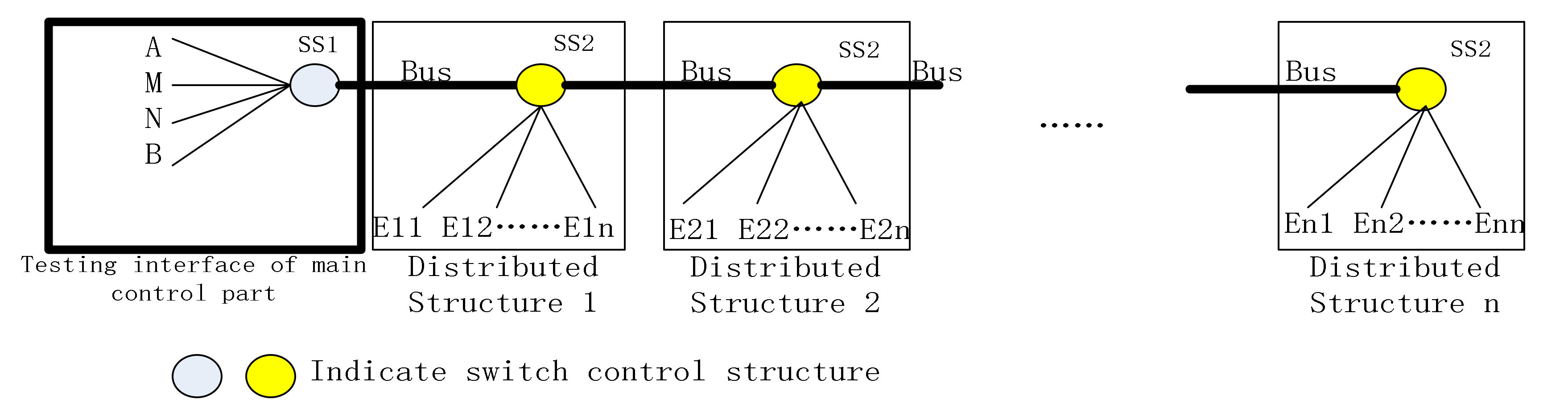
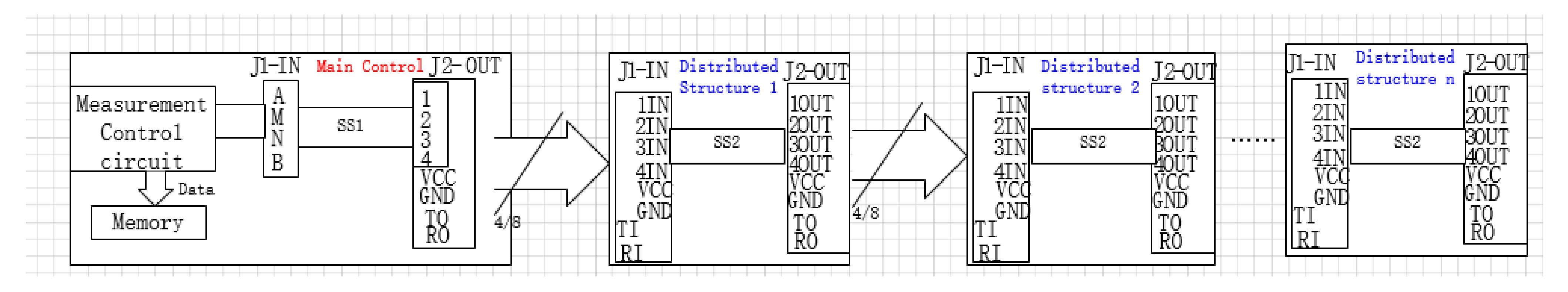
A distributed ERT instrument is usually comprised of one main control structure and multiple distributed structures with the same architecture. For discussion convenience, we used a Wenner test as an example, however other tests are similar. Details are shown in
Figure 1. The ports AMNB exist in the main control structure, and the electrodes exist in the distributed structures. The two parties interrelate with each other through the bus, consisting of four lines. To accomplish a single test, the four testing electrodes must be connected to AMNB in the correct order. The complete ERT survey is composed of back-to-back single resistivity tests. The task of ESD is to set up all test connections one by one in predetermined order. ESD is composed of many switch structures (SS). They exist in two parities, the main control and the distributed structure, as shown in
Figure 1. They are respectively called SS1 and SS2. Herein, SS1 is responsible for access of AMNB to the bus and SS2 is responsible for access of the four testing electrodes to the bus. Then, via the bus, two elements, AMNB and four testing electrodes, are interconnected.
2.2. Present ESDs
In 2004, Zheng Cai-jun designed an ESD for a distributed ERT, which is the most used model.
Figure 2 shows a SS1 schematic. It takes SPDT (Single Pole Double-Throw) and DPDT (Double Pole Double-Throw) switches to connect/disconnect the four ports of the AMNB to the bus lines.
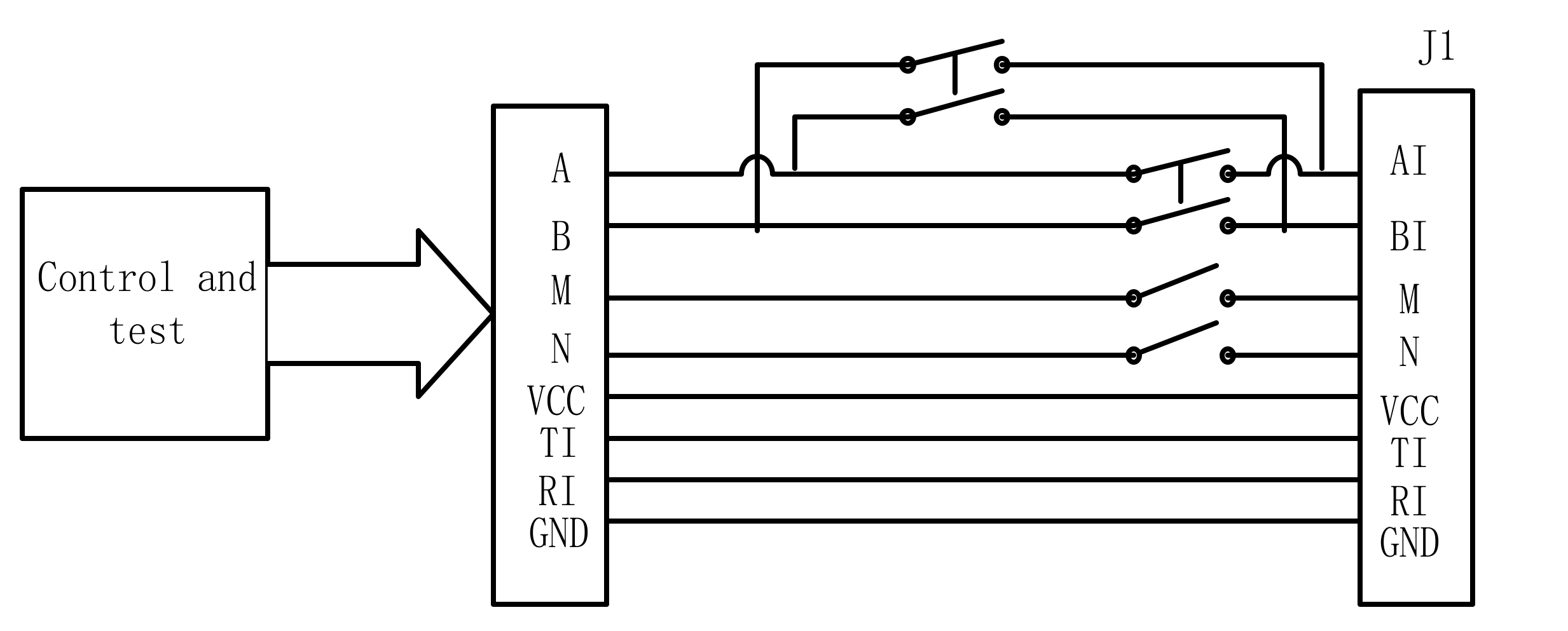
Figure 3 is the connection map of one of the electrodes in one distributed structure. It shows that four switches are required for each electrode. J1 in
Figure 2 is connected to J1 in
Figure 3 through bus lines (
Figure 1), and J2 is connected to J1 of the next electrode through the bus. Via this manner, all the electrodes are lapped to bus. Four switches are responsible for the connection between the electrode and one of the four connectors (AI, BI, MI, NI), and via the bus they set up a connection relationship with one of AMNB [
23].
As shown in
Figure 1, present traditional ESDs (TESD) have the same bus [
23,
24,
25]. The four lines on the bus are just one-to-one corresponding to AMNB four ports. In other words, SS1 just has the function of on and off, which is not a real structure. In SS2, an electrode must have four switches to choose one of the four lines (i.e., four ports). Analyzing all the information above, to improve the system structure SS1 must has its own function and not just act as a simple on-off to AMNB. It needs to set AMNB to not be directly connected to the fixed lines on the bus. Thus, it is possible that SS2 has other options, such as one electrode with less switches. This would divide the whole structure into two layers, which is completely different from the existing scheme. Accordingly, the newly designed ESD was named hierarchical ESD (HESD).
3. HESD Structure Design for ERT
HESD was realized through two-level topology. First, this section contrasts HESD to TESD, and further gives the hierarchical topology of HESD. Then, the detailed design of the two layers of the novel HESD is illustrated.
3.1. System Analyzing
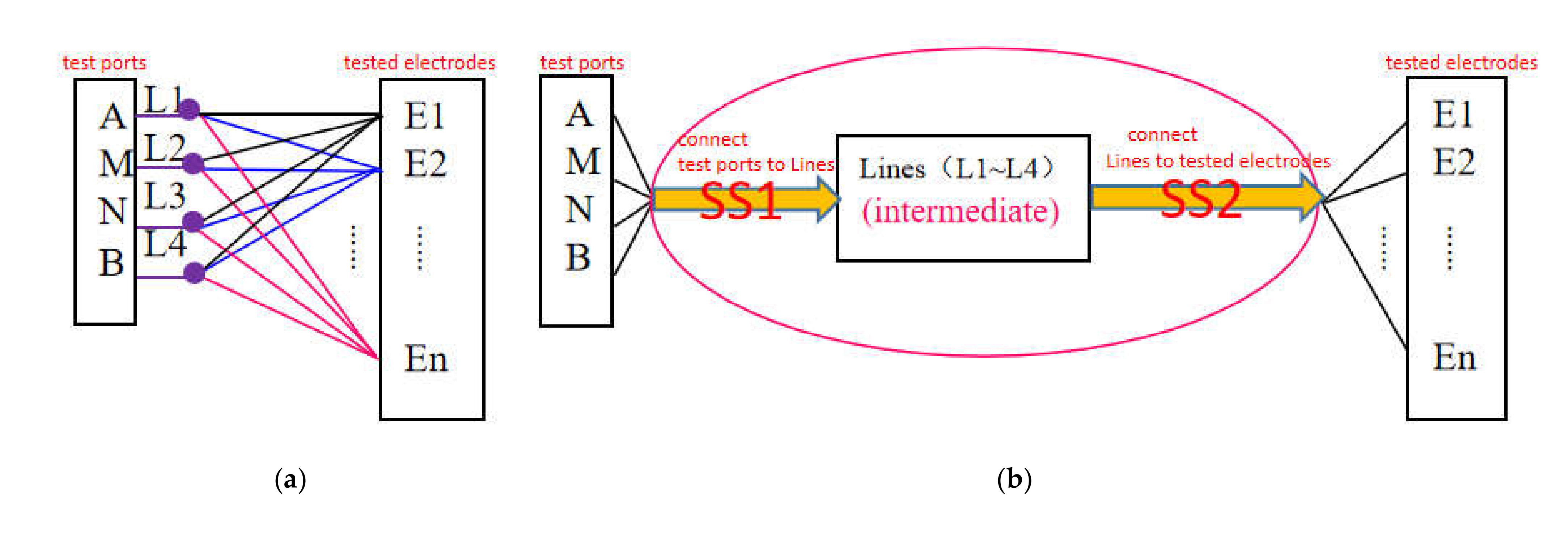
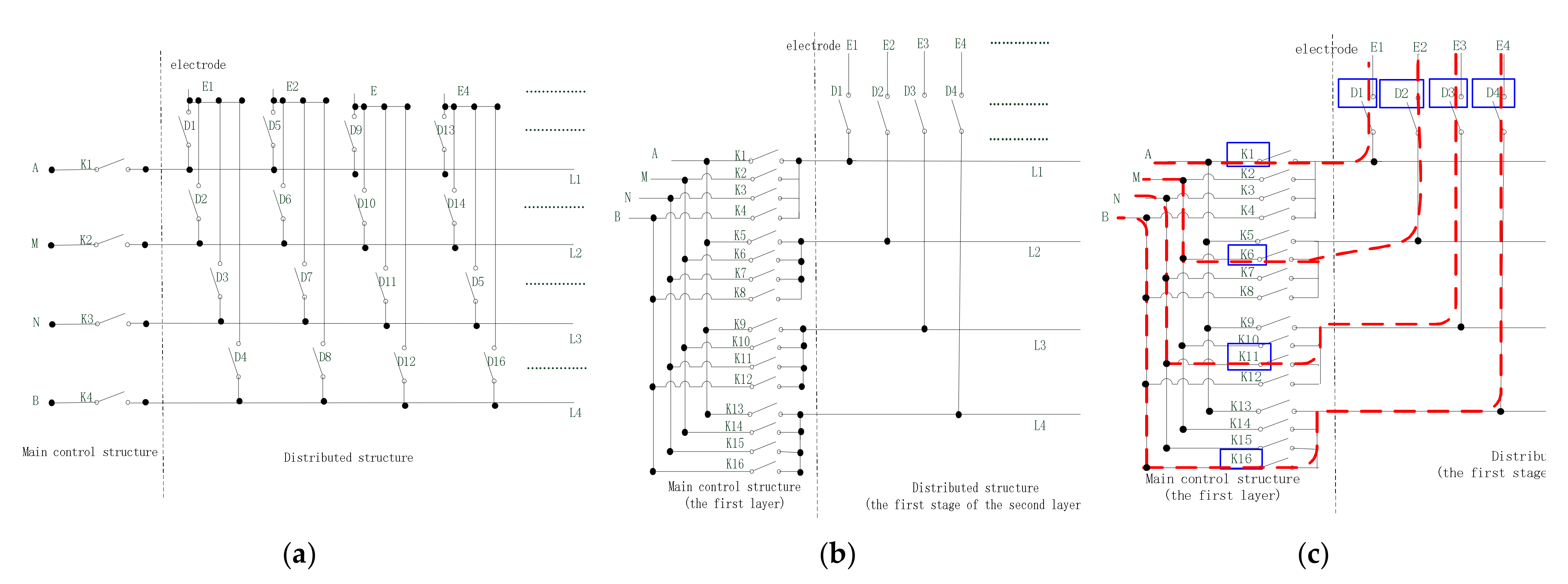
Figure 4a shows the topology structure of TESD. Four lines—L1, L2, L3, and L4 (L1–L4) —correspond to AMNB, and every electrode has four switches to control on/off. For instance, the four black lines from E1 need four switches to implement the make-and-break with AMNB. This means that one line has one switch.
As shown in
Figure 4b, the make-and-break operation between AMNB and each electrode is conducted through the bus (composed of L1–L4) as an intermediate instead of conducted directly. By employing this process, the whole ESD is divided into two layers, SS1 and SS2. The first layer SS1 performs on-off management between AMNB and L1–L4. To implement a test, an unrepeated link relationship must be set up between AMNB and L1–L4. For instance, A connects to L1 (A-L1), M–L3, N-L4, and B-L2. The second layer SS2 performs on-off management between L1–L4 and the four testing electrodes, i.e., L1-E1, L3-E2, L4-E3, and L2-E4. The two steps establish the connection between AMNB and the testing electrode E1–E4 as A-L1-E1, M-L3-E2, N-L4-E3, and B-L2-E4.
3.2. The First Layer SS1: Between AMNB and L1–L4
Figure 5 gives the topology structure of ESD in the main control, including TESD and the newly designed HESD. The TESD is constructed with one switch per port and one port directly corresponds with one line (
Figure 5a), while the first layer for HESD includes 16 switches (
Figure 5b). According to
Section 3.1, SS1 is transformed first. There is one switch per any of the ports for AMNB and the four lines (L1–L4), respectively. Herein, each port requires four switches, which will be treated as a single group. Four ports need 16 switches total (K1 to K16, called Series K). When testing, one of the four switches closes to connect the port to the line. With this setup, each line is able to connect to any port instead of connecting to a specific port. Therefore, the new HESD allows for choosing any line without restriction. In a different test, L1–L4 are mapped with different AMNB combinations. Each group of switches will set up one connection, e.g., A-K5-L2, M-K10-L3, N-K3-L1, and B-K16-L4, which would turn L1–L4 into NAMB.
3.3. The Second Layer SS2: Between L1–L4 and Electrodes
This layer is located at the distributed structures, which is further separated into two stages.
3.3.1. The First Stage (SS2-1): One-to-One Connection of Electrode and Line
Four I/O lines, L1–L4, come from main control parts and connect to distributed structures. They are, as a group, called the bus.
The distributed structure is responsible for controlling the connection status between lines and electrodes through Series D switches.
Figure 5 give the topology structure for the distributed parts of the TESD and the HESD. TESD needs four switches for one electrode (
Figure 5a), while HESD only needs one switch for one electrode (
Figure 5b). One distributed structure includes multiple electrodes, and four electrodes form a group. As shown in
Figure 5b, electrodes E1–E4 are connected successively to L1–L4 through switches D1–D4, and E5–E8 are connected successively to L1–L4 through switches D5–D8. The rest can be done in the same setting.
Implementing the first test in the ERT first layer (E1–E4 as testing electrodes connected to AMNB) requires set up connections, as shown in
Figure 5c. Close switch K1 to connect L1 and A, close K6 to connect L2 and M, close K11 to connect L3 and N, and close K4 to connect L4 and B. At the same time, close D1–D4 connects E1–E4 with L1–L4. In this way, through L1–L4, E1–E4 are linked together with AMNB ports. In this test, the whole concatenated relations are E1-D1-L1-K1-A, E2-D2-L2-K6-M, E3-D3-L3-K11-N, and E4-D4-L4-K16-B. The subsequent tests will be conducted in similar fashion. For example, the next test is the second test in the ERT first layer, and the connections are E2-D2-L2-K5-A, E3-D3-L3-K10-M, E4--D4-L4-K15-N, E5-D1-L1-K4-B, etc.
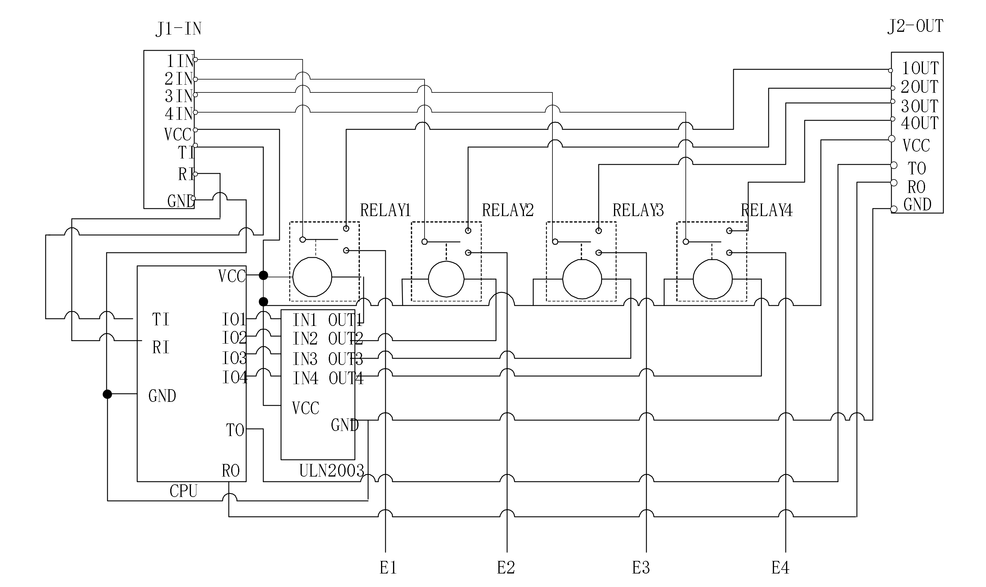
The circuit design scheme is acquired easily based on the structure in
Figure 5c. The circuit for HESD in each distributed structure or cell is shown in
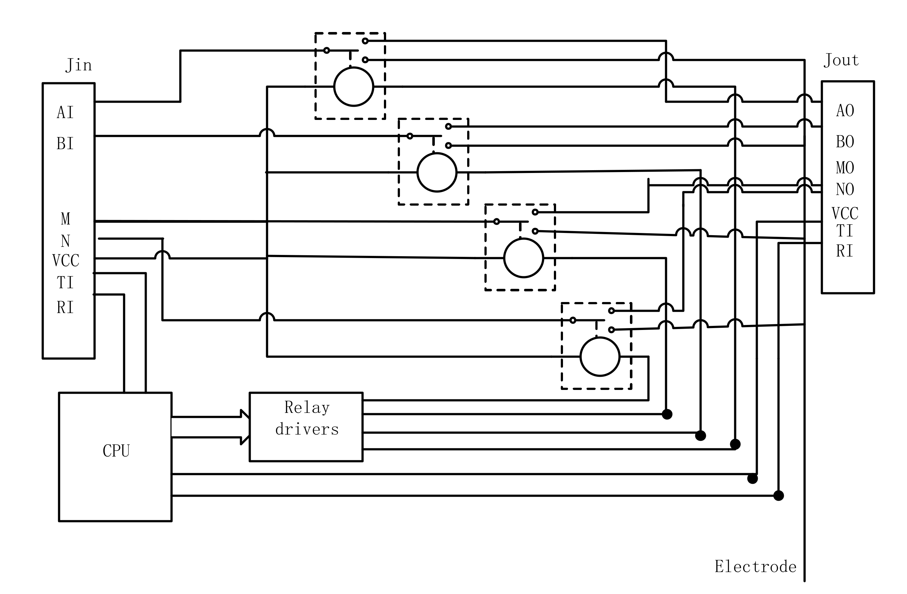
Figure 6 (four electrodes in a cell) as an example, and the structure for eight electrodes in a cell is likely. Conventionally, the most common plan is eight electrodes in one cell. Therefore, the distributed cell (structure) must contain an integer times four electrodes, which could be 4, 8, or 12 electrodes in a cell. In
Figure 6, the switch RELAY1 controls the 1IN to connect to 1OUT/E1. Connect to 1OUT means E1 need not connect to L1 and L1 will be left to subsequent cells, whereas connect to E1 means E1 connects to L1. In accordance with this process, the structure described above can finish the first layer test. However, whether it is able to complete any layer’s test needs to be studied.
HESD has the same SS1. Therefore, one switch is added for one additional electrode in SS2. This means that one electrode could likely only be connected to one predetermined line, e.g., E1 only to L1, E2 only to L2, etc. (
Figure 5c). This condition is denoted as a connection condition determined by the designed topology structure. It is noteworthy that the system tests claim that four testing electrodes must be one-to-one connected to four lines (L1–L4). Any two or more testing electrodes cannot be linked to the same line. This condition is denoted as the test condition. Obviously, the connection condition is acceptable or correct when it meets the test condition. To indicate if the two conditions are matched to each other, electrodes and their relevant lines are shown in
Table 1 for the foremost four tests in layer 1–layer 8 (the condition of other layers can be deduced from
Table 1). In
Table 1, in odd layers each electrode pairs with one line, e.g., the testing electrodes are connected to four different lines—L1, L4, L3, and L2 in the first test of the third layer. They fulfill the request. But in even layers, this is not the case. In the first and the third test of the second layer, four electrodes are paired with L1, L3, L1, and L3, respectively. Apparently, four testing electrodes in the even layers match to two lines (blue color) or one line (red color), but not four lines. These tests do not meet the test condition. It is demonstrated that the HESD with the first stage only works for tests of odd layers or the 1D test. Accordingly, we named it HESD-O. As described in
Section 1, the 1D test is very important and has wide applications. That means that a second stage of SS2 is required for HESD to be suitable for all conditions.
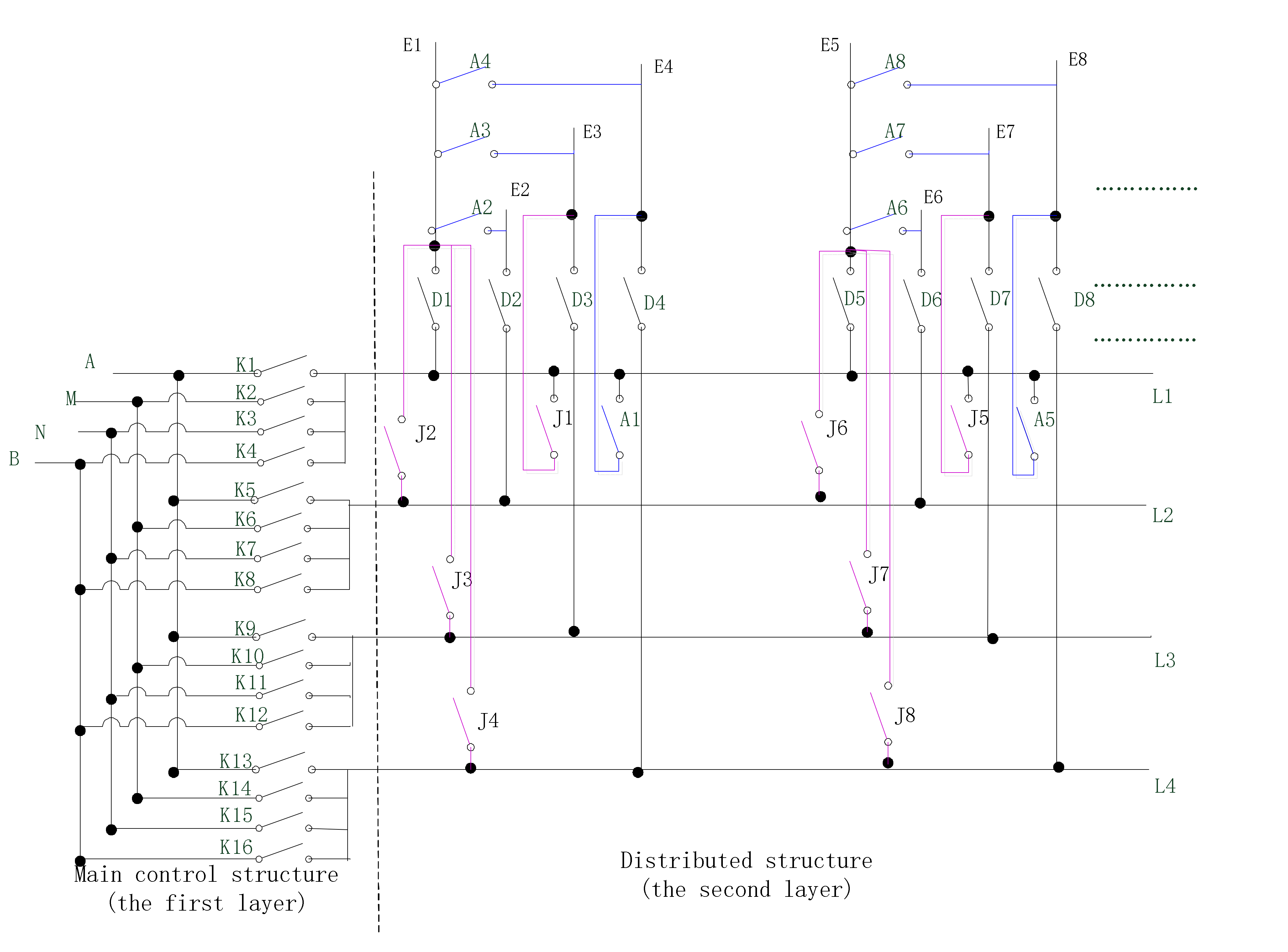
3.3.2. The Second Stage (SS-2): One-to-Four Connection of Electrodes and Lines
The improved HESD will work for any layer tests. To implement this task, the electrode can choose any line to connect with. The HESD is realized through adding switches in Series J and Series A (
Figure 7).
Series J is a series of switches designed to solve the problem of L1L3L1L3. In
Section 3.3.1, the problem in the first and the third test of layer two is the so-called L1L3 problem. Every four electrodes are added to four Series J switches. E1–E4 add J1–J4, in which J1 makes E3 connected to L1, and J2–J4 makes E1 connected to L2–L4. With these improvements, the L1L3 problem is solved by switching one pair of L1L3 to L2L4, so four testing electrodes will be connected to four lines of L1–L4, respectively. In this pattern, realization for the first test in the second layer is: E1-J2-L2, E3-J1-L1, E5-J8-L4, and E7-D7-L3. All L1L3 problems can be solved with the same mode.
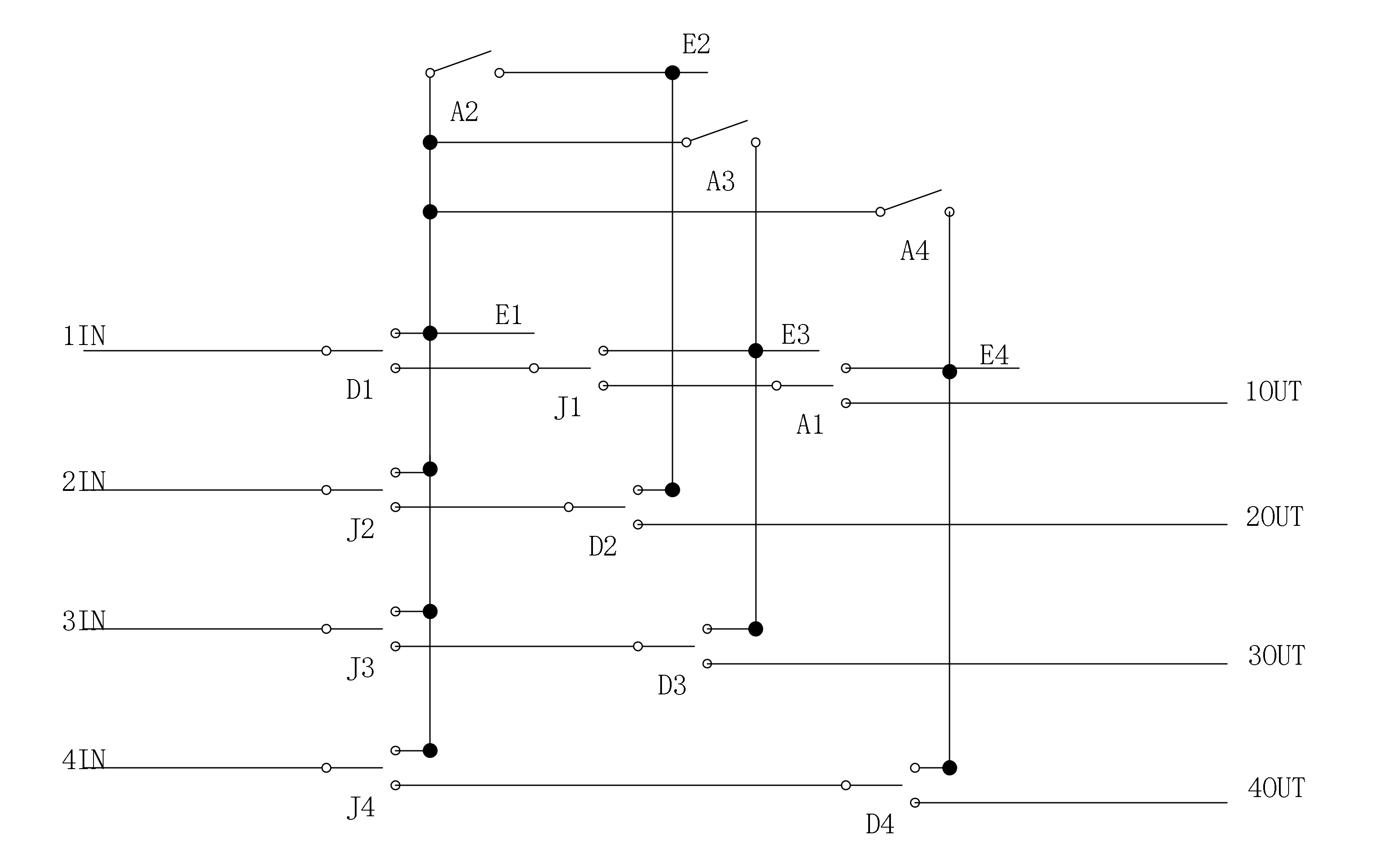
Based on series J, Series A is designed to further solve the L2L4 problem and one-line problem. The L2L4 problem appears at the second test in layer 2, where four testing electrodes correspond to L2L4L2L4, which means that two electrodes are linked to the same line. The one-line problem is that four testing electrodes all match with one line. The above two problems could be settled by adding four Series A switches for four electrodes. Taking E1–E4 cell as an example, switches A1–A4 are added as shown in
Figure 7. A1 links E4 to L1. A2–A4 link E2–E4 to E1, and D1 through to J2–J4 connect to any line of L1–L4. When the L2L4 problem happens, one pair of electrodes corresponding to L2L4 is adapted to L1L3 via Series A and Series J switches. A L2L4 problem for the second test in layer 4 is solved as: E2-A2-D1-L1, E6-D6-L2, E10-A10-J11-L3, and E14-A14-J16-L4. When a one-line problem appears, a similar mode is fixed. The specific schematic for distributed cells is described in
Figure 8, which takes four electrodes as a cell or group.
In the second stage of SS2 in the distributed ERT system, Series J and Series A switches are added to solve problems that emerged in even layers. This helps the whole system adapt to any conditions (HESD-A), including the odd layers or 1D test.
With SS2 having been added to HESD-O, the entire HESD is finished and can be applied to any condition. The ERT profile is shown in
Appendix A (
Figure A1).
4. Results
The number of electrodes can be calculated as 16 + e*1 for HESD-O applications and as 16 + e*3 for HESD-A, whereas TESD is computed as 4 + e*4. In these formulas, e indicates the number of electrodes.
Table 2 lists the results to compare different requests in different ESD designs. When e > 4, HESD-O needs less switches than TESD, and when e > 16, HESD-A needs less switches than TESD. In most ERT systems, several hundreds of electrodes are employed [
26,
27].
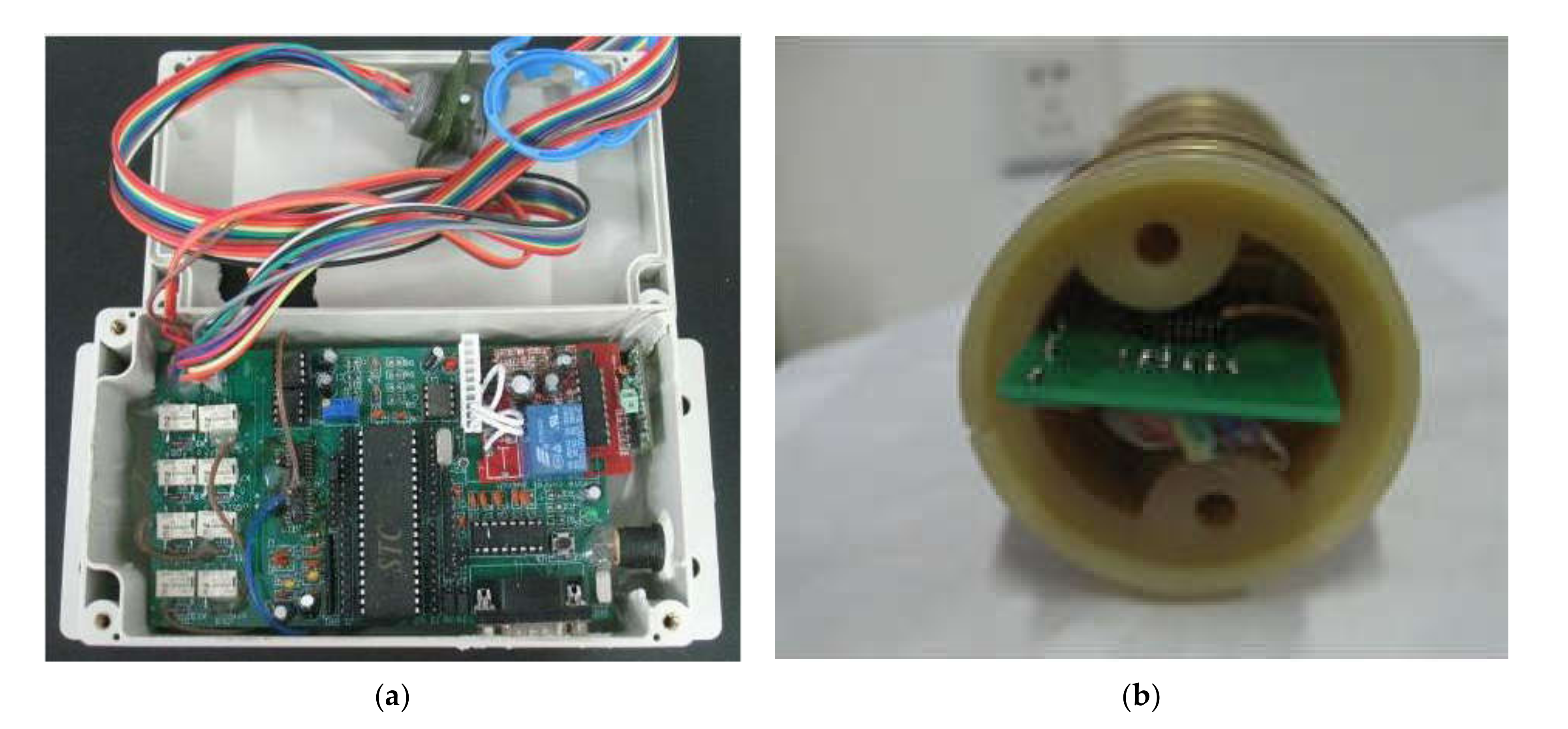
The results in this article were employed in a real ERT system. The HESD-O structure was used to construct a ERT testing system (with 100 electrodes) to realize seabed sediment and suspended sediment testing [
16,
28]. The main control circuit is shown in
Figure 9a and the distributed circuit encased in the testing probe is shown in
Figure 9b.
5. Discussion
The newly designed HESD for distributed ERT instrument saves hardware expenditure through the elaborate structure design in hardware, although the software that controls HESD needs to be changed accordingly, which is rather simple. If the total number of electrodes is less than eight, using the HESD is not recommended since will change both the software and hardware design. In the future, using other kinds of switches with new ideas, further research about more economic structures may be possible.
6. Conclusions
The article aimed to solve the hardware expenditure problem. Based on analyzing the pre-existing switching devices, a novelty electrode switching device HESD was developed for a distributed ERT instrument. It employs a new design style completely different from the conventional one. It uses a hierarchical structure in which the connections between electrodes and AMNB ports are not conducted directly, but instead it employs the four lines of L1–L4 as intermediates. The integrated HESD is composed of Series K, Series D, Series J and Series A switches, which belong to two layers: SS1 and SS2. In this article, the whole design is divided into three parts: SS1, SS2-1 and SS2-2.
First is the SS1 structure or first layer design. Series K belongs to SS1. With 16 switches, they can connect AMNB to any combination of L1–L4. Other series all belong to SS2, which achieve the links between L1–L4 and four testing electrodes. The SS2 is divided into two stages.
Then there is the SS2-1 design. SS2-1 contains four switches of Series D for a four-electrode cell, which takes one electrode to one line. Applying SS1 and the first stage of SS2, HESD-O easily facilitated the electrode connection for the 1D profile test or odd layer’s test. This could save up to three fourths the number of switches and related expenditure, including related hardware, power, and volume. It is especially beneficial in-situ tests and portable instruments.
The third part is SS2-2. SS2-2 fixes the L1L3 problem, L2L4 problem, and one-line problem, and possesses a complex frame. Furthermore, applying the entire plan of HESD-A, all layers’ 2D ERT tests can be settled, which also saves one fourth the number of switches. A saved hardware plan for the ESD design is provided in the article. The two designs of HESD, HESD-O and HESD-A, are suitable for different demands, respectively. Although they may bring new software designs, they significantly save on hardware expenditure and are more miniature, especially for multi-electrodes, e.g., several dozen or more single-channel ERT systems.
7. Patents
There are patents resulting from the work reported in this manuscript.
Xin Xia. An electrode switching device (ESD) suitable for a kind of layered electrical resistivity tomography (ERT): China, CN201510585837.1 [P], 2016-05-18.
Xin Xia. Electrode switching device (ESD) for distributed cycling electrical resistivity tomography (ERT): China, CN201120276534.9[P]. 2012-4-4.
Author Contributions
Conceptualization, X.X.; methodology, X.X.; software, X.X.; validation, Y.-Y.P. and X.-L.L.; formal analysis, X.X.; investigation, X.X.; resources, Y.-G.J.; data curation, Y.-Y.P.; writing—original draft preparation, X.X.; writing—review and editing, Y.-Y.P. and X.-L.L.; visualization, X.X.; supervision, Y.-G.J.; project administration, X.X.; funding acquisition, Y.-G.J. All authors have read and agreed to the published version of the manuscript.
Funding
This research was funded by the National High Technology Research and Development Program of China, grant number 2008AA09Z109; the National Natural Science Foundation of China, grant number 40876042; and the Young Scientists Fund of the National Natural Science Foundation of China, grant number 41502261.
Institutional Review Board Statement
Not applicable.
Informed Consent Statement
Not applicable.
Data Availability Statement
Not applicable.
Acknowledgments
We are grateful to all the members of the GEE Group of Ocean University of China. The cooperation of the group assisted in the accomplishment of this manuscript.
Conflicts of Interest
The authors declare no conflict of interest.
References
- Daily, W.; Owen, E. Cross-Borehole Resistivity Tomography. Geophysics 1991, 56, 1228. [Google Scholar] [CrossRef]
- Shima, H. Resistivity Tomography: An Approach to 2-Dresistivity Inverse Problems. In Proceedings of the Annual Meeting of Society of Exploration Geophysicists, New Orleans, LO, USA, 11–15 October 1987; pp. 59–61. [Google Scholar]
- Bellmunt, F.; Marcuello, A.; Ledo, J.; Queralt, P. Capability of Cross-Hole Electrical Configurations for Monitoring Rapid Plume Migration Experiments. J. Appl. Geophys. 2016, 124, 73–82. [Google Scholar] [CrossRef]
- Kowalczyk, S.; Zwrzykraj, P.; Mieszkowski, R. Application of Electrical Resistivity Tomography in Assessing Complex Soil Conditions. Geol. Q. 2015, 59, 367–372. [Google Scholar] [CrossRef]
- Cao, L.; Meng, Y.; Zhou, J. Review and Prospect of Resistivity Tomography Technology. Prog. Explor. Geophys. 2004, 3. [Google Scholar]
- Zainal, M.; Munir, B. The Electrical Resistivity Tomography Technique for Landslide Characterization in Blangkejeren Aceh. J. Phys. Conf. Ser. 2021, 1825, 012022. [Google Scholar] [CrossRef]
- Dong, H.B.; Wang, C.-L. Development and Application of 2d Resistivity Imaging Survey. Earth Sci. Front. 2003, 1, 171–176. [Google Scholar]
- Wu, C.; Liu, S.-D.; Qiu, Z.-L. Technology of Network Parallel Electric Method Applied to Detection of Water Ponding in Mining Goaf. Coal Sci. Technol. 2013, 4, 93–95. [Google Scholar]
- Zheng, X.-L.; Liu, S.-D. Design on Parallel Collection Network Electrical Instrument Based on Double Processors. Coal Sci. Technol. 2008, 4, 85–88. [Google Scholar]
- Liu, S.-D.; Wu, R.-X.; Zhang, P.-D. Three-Dimensional Parallel Electric Surveying and Its Applications in Water Disaster Exploration in Coal Mines. J. China Coal Soc. 2009, 7, 927–932. [Google Scholar]
- Wu, C.-F.; Qiu, Z.-L.; Yang, S.-L. A Comparison of Advanced Detection Effect between the Network Parallel Electrical Method and the Traditional Method. Geophys. Geochem. Explor. 2015, 1, 136–140. [Google Scholar]
- Kim, K.-J.; Cho, I.-K. Time-Lapse Inversion of 2d Resistivity Monitoring Data with a Spatially Varying Cross-Model Constraint. J. Appl. Geophys. 2011, 74, 114–122. [Google Scholar] [CrossRef]
- Hu, S.-G.; Liu, S.-D. A Comparative Study of Efficiency About Traditional Electrical and Collateral Electrical Data Collection in Electrical Prospecting. Prog. Geophys. 2010, 25. [Google Scholar]
- Samouёliana, A.; Cousin, I.; Tabbagh, A.; Bruand, A.; Richard, G. Electrical Resistivity Survey in Soil Science: A Review. Soil Tillage Res. 2005, 83, 173–193. [Google Scholar] [CrossRef] [Green Version]
- Ridd, P.V. A Sediment Level Sensor for Erosion and Siltation Detection. Estuar. Coast. Shelf Sci. 1992, 35, 353–362. [Google Scholar] [CrossRef]
- Xia, X. In-Situ Monitoring Technology Study of Seabed Erosion and Depositon Proeess Based on Resistivity Method. Ocean Univ. China 2009, 1, 48–49. [Google Scholar]
- Fukue, M.; Minato, T.; Matsumoto, M.; Horibe, H.; Taya, N. Use of a Resistivity Cone for Detecting Contaminated Soil Layers. Eng. Geol. 2001, 60, 361–369. [Google Scholar] [CrossRef]
- Faries, J.W. A New Conductivity Sediment Concentration Profiler (Ccp) for the Measurement of Nearbed Sediment Concentrations: Application in the Swash Zone on a Laboratory Beach; University of Delaware: Newark, DE, USA, 2009. [Google Scholar]
- Puleo, J.A.; Faries, J.; Davidson, M.; Hicks, B. A Conductivity Sensor for Nearbed Sediment Concentration Profiling. J. Atmos. Ocean. Technol. 2010, 27, 397–408. [Google Scholar] [CrossRef]
- Nasr-El-Din, H.; Shook, C.A.; Colwell, J. A Conductivity Probe for Measuring Local Concentrations in Slurry Systems. Int. J. Multiph. Flow 1987, 13, 365–378. [Google Scholar] [CrossRef]
- Arnaud, G.; Mory, M.; Abadie, S.; Cassen, M. Use of a Resistive Rods Network to Monitor Bathymetric Evolution in the Surf/Swash Zone. J. Coast. Res. 2009, 56, 1781–1785. [Google Scholar]
- Wheatcroft, R.A. In Situ Measurements of near-Surface Porosity in Shallow-Water Marine Sands. IEEE J. Ocean. Eng. 2002, 27, 561–570. [Google Scholar] [CrossRef]
- Zheng, C.-J. The Design for Electrode Change Device of Distributed High Density Resistivity Instrument. Equip. Geotech. Eng. 2004, 5, 34–37. [Google Scholar]
- Yang, H.-Z. The Manufacture of Electrical Prospecting Subsidiary Devices. Geophys. Gepchem. Explor. 2010, 34, 623–634. [Google Scholar]
- Li, Y. New High-Density Electrical Apparatus Study for Mining Background. Master’s Thesis, Northwest University, Kirkland, WA, USA, 2014. [Google Scholar]
- Ogilvy, R.D.; Meldrum, P.I.; Kuras, O.; Wilkinson, P.B.; Chambers, J.E.; Sen, M.; Pulido-Bosch, A.; Gisbert, J.; Jorreto, S.; Frances, I. Automated Monitoring of Coastal Aquifers with Electrical Resistivity Tomography. Near Surf. Geophys. 2009, 7, 367–375. [Google Scholar] [CrossRef] [Green Version]
- Chambers, J.E.; Kuras, O.; Meldrum, P.I.; Ogilvy, R.D.; Hollands, J. Electrical Resistivity Tomography Applied to Geologic, Hydrogeologic, and Engineering Investigations at a Former Waste-Disposal Site. Geophysics 2006, 71, 231–239. [Google Scholar] [CrossRef] [Green Version]
- Jia, Y.; Li, H.; Meng, X.; Liu, X. Deposition-Monitoring Technology in an Estuarial Environment Using an Electrical-Resistivity Method. J. Coast. Res. 2012, 28, 860–867. [Google Scholar]
| Publisher’s Note: MDPI stays neutral with regard to jurisdictional claims in published maps and institutional affiliations. |
© 2021 by the authors. Licensee MDPI, Basel, Switzerland. This article is an open access article distributed under the terms and conditions of the Creative Commons Attribution (CC BY) license (https://creativecommons.org/licenses/by/4.0/).


