
Substrate-Driven Atomic Layer Deposition of High-κ Dielectrics on 2D Materials


Consiglio Nazionale delle Ricerche, Istituto per la Microelettronica e Microsistemi, Strada VIII, 5, 95121 Catania, Italy
*
Authors to whom correspondence should be addressed.
Appl. Sci. 2021, 11(22), 11052; https://0-doi-org.brum.beds.ac.uk/10.3390/app112211052
Submission received: 3 November 2021
/
Revised: 16 November 2021
/
Accepted: 18 November 2021
/
Published: 22 November 2021
(This article belongs to the Special Issue Applications of Graphene Family Materials for Environmental Sensing)
Abstract
:Atomic layer deposition (ALD) of high-κ dielectrics on two-dimensional (2D) materials (including graphene and transition metal dichalcogenides) still represents a challenge due to the lack of out-of-plane bonds on the pristine surfaces of 2D materials, thus making the nucleation process highly disadvantaged. The typical methods to promote the nucleation (i.e., the predeposition of seed layers or the surface activation via chemical treatments) certainly improve the ALD growth but can affect, to some extent, the electronic properties of 2D materials and the interface with high-κ dielectrics. Hence, direct ALD on 2D materials without seed and functionalization layers remains highly desirable. In this context, a crucial role can be played by the interaction with the substrate supporting the 2D membrane. In particular, metallic substrates such as copper or gold have been found to enhance the ALD nucleation of Al2O3 and HfO2 both on monolayer (1 L) graphene and MoS2. Similarly, uniform ALD growth of Al2O3 on the surface of 1 L epitaxial graphene (EG) on SiC (0001) has been ascribed to the peculiar EG/SiC interface properties. This review provides a detailed discussion of the substrate-driven ALD growth of high-κ dielectrics on 2D materials, mainly on graphene and MoS2. The nucleation mechanism and the influence of the ALD parameters (namely the ALD temperature and cycle number) on the coverage as well as the structural and electrical properties of the deposited high-κ thin films are described. Finally, the open challenges for applications are discussed.
1. Introduction
Two-dimensional (2D) materials such as semi-metallic graphene and the semiconducting transition metal dicalchogenides (TMDs) have been the object of intensive research investigations in the last 15 years due to their wide range of potential applications in electronics, optoelectronics, and sensing. As an example, the excellent carrier mobility (103–105 cm2/Vs) [1] and micrometer electron mean free path [2] of graphene have been exploited in the demonstration of high-frequency (100–300 GHz) transistors [3,4], for which the low on/off current ratio (due to the lack of an energy bandgap) represents a minor issue. On the other hand, semiconducting TMDs (including MoS2, WS2, MoSe2, and WSe2) are currently regarded as the most suitable channel materials for ultra-thin body field effect transistors to be employed in next-generation logic or switching applications [5,6]. As an example, transistors with high on/off current ratios (106–108) and low subthreshold swings (SS ≈ 70 meV/decade) [7,8] have been fabricated using monolayer (1 L) MoS2 (with a direct bandgap of 1.8 eV) or multilayer MoS2 (with an indirect bandgap of 1.2 eV) [9,10].
Practical implementation of electronic devices based on 2D materials requires their combination with high-κ dielectrics, such as Al2O3, HfO2, and ZrO2. In the case of top-gated field effect transistors with graphene or MoS2 channels, high-κ gate insulators are necessary for efficient electrostatic control of the lateral source-to-drain current while minimizing the gate leakage phenomena [11,12,13]. Furthermore, the encapsulation of the monolayer or multilayers of MoS2 with high-κ dielectrics has been demonstrated to be highly beneficial in the improvement of the field effect mobility up to 200–500 cm2 V−1s−1 due to the efficient reduction of charged impurity scattering [7,8,14]. Obviously, with the scaling down process which invests the electronic field, most of these applications require high-κ dielectrics in the form of uniform and ultra-thin layers. Aside from conventional field effect transistor structures, novel device concepts and architectures also require the integration of high-quality and ultra-thin insulators on the surfaces of 2D materials [15,16]. As an example, the recently investigated graphene-base hot electron transistors (GBHETs) for THz electronics require the integration of an ultra-thin insulator on graphene working as a base collector tunnel barrier for vertical transport [17,18,19]. Furthermore, graphene sensors may involve high-κ deposition on graphene as a functional layer toward specific chemical and biological molecules [20].
In this context, the atomic layer deposition (ALD) is the most appropriate technique for the growth of ultra-thin layers, with accurate control of the thickness and surface coverage. However, the surface of pristine 2D materials is chemically inert toward the chemical reactions involved in the ALD process, typically resulting in inhomogeneous coverage by the deposited films. To overcome this inherent issue, several approaches have been investigated in order to promote ALD growth on 2D crystals, including the predeposition of seed layers and surface activation via chemical treatments. As a matter of fact, these methods present advantages and disadvantages, ultimately affecting the final performance of graphene or MoS2 devices. Hence, the direct (i.e., pre-functionalization and seed layer-free) ALD growth of high-κ dielectrics on the pristine surface of 2D materials still remains highly desirable and has been the object of investigation in recent years. As an alternative to surface pretreatments of 2D materials, some research groups recently considered the possibility of exploiting their peculiar interaction with the underlying substrate as a way to enhance the ALD nucleation process. As an example, Dlubak et al. [21] demonstrated the direct ALD growth of uniform Al2O3 layers on 1 L graphene as grown by CVD on metal substrates (Cu and Ni-Au). More recently, Schilirò et al. [22] showed the deposition of highly homogeneous and ultra-thin Al2O3 films by direct thermal ALD on 1 L MoS2 supported by a gold (Au) substrate. In both cases, the high-quality ALD growth was explained by the enhanced adsorption of the ALD precursor molecules on 1 L graphene or MoS2 surfaces during the nucleation stage. This was ascribed, in part, to the action of electrostatic fields induced by charges at the interface with the metal substrate [23,24], as well as the partial transparency of the atomically thin 2D materials to the electric fields [25]. Such a beneficial role of 2D material and substrate interaction on the high-κ nucleation in ALD processes is not limited to the case of metal substrates. In fact, the direct ALD growth of uniform Al2O3 films has also been recently reported for 1 L epitaxial graphene on SiC (0001), and it has been ascribed to the electrostatic effect of positively charged dangling bonds related to the buffer layer at the graphene/SiC interface [26,27].
While the state of the art of ALD on 2D materials has been the object of different comprehensive review papers in recent years [28,29,30], a dedicated review article on the direct ALD growth of high dielectrics driven by the 2D material and substrate interaction is still missing. The aim of the present work is to provide an overview in this research topic. After a discussion on the advantages and disadvantages of the conventional approaches (seed layer and pre-functionalization treatments) used to promote ALD growth on graphene and TMDs, this paper will focus on the direct thermal ALD of high-κ dielectrics (mainly Al2O3 and HfO2) on CVD graphene on Cu (or Ni), on epitaxial graphene on 4H-SiC (0001), and on exfoliated MoS2 on gold. The role of the interaction with the underlying substrate and the relevant process parameters (i.e., the ALD temperature and number of cycles) on the coverage will be discussed. Furthermore, the morphological and electrical properties of the grown high-κ layers will be illustrated. Finally, the current status and open challenges for applications of the high-κ/2 M material systems will be critically examined.
2. Atomic Layer Deposition on 2D Materials
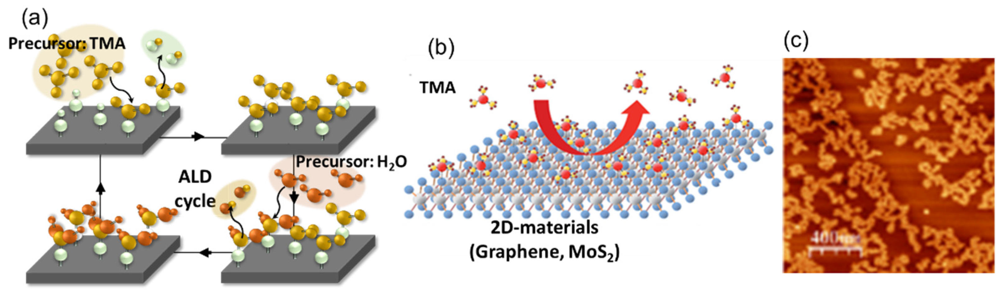
The ALD is the most suitable deposition technique for the growth of ultra-thin and conformal dielectric layers on a substrate. The key strength of ALD is related to its peculiar deposition mechanism. It is based on sequential and self-limited chemical reactions between the properly selected chemical precursors and the active sites of the substrate surface, which results in the so-called layer-by-layer growth mode (see Figure 1a). This characteristic principle of growth allows for obtaining uniform, conformal, and pinhole-free depositions with angstrom-level control of the thickness in a large area [31]. However, ALD implementation on a pristine surface of graphene and other 2D materials is a difficult task due to the lack of dangling bonds working as active sites or functional groups for the adsorption of ALD precursors (as depicted in Figure 1b). The main consequence of this feature is a lack of deposition or the formation of inhomogeneous films (e.g., see the image of ALD-Al2O3 on the pristine MoS2 surface in Figure 1c).
2.1. Methods to Promote ALD Growth on 2D Materials
To date, a wide variety of processes has been reported to promote ALD nucleation on 2D layered materials, which finally results in the deposition of uniform dielectric layers. Table 1 reports a selection of the literature results for different types of 2D materials, with the indication of the used surface activation for ALD, the deposited high-κ insulator, its thickness and uniformity, and eventual damage introduced in the 2D material by the ALD process.
From the historical point of view, most of these approaches have been developed for graphene [35,37,55,56], and many of them have been adapted to other layered materials, such as TMDs [36]. These processes can be grouped into two categories:
- (i)
- Predeposition of a seed-layer;
- (ii)
- Chemical pre-functionalization.
The seed layers can be of both an organic nature, such as self-assembled monolayers (SAM) [34,57] or spin-coated polymers layers [35,36,55], and an inorganic nature, such as sputtered or evaporated metal or metal oxide films [37,38,39,56] or SiO2 nanoparticles [40]. They can be pre-deposited “ex situ” (i.e., outside the ALD reactor chamber) and also “in situ” (i.e., within the reactor), like in the case of low temperature H2O-assisted dielectric seed layer growth on the surface of graphene [41,42].
The seed layer approach proved to be an efficient and widely used method to promote the subsequent ALD growth process on graphene and TMDs. Typically, the spin-coating, self-assembling, and physical deposition methods (e.g., evaporation) used to deposit seed layers result in limited damage to the 2D membranes. However, from the electrical point of view, poor interface quality between the seed layer and 2D materials can result in a high-density interface or near-interface traps, ultimately compromising the performances of the final device. On the other hand, the metal seed layer deposition has been found to be beneficial for protecting the structural and electrical properties of the 2D material from the following ALD process. In particular, recent reports on the ALD deposition of ZrO2 on MoS2 [38,39] demonstrated that the Al seed layer reduces the oxidation effect of the 2D material by the co-reactant (H2O, O3) during the ALD process, mainly for the O3-based method. Moreover, the introduction of a seed layer limits the minimum achievable thickness of the high-κ film, and this can represent a serious concern for the downscaling of 2D material-based transistors.
Chemical pretreatments of a 2D material surface, such as exposure to NO2 [45], O3 [33,46,47,48] or O2-plasma [50,51], and N2-plasma [52], introduce functional groups or dangling bonds, enabling the ALD nucleation and growth of high-κ dielectrics. These approaches allow, in principle, the growth of ultra-thin insulating films, but at the same time, they can introduce defects in the 2D layer, degrading its electronic properties.
Aside from the seeding layer and chemical pretreatments, the ALD process conditions (e.g., the deposition temperature and the pulse and purge times) can play a key role in achieving uniform coverage of a 2D material’s surface. ALD depositions of Al2O3 or HfO2 are typically carried out in a temperature window from 200 to 300 °C, which ensures the optimal reaction of the precursors. However, lower deposition temperatures allow higher physisorption of the precursors on the graphene or TMD surface, improving ALD nucleation [32,41,53]. As an example, Aria et al. [53] demonstrated improved coverage and uniformity of deposited films on graphene within a temperature window of 80–100 °C for both Al2O3 and HfO2 materials. In particular, optimized ALD coverage (up to 98%) was demonstrated using prolonged pulse times (>2 s) [53].
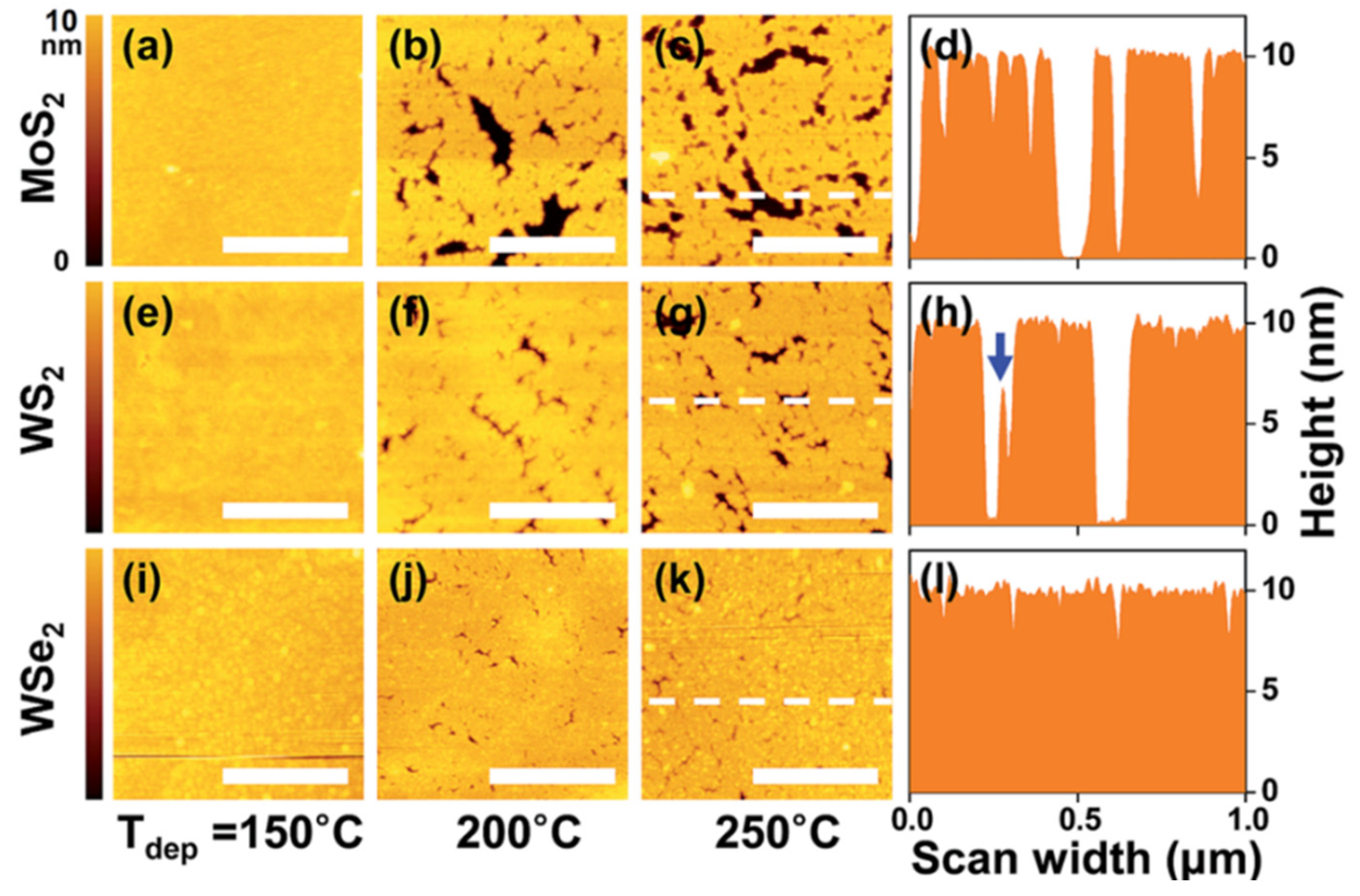
Recently, Park et al. [32] reported a systematic study on the thermal ALD of Al2O3 on the surface of multilayers of TMDs (MoS2, WS2, and WSe2) using different deposition temperatures (see Figure 2). Inhomogeneous Al2O3 layers (with a large density of pinholes) were obtained using the conventional temperatures of 200–250 °C, whereas uniform coverage was observed when lowering Tdep to 150 °C. Furthermore, at the same deposition temperature, better uniformity of the deposited Al2O3 (~10 nm) films was observed on WSe2 and on WS2 than on MoS2. This was ascribed to the larger polarizability of the W-and Se-based TMDs, giving rise to a higher adsorption energy of the TMA precursor due to electrostatic interaction.
A two-step ALD process with early low-temperature (80 °C) deposition of an ultra-thin AlOx layer and a following deposition at a higher temperature (180 °C) was also recently employed to obtain a homogeneous Al2O3 film with a <10 nm total thickness on MoS2 [43]. The low temperature, however, can be responsible for the degradation of the dielectric quality due to the reduced reactivity of the ALD precursor. In these conditions, the insulating films are generally characterized by a lower density and, consequently, by a lower dielectric constant [58].
2.2. Electrical Behavior and Interface Quality of High-κ Dielectrics by ALD on 2D Materials
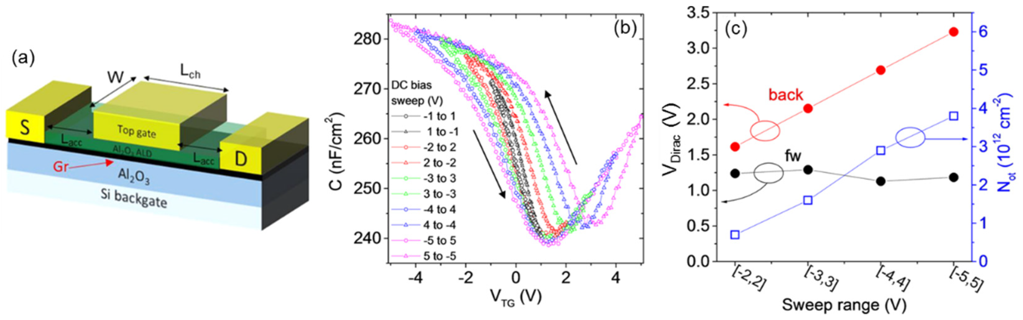
The quality of grown high-κ dielectrics and of their interface with the 2D material strongly influences the electrical performances of the final devices. The seed layer deposition, typically carried out ex situ, can introduce impurities and particles, which act as charge traps compromising the reliability of the high-κ dielectrics subsequently grown by ALD. Fallahazad et al. explained that the HfO2 deposited on graphene by the evaporated Al seed layer presents a relatively low permittivity (ε = 5.5) and a low-quality interface, which is characterized by impurities and defects responsible for mobility degradation [37,59]. Alternatively, a method based on the in situ deposition of a metal oxide H2O-assisted seed layer has been proposed [41,42]. This approach involves the physical adsorption (by Van Der Walls interactions) of a continuous layer of H2O molecules, which acts as a site of nucleation for a seed layer of high-κ dielectrics at a low temperature (100 °C), followed by conventional deposition at 200–250°C. Fisichella et al. [42] demonstrated that this approach ensures the optimal electrical features of the deposited dielectric on graphene, with a favorable permittivity (ε = 7.45) and breakdown field (EBD = 7.4 MV/cm). On the other hand, significant charge trapping at the Al2O3/graphene interface has been observed during the operation of top-gated field effect transistors (Figure 3a). In particular, the density of negative trapped charges up to ~4 × 1012 cm−2 was evaluated by capacitance voltage (C-VTG) measurements when increasing the forward and backward gate bias sweeps (Figure 3b,c).
Additionally, high-κ layers grown on 2D materials pre-functionalized by reactive gas species are subjected to charge trapping phenomena both at the interface and inside the dielectrics. As an example, the HfO2 top gate dielectric grown on a MoS2 surface after UV-O3 treatment [60] shows significant charge trapping, which can be ascribed to impurities and defects generated during the reactive gas exposure. Additionally, O2-plasma pretreatments have been shown to have an effect on the interfacial properties and, consequently, the performance of the dielectric [51,52]. As an example, Zhou et al. [61] demonstrated that remote O2-plasma is effective for the ALD growth of Al2O3 on graphene, but on the other hand, they found the formation of a defective interfacial layer, resulting in a low breakdown field for the oxide (1.2 MV/cm). As previously discussed, the temperature used during the ALD process plays an important role in the uniformity of the dielectric coverage. In particular, as demonstrated in [32,53,54], growth temperatures lower than 150 °C allow for achieving better uniformity, but at the same time, they result in a significant increase of trapping phenomena and, consequently, a degradation of the passivation degree [60,62].
3. Substrate-Driven ALD of High-κ Dielectrics on 2D Materials
3.1. ALD on Monolayer CVD Graphene on the Native Metal Substrates
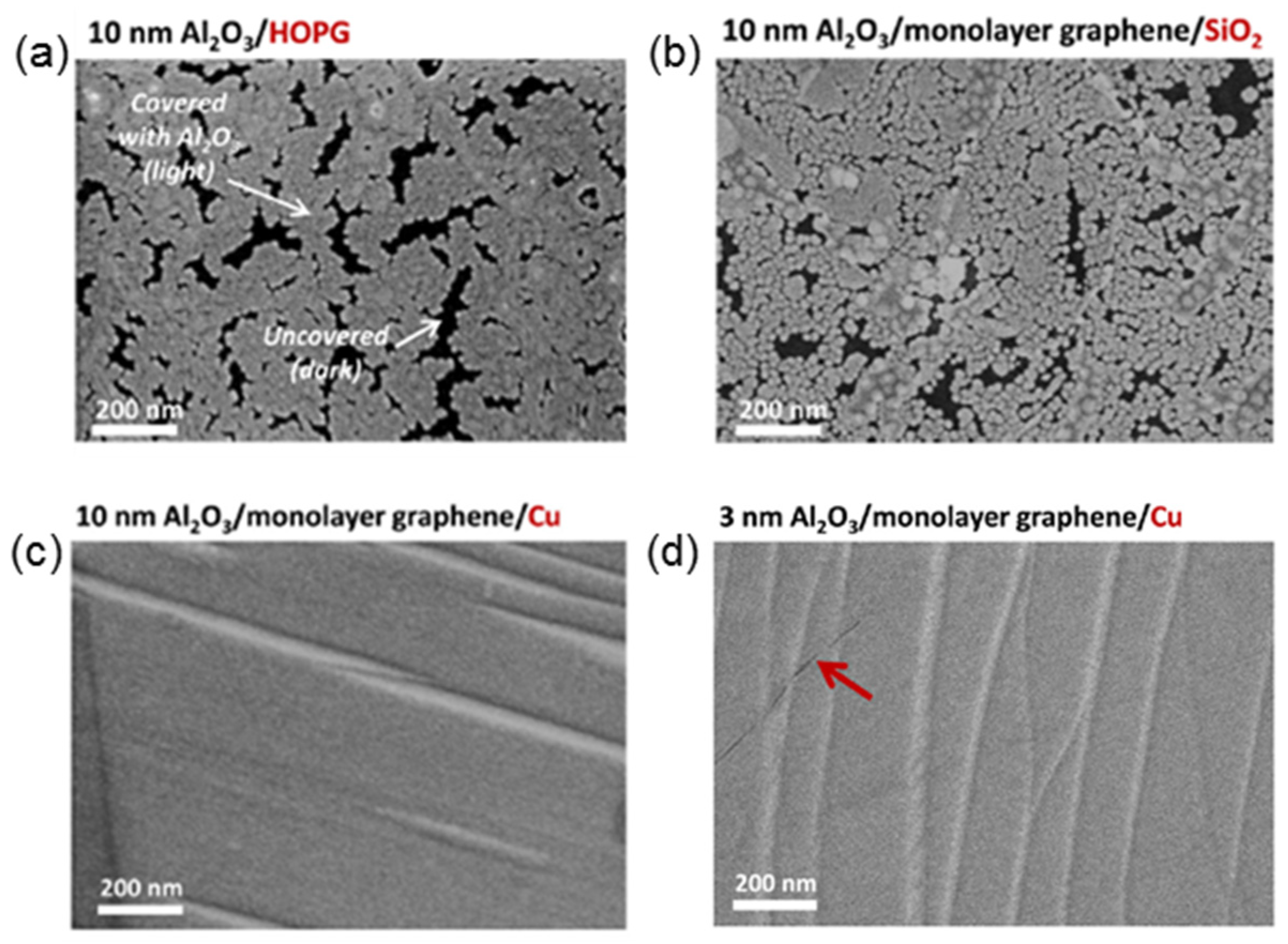
When an AD process is carried out on graphene membrane, the underlying substrate can play an important role, because it determines the wettability degree of the graphene surface. This effect has been demonstrated by Dublak et al. [21] by performing ALD deposition of Al2O3 on three different kinds of graphene materials: highly oriented pyrolitic graphite (HOPG), 1 L graphene grown by CVD on a copper substrate, and 1 L CVD graphene transferred on a SiO2 substrate. Figure 4 shows the nucleation mode of the dielectric on the three systems. By performing a deposition process consisting of 100 cycles (in order to obtain a thickness lower than 10 nm) at a temperature of 80 °C, they found discontinuous coverage both on the HOPG (Figure 4a) and on 1 L graphene transferred on a SiO2 substrate (Figure 4b). Using the same ALD conditions, complete coverage on the entire area was instead observed in the case of 1 L graphene residing on the native metal substrate (Cu in this case) (Figure 4c). Uniform coverage was obtained even in the case of ultra-thin (~3 nm) deposited Al2O3 films, as shown in Figure 4d.
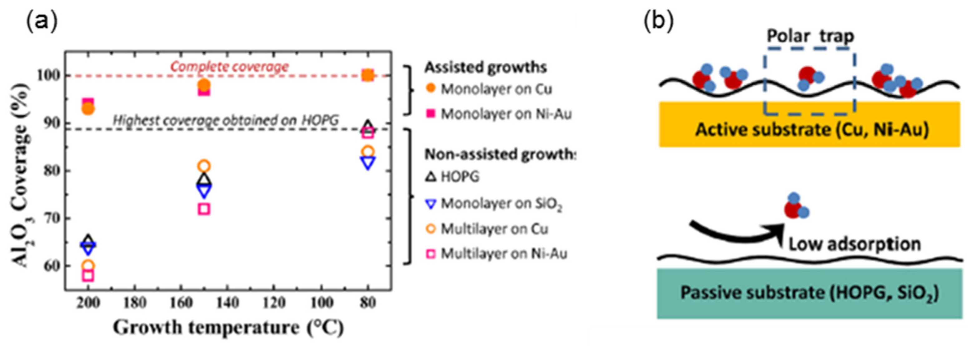
The authors also investigated the dependence of the Al2O3 coverage on the ALD deposition temperature (in the range from 80 °C to 200 °C) for 1 L and multilayer graphene supported by Cu or Ni-Au metal substrates, as well as for HOPG and 1 L graphene transferred onto SiO2 (Figure 5a). While a coverage percentage >90% was obtained on the metal-supported 1 L graphene in the considered temperature range, significantly lower coverage values were found for multilayers of graphene on the same metal substrates, with a similar temperature dependence to the case of HOPG and SiO2-supported 1 L graphene. Aside from Al2O3, other high-κ dielectrics (such as HfO2) grown by ALD showed similar improved ALD growth on the 1 L graphene and Cu system.
This strongly improved ALD growth was due to the partial transparency of 1 L graphene to the electrostatic fields generated by the polar traps at the graphene/metal interface [23,24,25,63]. Such polar sites are a consequence of charge transfer phenomena between the graphene and metal due to their work function difference and also the crystal and bond distortion. The electrostatic effect of polar traps causes enhanced adsorption of the water molecules (used as a co-reactant in the thermal ALD process) on the metal-supported 1 L graphene (Figure 5b, upper panel), resulting in improved nucleation of the high-κ dielectric and, consequently, of the surface coverage. Clearly, the transparency to electrostatic fields decreases with an increasing number of graphene layers, thus explaining the poor ALD coverage on multilayer graphene on the same metal substrates. Furthermore, the lack of these polar traps at the 1 L graphene/SiO2 interface or in HOPG results in low adsorption of the precursor molecules (as illustrated in Figure 5b, lower panel).
Using similar deposition parameters, Aria et al. [53] also reported a high coverage level of Al2O3 by ALD on 1 L graphene/Cu. In particular, they explored in detail the impact of the different deposition parameters (temperature, precursor pulse time, and number of ALD cycles) on the uniformity of the high-κ films. As an example, Figure 6 shows the evolution of Al2O3 coverage on 1 L graphene/Cu (a) with an increasing cycle number from 12 cycles (b) to 100 cycles (c) at a temperature of 200 °C.
The early-stage nucleation of high-κ dielectrics on graphene/Cu was studied by Bayer et al. [64] using scanning transmission electron microscopy (STEM) in the high-angle annular dark field (HAADF) mode. In particular, they investigated the nucleation mode of HfO2 considering the initial 16 deposition cycles. They proposed Volmer–Weber nucleation mechanism, which involves the initial island formation and the following coalescence of the islands toward the closing of the layer. Furthermore, they found a different HfO2 nucleation density between the 1 L and 2 L graphene regions. On the 1 L graphene, it was possible to observe by STEM the initial nuclei of the HfO2 layer, whereas on the 2 L region, the nucleation phenomena were sparsely distributed. Such a difference further confirms the screened substrate effect in the 2 L regions.
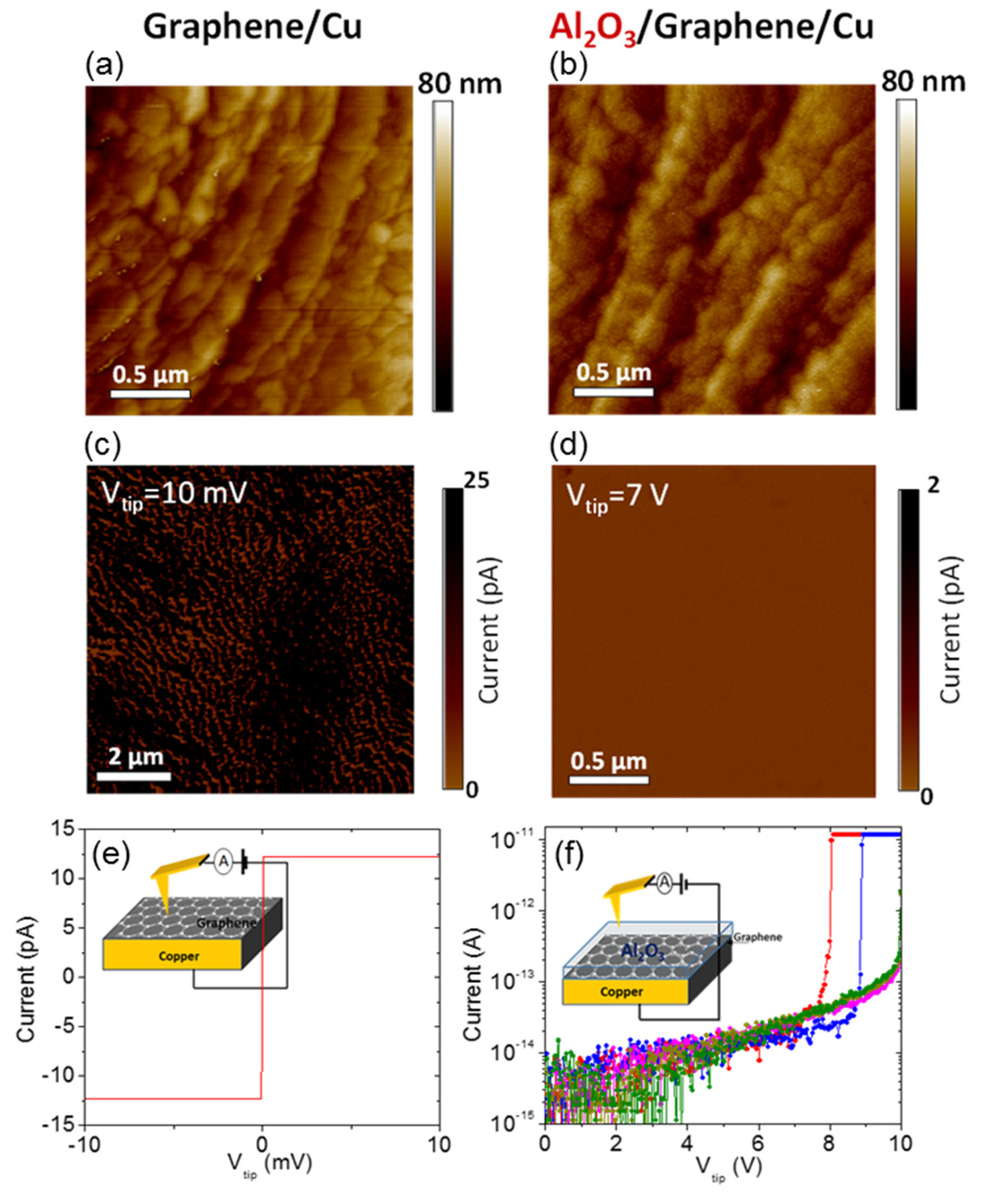
The electrical insulating properties of thin high-κ dielectrics deposited on metal-supported graphene can be studied with the Conductive Atomic Force Microscopy (C-AFM) technique [65,66]. Figure 7a,b shows the surface morphologies of the as-grown 1 L graphene/Cu and after ALD of a 10-nm thick Al2O3 layer at a temperature of 250 °C. The high roughness of the copper substrate made it difficult to evaluate the morphology of the deposited Al2O3 and the coverage fraction. Figure 7c,d shows the corresponding current maps of 1 L graphene/Cu and of Al2O3 (10 nm)/1 L graphene/Cu, acquired using the experimental configuration depicted in the insets of Figure 7e,f. As expected, the conductivity map of the bare graphene/Cu (Figure 7c) exhibited high current flow on the entire investigated area, even for a very low bias (VTip = 10 mV) applied to the tip. Conversely, the current map acquired on the Al2O3 deposited on the graphene/Cu showed optimal and uniform insulator behavior on the entire investigated surface up to an applied voltage of VTip = 7 V. No spots associated with the local current flow could be observed, and this is an indication of uniform nucleation and ALD growth of the dielectric on the 1 L graphene/Cu system. Figure 7e displays a typical current–voltage (I-VTip) characteristic measured by C-AFM on the bare 1 L graphene/Cu sample, which exhibits the expected Ohmic conduction behavior with very low resistance, whereas Figure 7f reports the local I-VTip curves acquired on the deposited 10 nm Al2O3 on 1 L graphene/Cu, showing negligible current flow through the insulating layer for tip bias values VTip < 7 V and the abrupt rise in the current, corresponding to a local dielectric breakdown at larger bias values.
3.2. ALD on Epitaxial Graphene on SiC
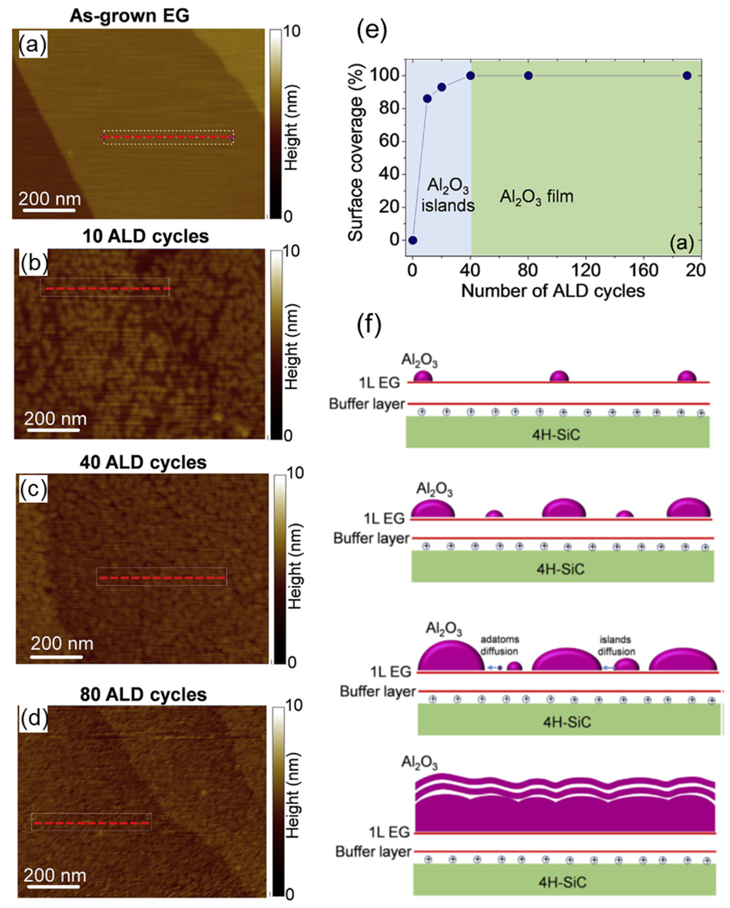
Epitaxial graphene (EG) grown by high-temperature (1600–2000 °C) thermal decomposition of the SiC(0001) surface typically consists of 1 L graphene on a large percentage of the surface area and 2 L or 3 L graphene regions especially localized at the step edges of the SiC surface terraces [67,68]. ALD growth of high-κ dielectrics, such as Al2O3 and HfO2, on epitaxial graphene (EG) on SiC typically results in inhomogeneous coverage [69,70], mainly on the 2 L or regions with few layers. However, by using highly homogeneous epitaxial graphene consisting of a monolayer for 98% of the surface and a bilayer for the remaining 2%, very uniform and pinhole-free Al2O3 layers have been obtained by direct thermal ALD at 250 °C without any seeding layer or pre-functionalization [26]. On the other hand, very inhomogeneous ALD coverage has been observed under identical ALD conditions on monolayer graphene transferred on a pristine SiC substrate. This demonstrates that the enhanced reactivity of the epitaxial graphene towards ALD precursors is not related to the SiC substrate but rather to the peculiar EG/SiC interface. Ab initio density functional theory (DFT) calculations demonstrated enhanced adsorption energy for the water molecules (ALD precursor) on 1 L graphene, depending on the n-type doping. Thus, the high doping induced by the buffer layer (between the EG and SiC substrate) on the EG was considered a possible origin of the excellent Al2O3 nucleation. The effectiveness of ALD nucleation has been demonstrated following the evolution of the surface morphology, starting from the as-grown EG surface (Figure 8a) and in the early deposition cycles (10, 20, and 40 cycles) [27] as shown in Figure 8b–d. A coverage level of >80% was observed already after 10 deposition cycles and 100% after 40 deposition cycles (Figure 8e). The evolution of ALD nucleation during the first few cycles is schematically depicted in Figure 8f, which displays four consecutive steps with an increasing number of ALD cycles (from top to bottom): (1) the formation of the first nuclei on the 1 L EG surface, (2) the increase of pre-existent nuclei and the further nucleation on bare EG, (3) diffusion and coalescence of the islands, and (4) the formation of a complete layer of dielectrics on graphene.
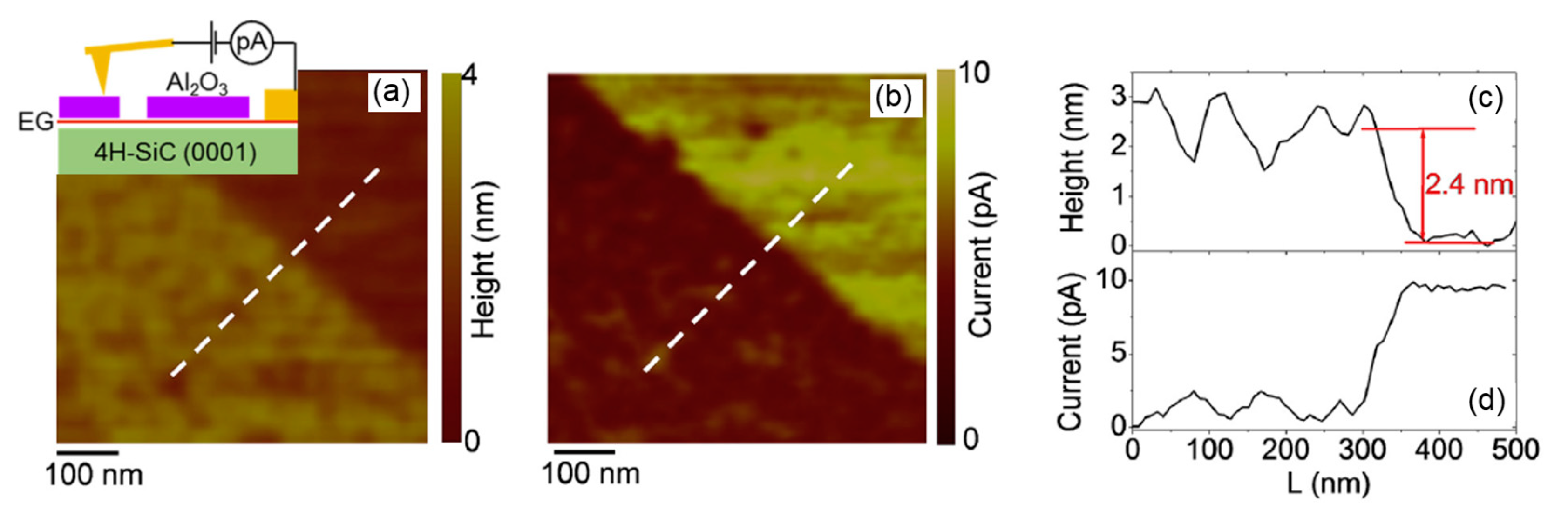
Figure 9 shows the morphology (a) and current map (b) acquired by C-AFM on a scratch of the Al2O3, demonstrating continuous ultrathin layers (~2.4 nm) of dielectrics with optimal insulator behavior (c,d). The slight fluctuations of the injected current, observable by the current map, through the ultra-thin dielectric layer are related to local changes in the surface roughness, as can be deduced from the comparison between the height and current line profiles. The obtained results have an important impact on devices exploiting epitaxial graphene.
3.3. ALD on Exfoliated MoS2 on Gold
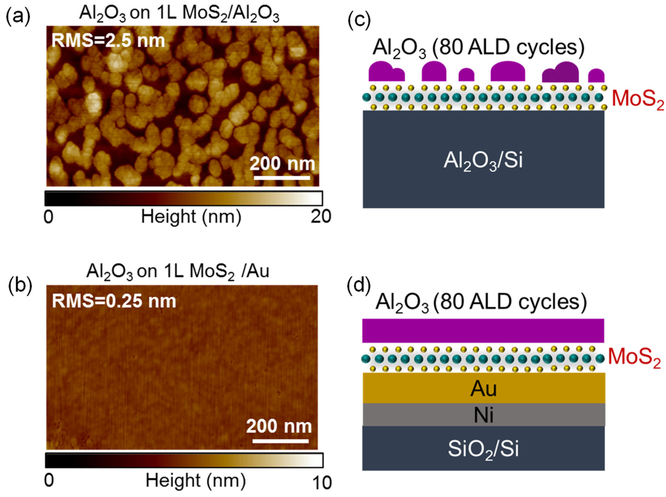
More recently, the direct thermal ALD of an ultra-thin and pinhole-free Al2O3 layer has been demonstrated on monolayer (1 L) MoS2 residing on a gold substrate [22]. During the last few years, several research groups have investigated mechanical exfoliation on gold as an effective way to separate large-area (cm2) 1 L MoS2 membranes from bulk molybdenite crystals by exploiting the strong S-Au interactions [71,72,73]. Furthermore, the exfoliated membranes could be transferred from gold to insulating substrates, demonstrating electrical and optical properties comparable to the best-quality MoS2 crystals [71,74]. Recently, Schilirò et al. [22] compared the thermal ALD of Al2O3 on 1 L MoS2 residing on gold and on 1 L MoS2, transferred on an insulating Al2O3 substrate. Using identical ALD conditions, inhomogeneous ALD coverage by Al2O3 islands was obtained in the case of the 1 L MoS2/Al2O3/Si (see Figure 10a). In contrast, pinhole-free Al2O3 and a flat morphology were observed on the 1 L MoS2/Au system (see Figure 10b). The authors illustrated the two different growth modes in Figure 10c,d for ALD-Al2O3 on 1 L MoS2/Al2O3/Si and on 1 L MoS2/Au, respectively. They found that the ALD nucleation on 1 L MoS2/Au was favored from the early stages of the process, with the Al2O3 surface coverage increasing from ~50% (after only 10 ALD cycles) to >90% (after 40 cycles). Interestingly, less uniform Al2O3 coverage was observed in the bilayer and multilayer MoS2 regions. The close similarity of the observed behavior to the case of 1 L graphene/Cu suggested that the improved reactivity of Au-supported 1 L MoS2 toward the ALD precursors could be attributed to the partial transparency of 1 L MoS2 to the electrostatic field generated by charges at the interface with the gold substrate. Furthermore, the strong interaction between MoS2 and Au was found to be responsible for the significant tensile strain and p-type doping of 1 L MoS2, which were relaxed by increasing the number of MoS2 layers [74]. Hence, these effects of the MoS2/Au interaction can also play a role in the enhanced nucleation in the early stages of ALD processes.
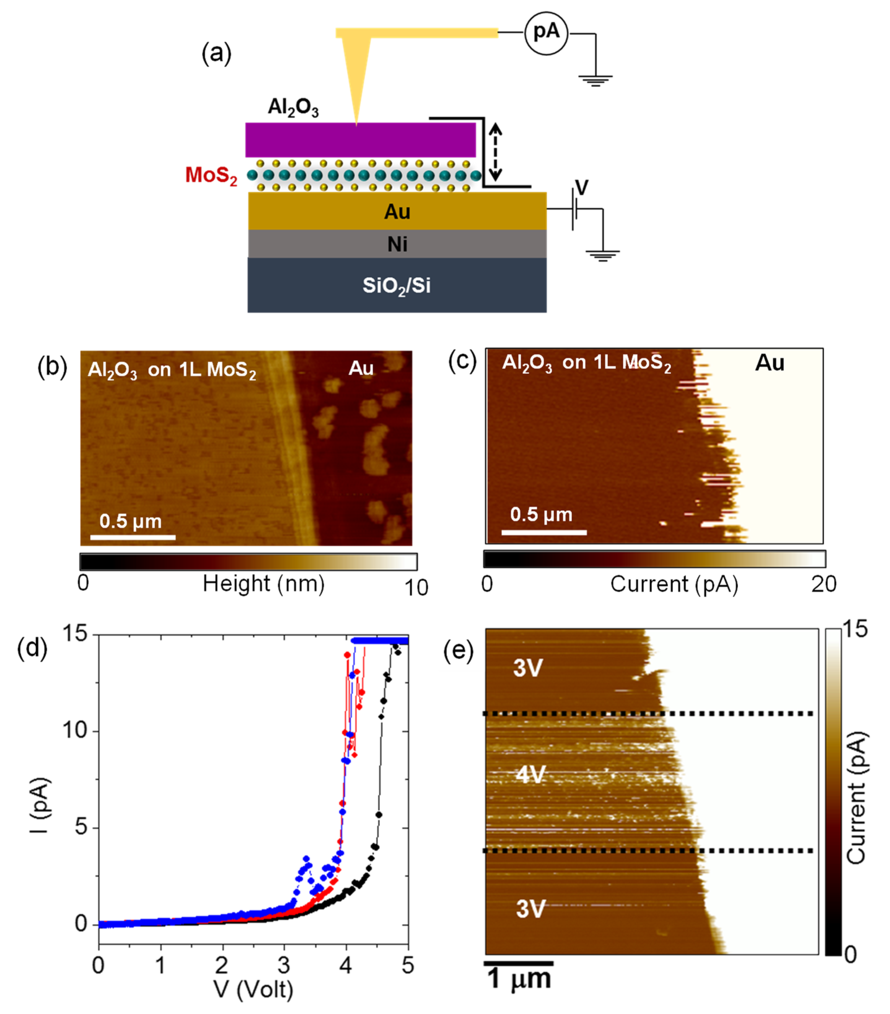
The thickness and the insulating properties of the uniform Al2O3 layer on MoS2/Au were also evaluated by C-AFM measurements according the schematic in Figure 11a. A 3.6-nm thickness of the Al2O3 on 1 L MoS2 was evaluated from the morphological map (Figure 11b), whereas the good insulating behavior of the deposited high-κ material was confirmed by the current map in Figure 11c, collected at a bias of 3 V between the tip and the gold substrate. Furthermore, the current–voltage (I–V) characteristics displayed in Figure 11d show a low leakage current of up to 3 V and a rapid increase in the current at bias values in the range of 3.7–4.5 V, associated with the localized breakdown behavior. These breakdown voltage (VBD) values correspond to breakdown electric fields (EBD = VBD/tox) in the range from ~10 to ~12 MV/cm. The localized behavior of the breakdown was also confirmed by the current map in Figure 11e, illustrating the changes in the leakage current spatial distribution by increasing the bias from 3 V to 4 V and then decreasing it back to 3 V. The appearance of localized breakdown spots is clearly visible in the current map region at 4 V of applied bias.
4. Challenges for Applications
The above-discussed substrate-enhanced ALD provides a unique way to obtain uniform and compact films of high-κ dielectrics with very good insulating properties directly on the pristine surface of 1 L graphene or MoS2. However, some challenges need to be faced for the application of the obtained high-κ/2D material stacks in electronic devices. Firstly, the substrate-enhanced ALD growth is observed especially on the monolayers of these 2D materials, whereas less uniform and compact films are typically obtained on the bilayer of the multilayers. Although graphene CVD on copper and the sublimation growth of epitaxial graphene on SiC(0001) have been widely investigated in the last decade, but obtaining uniform 1 L graphene on a large area still remains a challenge. In fact, a small percentage (1–2%) of the copper or SiC surface, typically corresponding to surface defects in the crystals, is covered by 2 L or a few layers of graphene. In the case of MoS2 exfoliated from the bulk crystal on a gold substrate, the obtained membrane is mostly composed of monolayers, with a significant fraction being 2 L or multilayer regions. As a matter of fact, even the presence of few percent of areas with poor-quality high-κ films represents a critical point for some device applications, such as field effect transistors or vertical hot electron transistors. Hence, further optimization of graphene and MoS2 synthesis methods to achieve full monolayer coverage will be crucial to take full benefit of the substrate-enhanced ALD growth.
A second key challenge to be addressed will be the development of reliable procedures for the integration of the high-κ/2D material stacks in electronic devices. In fact, while the ALD-grown dielectrics on EG/SiC(0001) can be immediately employed for the fabrication of top-gated field effect transistors, the transfer of the high-κ/2D material stacks to an insulating or semiconductor substrate is required in the case of metal-supported 2D materials.
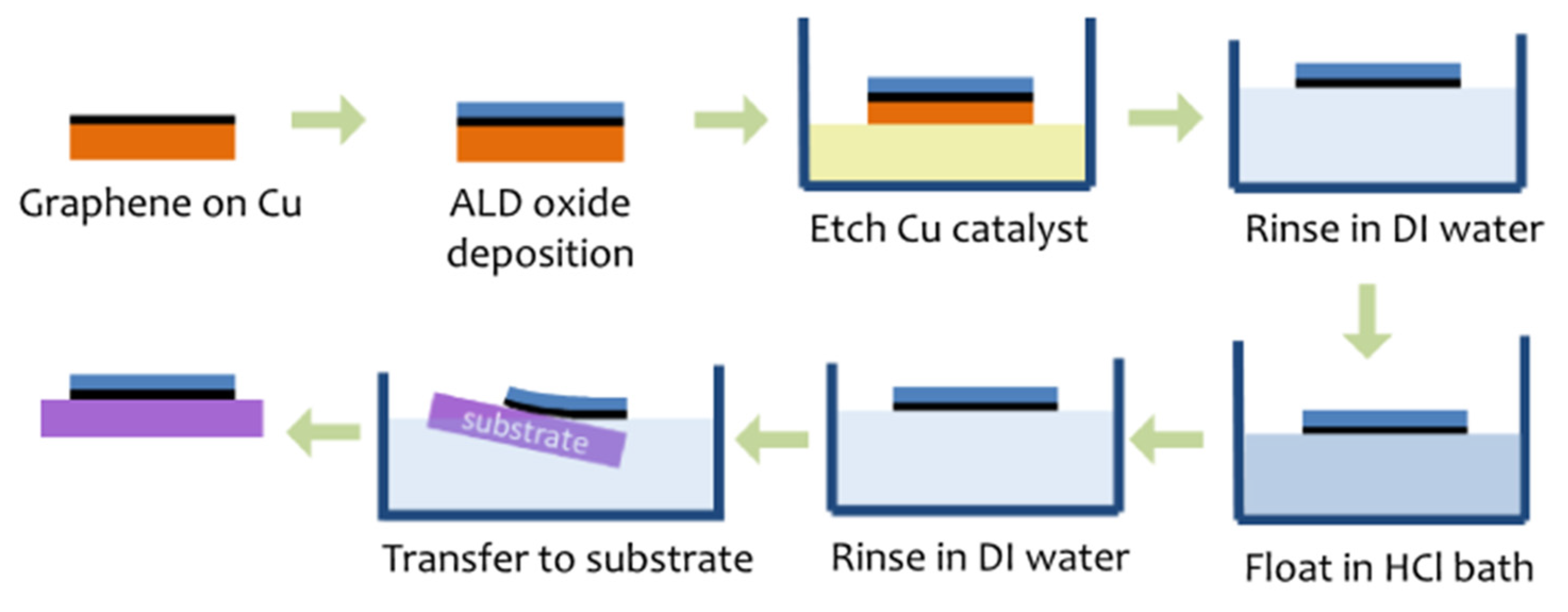
Recently, Cabrero-Vilatela et al. [75] also adopted the transfer procedure typically used for CVD-grown graphene on copper in the case of graphene coated by ALD-deposited Al2O3. As schematically illustrated in Figure 12, after direct ALD of the oxide on 1 L graphene/Cu, a poly-methyl methacrylate (PMMA) film was spin-coated on the oxide surface in order to protect the stack during the handling process. Therefore, the copper layer was removed by an etching solution and, after a series of rinses in DI water, the PMMA/Al2O3/graphene was transferred on the final substrate (SiO2/Si). The polymer support was finally removed by solvents.
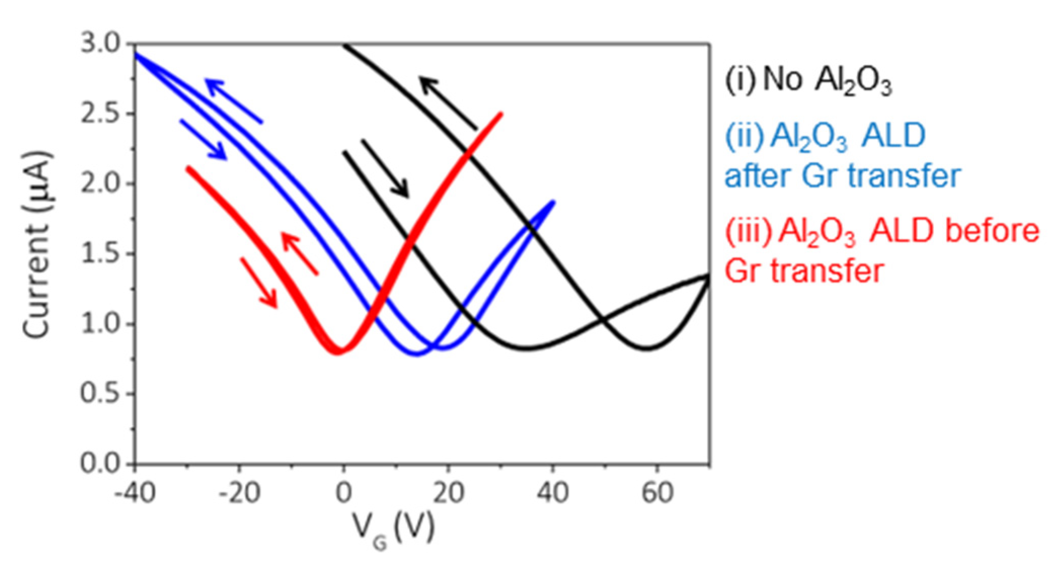
The same authors demonstrated a beneficial effect of the Al2O3 encapsulation of 1 L graphene/Cu on the final electrical performance of the graphene devices. Figure 13 shows the comparison of the transfer characteristics (ID-VG) of three different kinds of back-gated field effect transistors on a SiO2/Si substrate, fabricated using (1) graphene monolayers without Al2O3 on top (no Al2O3), (2) graphene monolayers with Al2O3 deposited after being transferred onto SiO2 (Al2O3 ALD after transfer), and (3) graphene monolayers with Al2O3 deposited before the transfer (Al2O3 ALD before transfer). It is noteworthy that the third approach guarantees both very low doping of graphene (i.e., a charge neutrality point very close to VG = 0 V) and reduced hysteresis of the characteristics, which are attributable to the significantly reduced charges at the interface. These improved electrical performances have been correlated to the reduced contaminations at the Al2O3/graphene interface, since the direct contact between graphene and PMMA is avoided in this case. In this regard, a double application of the Al2O3 layer deposited by ALD on the graphene on copper prior to the transfer process to SiO2 substrates has been proposed.
Aside from working as a protective layer for graphene during the transfer from copper and for passivation of the back-gated graphene transistors, the deposited high-κ films can be exploited as active layers (e.g., as dielectrics of top-gated field transistors or as a base collector barrier in graphene base hot electron transistors (GBHETs)). In this respect, the most crucial issue is the optimization of handling procedures to avoid damage or cracking of the high-κ/graphene stack during the transfer.
Similarly, the transfer of the dielectric/MoS2 stack from Au to an insulating substrate is mandatory for the field effect transistor applications of this system. To date, several authors demonstrated the transfer of large-area 1 L MoS2 exfoliated on Au to insulating substrates (using very similar methods to those used for CVD-grown graphene on copper), and excellent electronic and optical quality has been shown for the transferred 1 L MoS2 membranes [72,76]. However, the transfer of Al2O3-coated 1 L MoS2 from Au to other substrates has not been reported so far. The transfer from the metal substrate is not required for other recently investigated devices, such as MoS2 memristors [77], exploiting the properties of Au-supported 1 L MoS2 membranes for non-volatile memory applications.
5. Conclusions
The integration of uniform and ultra-thin high-κ dielectrics on 2D materials is a challenge for future electronic and sensing applications in these systems. In fact, the seed layer and pre-functionalization approaches typically employed to promote ALD nucleation on 2D materials presents both advantages and disadvantages, and direct ALD growth remains highly desirable. This paper provided a detailed review of the literature reports on the direct ALD of uniform high-κ dielectric films on monolayer graphene and MoS2, driven by the interaction with the underlying substrates. In the case of CVD 1 L graphene on copper, the enhancement of ALD nucleation was correlated with the electrostatic effect of polar traps (at the graphene/metal interface) on the adsorption of the water precursor. For 1 L epitaxial graphene on SiC(0001), a similar electrostatic effect happens due to the positive charges at the interface between the buffer layer and the substrate, which cause n-type doping of the graphene and its enhanced reactivity toward ALD precursors. Finally, in the case of 1 L MoS2 exfoliated on gold substrate, the improvement in ALD growth is explained by the combined effect of electrostatic charges at the interface and of the tensile strain induced on the 2D material by the gold. Hence, opportunely choosing the substrate, excellent ALD coverage, and optimal structural and insulating properties of the high-κ layers can be obtained on 2D materials. For all these systems, the electrical insulating properties of the grown high-κ dielectrics have been examined. Finally, the open issues and challenges for applications of these high-κ/2D material systems have been thoroughly discussed.
Author Contributions
Writing—original draft preparation, E.S.; writing—review and editing, F.G., R.L.N. and F.R.; supervision, F.G.; funding acquisition, F.G. and F.R. All authors have read and agreed to the published version of the manuscript.
Funding
This work was funded in part by MUR in the framework of the FlagERA-JTC 2019 project ETMOS. E.S. acknowledges the PON project EleGaNTe (ARS01_01007) funded by MUR for financial support.
Institutional Review Board Statement
Not applicable.
Informed Consent Statement
Not applicable.
Data Availability Statement
The data that support the findings of this study are available from the corresponding author upon reasonable request.
Acknowledgments
The authors want to acknowledge P. Fiorenza, G. Greco, S. Di Franco (CNR-IMM, Catania, Italy), S.E. Panasci (CNR-IMM Catania and University of Catania, Italy), M. Cannas, M. Gelardi, S. Agnello (University of Palermo, Italy), R. Yakimova, and I. Shtepliuk (Linkoping University, Sweden) for useful discussions and participation in some of the experiments reported in this review paper.
Conflicts of Interest
The authors declare no conflict of interest.
References
- Du, X.; Skachko, I.; Barker, A.; Aandrei, E.Y. Approaching ballistic transport in suspended graphene. Nat. Nanotechnol. 2008, 3, 491. [Google Scholar] [CrossRef] [PubMed] [Green Version]
- Giannazzo, F.; Sonde, S.; Lo Nigro, R.; Rimini, E.; Raineri, V. Mapping the Density of Scattering Centers Limiting the Electron Mean Free Path in Graphene. Nano Lett. 2011, 11, 4612–4618. [Google Scholar] [CrossRef] [PubMed]
- Lin, Y.-M.; Dimitrakopoulos, C.; Jenkins, K.A.; Farmer, D.B.; Chiu, H.-Y.; Grill, A.; Avouris, P. 100-GHz Transistors from Wafer-Scale Epitaxial Graphene. Science 2010, 327, 662. [Google Scholar] [CrossRef] [Green Version]
- Moon, J.S.; Curtis, D.; Hu, M.; Wong, D.; McGuire, C.; Campbell, P.M.; Jernigan, G.; Tedesco, J.L.; VanMil, B.; Myers-Ward, R.; et al. Epitaxial-Graphene RF Field-Effect Transistors on Si-Face 6H-SiC Substrates. IEEE Electron Device Lett. 2009, 30, 650–652. [Google Scholar] [CrossRef]
- Liu, H.; Neal, A.T.; Ye, P.D. Channel Length Scaling of MoS2 MOSFETs. ACS Nano 2012, 6, 8563–8569. [Google Scholar] [CrossRef] [Green Version]
- Liu, Y.; Guo, J.; Wu, Y.; Zhu, E.; Weiss, N.O.; He, Q.; Wu, H.; Cheng, H.-C.; Xu, Y.; Shakir, I.; et al. Pushing the Performance Limit of Sub-100 nm Molybdenum Disulfide Transistors. Nano Lett. 2016, 16, 6337–6342. [Google Scholar] [CrossRef] [PubMed]
- Radisavljevic, B.; Radenovic, A.; Brivio, J.; Giacometti, V.; Kis, A. Single-layer MoS2 transistors. Nat. Nanotechnol. 2011, 6, 147–150. [Google Scholar] [CrossRef]
- Kim, S.; Konar, A.; Hwang, W.S.; Lee, J.H.; Lee, J.; Yang, J.; Jung, C.; Kim, H.; Yoo, J.B.; Choi, J.Y.; et al. High-mobility and low-power thin-film transistors based on multilayer MoS2 crystals. Nat. Commun. 2012, 3, 1011. [Google Scholar] [CrossRef] [PubMed] [Green Version]
- Mak, K.F.; Lee, C.; Hone, J.; Shan, J.; Heinz, T.F. Atomically Thin MoS2: A New Direct-Gap Semiconductor. Phys. Rev. Lett. 2010, 105, 136805. [Google Scholar] [CrossRef] [Green Version]
- Splendiani, A.; Sun, L.; Zhang, Y.; Li, T.; Kim, J.; Chim, C.-Y.; Galli, G.; Wang, F. Emerging Photoluminescence in Monolayer MoS2. Nano Lett. 2010, 10, 1271–1275. [Google Scholar] [CrossRef] [PubMed]
- Reddy, D.; Register, L.F.; Carpenter, G.D.; Banerjee, S.K. Graphene Field-Effect Transistors. J. Phys. D Appl. Phys. 2011, 45, 019501. [Google Scholar] [CrossRef]
- Echtermeyer, T.J.; Lemme, M.C.; Baus, M.; Szafranek, B.N.; Geim, A.K.; Kurz, H. Non-volatile switching in graphene field effect devices. IEEE Electron Device Lett. 2008, 29, 29952–29954. [Google Scholar] [CrossRef] [Green Version]
- Fisichella, G.; Lo Verso, S.; Di Marco, S.; Vinciguerra, V.; Schilirò, E.; Di Franco, S.; Lo Nigro, R.; Roccaforte, F.; Zurutuza, A.; Centeno, A.; et al. Advances in the fabrication of graphene transistors on flexible substrates. Beilstein J. Nanotechnol. 2017, 8, 467–474. [Google Scholar] [CrossRef] [PubMed] [Green Version]
- Liu, H.; Ye, P.D. MoS2 Dual-Gate MOSFET With Atomic-Layer-Deposited Al2O3 as Top-Gate Dielectric. IEEE Electron Device Lett. 2011, 33, 546–548. [Google Scholar] [CrossRef] [Green Version]
- Giannazzo, F.; Greco, G.; Roccaforte, F.; Sonde, S.S. Vertical Transistors Based on 2D Materials: Status and Prospects. Crystals 2018, 8, 70. [Google Scholar] [CrossRef] [Green Version]
- Giannazzo, F. Engineering 2D heterojunctions with dielectrics. Nat. Electron. 2019, 2, 54. [Google Scholar] [CrossRef]
- Giannazzo, F.; Fisichella, G.; Greco, G.; Schilirò, E.; Deretzis, I.; Lo Nigro, R.; La Magna, A.; Roccaforte, F.; Iucolano, F.; Lo Verso, S.; et al. Cordier, Fabrication and Characterization of Graphene Heterostructures with Nitride semiconductors for High Frequency Vertical Transistors. Phys. Status Solidi 2017, 215, 1700653. [Google Scholar] [CrossRef]
- Giannazzo, F.; Greco, G.; Schilirò, E.; Lo Nigro, R.; Deretzis, I.; La Magna, A.; Roccaforte, F.; Iucolano, F.; Ravesi, S.; Frayssinet, E.; et al. High-performance graphene/AlGaN/GaN schottky junctions for hot electron transistors. ACS Appl. Electron. Mater. 2019, 1, 2342–2354. [Google Scholar] [CrossRef]
- Mehr, W.; Dabrowski, J.; Scheytt, J.C.; Lippert, G.; Xie, Y.H.; Lemme, M.C.; Ostling, M.; Lupina, G. Vertical Graphene Base Transistor. IEEE Electron Device Lett. 2012, 33, 691–693. [Google Scholar] [CrossRef] [Green Version]
- Bae, T.-E.; Kim, H.; Jung, J.; Cho, W.-J. Fabrication of high-performance graphene field-effect transistor with solution-processed Al2O3 sensing membrane. Appl. Phys. Lett. 2014, 104, 153506. [Google Scholar] [CrossRef]
- Dlubak, B.; Kidambi, P.R.; Weatherup, R.S.; Hofmann, S.; Robertson, J. Substrate-assisted nucleation of ultra-thin dielectric layers on graphene by atomic layer deposition. Appl. Phys. Lett. 2012, 100, 173113. [Google Scholar] [CrossRef]
- Schilirò, E.; Lo Nigro, R.; Panasci, S.E.; Agnello, S.; Cannas, M.; Gelardi, F.M.; Roccaforte, F.; Giannazzo, F. Direct Atomic Layer Deposition of Ultrathin Aluminum Oxide on Monolayer MoS2 Exfoliated on Gold: The Role of the Substrate. Adv. Mater. Interfaces 2021, 8, 2101117. [Google Scholar] [CrossRef]
- Pollard, A.J.; Perkins, E.W.; Smith, N.A.; Saywell, A.; Goretzki, G.; Phillips, A.G.; Argent, S.P.; Sachdev, H.; Müller, F.; Hüfner, S.; et al. Supramolecular Assemblies Formed on an Epitaxial Graphene Superstructure. Angew. Chem. Int. Ed. 2010, 49, 1794. [Google Scholar] [CrossRef] [PubMed]
- Zhang, H.; Sun, J.; Low, T.; Zhang, L.; Pan, Y.; Liu, Q.; Mao, J.; Zhou, H.; Guo, H.; Du, S.; et al. Assembly of iron phthalocyanine and pentacene molecules on a graphene monolayer grown on Ru(0001). Phys. Rev. B 2011, 84, 245436. [Google Scholar] [CrossRef] [Green Version]
- Rafiee, J.; Mi, X.; Gullapalli, H.; Thomas, A.V.; Yavari, F.; Shi, Y.; Ajayan, P.M.; Koratkar, N.A. Wetting transparency of graphene. Nat. Mater. 2012, 11, 217–222. [Google Scholar] [CrossRef] [PubMed]
- Schilirò, E.; Lo Nigro, R.; Roccaforte, F.; Deretzis, I.; La Magna, A.; Armano, A.; Agnello, S.; Pecz, B.; Ivanov, I.G.; Yakimova, R.; et al. Seed-Layer-Free Atomic Layer Deposition of Highly Uniform Al2O3 Thin Films onto Monolayer Epitaxial Graphene on Silicon Carbide. Adv. Mater. Interfaces 2019, 6, 1900097. [Google Scholar] [CrossRef]
- Schilirò, E.; Lo Nigro, R.; Panasci, S.E.; Gelardi, F.M.; Agnello, S.; Yakimova, R.; Roccaforte, F.; Giannazzo, F. Aluminum oxide nucleation in the early stages of atomic layer deposition on epitaxial graphene. Carbon 2020, 169, 172–181. [Google Scholar] [CrossRef]
- Vervuurt, R.H.J.; Kessels, W.M.M.; Bol, A.A. Atomic Layer Deposition for Graphene Device Integration. Adv. Mater. Interfaces 2017, 4, 1700232. [Google Scholar] [CrossRef] [Green Version]
- Kim, H.G.; Lee, H.-B.-R. Atomic Layer Deposition on 2D Materials. Chem. Mater. 2017, 29, 3809–3826. [Google Scholar] [CrossRef]
- Giannazzo, F.; Schilirò, E.; Lo Nigro, R.; Roccaforte, F.; Yakimova, R. Atomic Layer Deposition of High-k Insulators on Epitaxial Graphene: A Review. Appl. Sci. 2020, 10, 2440. [Google Scholar] [CrossRef] [Green Version]
- Oviroh, P.O.; Akbarzadeh, R.; Pan, D.; Coetzee, R.A.M.; Jen, T.-C. New development of atomic layer deposition: Processes, methods and applications. Sci. Technol. Adv. Mater. 2019, 20, 465–496. [Google Scholar] [CrossRef] [Green Version]
- Park, T.; Kim, H.; Leem, M.; Ahn, W.; Choi, S.; Kim, J.; Uh, J.; Kwon, K.; Jeong, S.-J.; Park, S.; et al. Atomic layer deposition of Al2O3 on MoS2, WS2, WSe2, and h-BN: Surface coverage and adsorption energy. RSC Adv. 2017, 7, 884–889. [Google Scholar] [CrossRef] [Green Version]
- Cheng, L.; Qin, X.; Lucero, A.T.; Azcatl, A.; Huang, J.; Wallace, R.M.; Cho, K.; Kim, J. Atomic Layer Deposition of a High-k Dielectric on MoS2 Using Trimethylaluminum and Ozone. ACS Appl. Mater. Interfaces 2014, 6, 11834–11838. [Google Scholar] [CrossRef] [PubMed] [Green Version]
- Wang, X.; Tabakman, S.M.; Dai, H. Atomic Layer Deposition of Metal Oxides on Pristine and Functionalized Graphene. J. Am. Chem. Soc. 2008, 130, 8152. [Google Scholar] [CrossRef] [Green Version]
- Shin, W.C.; Kim, T.Y.; Sul, O.; Cho, B.J. Seeding atomic layer deposition of high-k dielectric on graphene with ultrathin poly(4-vinylphenol) layer for enhanced device performance and reliability. Appl. Phys. Lett. 2012, 101, 033507. [Google Scholar] [CrossRef]
- Wirtz, C.; Hallam, T.; Cullen, C.P.; Berner, N.C.; O’Brien, M.; Marcia, M.; Hirsch, A.; Duesberg, G.S. Atomic layer deposition on 2D transition metal chalcogenides: Layer dependent reactivity and seeding with organic ad-layers. Chem. Commun. 2015, 51, 16553. [Google Scholar] [CrossRef] [PubMed] [Green Version]
- Fallahazad, B.; Lee, K.; Lian, G.; Kim, S.; Corbet, C.; Ferrer, D.; Colombo, L.; Tutuc, E. Scaling of Al2O3 dielectric for graphene field-effect transistors. Appl. Phys. Lett. 2012, 100, 093112. [Google Scholar] [CrossRef]
- Guo, T.; Wu, H.; Su, X.; Guo, B.; Liu, C. Surface functionalization toward top-gated monolayer MoS2 field-effect transistors with ZrO2/Al2O3 as composite dielectrics. J. Alloy. Compd. 2021, 871, 159116. [Google Scholar] [CrossRef]
- Woo, W.J.; Oh, I.K.; Park, B.E.; Kim, Y.; Park, J.; Seo, S.; Song, J.-G.; Jung, H.; Kim, D.; Lim, J.H.; et al. Bi-layer high-k dielectrics of Al2O3/ZrO2 to reduce damage to MoS2 channel layers during atomic layer deposition. 2D Mater. 2019, 6, 015019. [Google Scholar] [CrossRef]
- Haodong, Z.; Arutchelvan, G.; Meersschaut, J.; Gaur, A.; Conard, T.; Bender, H.; Lin, D.; Asselberghs, I.; Heyns, M.; Radu, I.; et al. MoS2 Functionalization with a Sub-nm Thin SiO2 Layer for Atomic Layer Deposition of High-κ Dielectrics. Chem. Mater. 2017, 29, 6772–6780. [Google Scholar]
- Zhang, Y.; Qiu, Z.; Cheng, X.; Xie, H.; Wang, H.; Xie, X.; Yu, Y.; Liu, R. Direct growth of high-quality Al2O3 dielectric on graphene layers by low-temperature H2O-based ALD. J. Phys. D Appl. Phys. 2014, 47, 055106. [Google Scholar] [CrossRef]
- Fisichella, G.; Schilirò, E.; Di Franco, S.; Fiorenza, P.; Lo Nigro, R.; Roccaforte, F.; Ravesi, S.; Giannazzo, F. Interface Electrical Properties of Al2O3 Thin Films on Graphene Obtained by Atomic Layer Deposition with an in Situ Seedlike Layer. ACS Appl. Mater. Interfaces 2017, 9, 7761–7771. [Google Scholar] [CrossRef] [PubMed]
- Lin, Y.-S.; Cheng, P.-H.; Huang, K.-W.; Lin, H.-C.; Chen, M.-J. Atomic layer deposition of sub-10 nm high-K gate dielectrics on top-gated MoS2 transistors without surface functionalization. Appl. Surf. Sci. 2018, 443, 421–428. [Google Scholar] [CrossRef]
- Gong, F.; Luo, W.; Wang, J.; Wang, P.; Fang, H.; Zheng, D.; Guo, N.; Wang, J.; Luo, M.; Ho, J.C.; et al. High-Sensitivity Floating-Gate Phototransistors Based on WS2 and MoS2. Adv. Funct. Mater. 2016, 26, 6084–6090. [Google Scholar] [CrossRef]
- Lin, Y.M.; Jenkins, K.A.; Valdes-Garcia, A.; Small, J.P.; Farmer, D.B.; Avouris, P. Operation of Graphene Transistors at Gigahertz Frequencies. Nano Lett. 2009, 9, 422. [Google Scholar] [CrossRef] [Green Version]
- Lee, B.; Mordi, G.; Kim, M.J.; Chabal, Y.J.; Vogel, E.M.; Wallace, R.M.; Cho, K.J.; Colombo, L.; Kim, J. Characteristics of high-k Al2O3 dielectric using ozone-based atomic layer deposition for dual-gated graphene devices. J. Appl. Phys. Lett. 2010, 97, 043107. [Google Scholar] [CrossRef]
- Lee, J.; Lee, B.; Kim, J.; Cho, K. Ozone Adsorption on Graphene: Ab Initio Study and Experimental Validation. J. Phys. Chem. C 2009, 113, 14225. [Google Scholar] [CrossRef] [Green Version]
- Lee, B.; Park, S.Y.; Kim, H.C.; Cho, K.; Vogel, E.M.; Kim, M.J.; Wallace, R.M.; Kim, J. Conformal Al2O3 dielectric layer deposited by atomic layer deposition for graphene-based nanoelectronics. J. Appl. Phys. Lett. 2008, 92, 203102. [Google Scholar] [CrossRef]
- Azcatl, A.; Santosh, K.C.; Peng, X.; Lu, N.; McDonnell, S.; Qin, X.; de Dios, F.; Addou, R.; Kim, J.; Kim, M.J.; et al. HfO2 on UV-O3 Exposed Transition Metal Dichalcogenides: Interfacial Reactions Study. 2D Mater. 2015, 2, 014004. [Google Scholar] [CrossRef] [Green Version]
- Yang, J.; Kim, S.; Choi, W.; Park, S.H.; Jung, Y.; Cho, M.-H.; Kim, H. Improved Growth Behavior of Atomic-Layer-Deposited High-k Dielectrics on Multilayer MoS2 by Oxygen Plasma Pretreatment. ACS Appl. Mater. Interfaces 2013, 5, 4739–4744. [Google Scholar] [CrossRef] [PubMed]
- Nayfeh, O.M.; Marr, T.; Dubey, M. Impact of Plasma-Assisted Atomic-Layer-Deposited Gate Dielectric on Graphene Transistors. IEEE Electron Device Lett. 2011, 32, 473–475. [Google Scholar] [CrossRef]
- Lim, T.; Kim, D.; Ju, S. Direct deposition of aluminum oxide gate dielectric on graphene channel using nitrogen plasma treatment. Appl. Phys. Lett. 2013, 113, 013107. [Google Scholar] [CrossRef]
- Aria, A.I.; Nakanishi, K.; Xiao, L.; Braeuninger-Weimer, P.; Sagade, A.A.; Alexander-Webber, J.A.; Hofmann, S. Parameter Space of Atomic Layer Deposition of Ultrathin Oxides on Graphene. ACS Appl. Mater. Interfaces 2016, 8, 30564. [Google Scholar] [CrossRef]
- Kwak, I.; Kavrik, M.; Park, J.H.; Grissom, L.; Fruhberger, B.; Wong, K.T.; Kang, S.; Kummel, A.C. Low interface trap density in scaled bilayer gate oxides on 2D materials via nanofog low temperature atomic layer deposition. Appl. Surf. Sci. 2019, 463, 758–766. [Google Scholar] [CrossRef]
- Kitzmann, J.; Göritz, A.; Fraschke, M.; Lukosius, M.; Wenger, C.; Wolff, A.; Lupina, G. Perfluorodecyltrichlorosilane-based seed-layer for improved chemical vapour deposition of ultrathin hafnium dioxide films on graphene. Sci. Rep. 2016, 6, 29223. [Google Scholar] [CrossRef] [Green Version]
- Farmer, D.B.; Chiu, H.-Y.; Lin, Y.-M.; Jenkins, K.A.; Xia, F.; Avouris, P. Utilization of a Buffered Dielectric to Achieve High Field-Effect Carrier Mobility in Graphene Transistors. Nano Lett. 2009, 9, 4474. [Google Scholar] [CrossRef] [Green Version]
- Kim, S.; Nah, J.; Jo, I.; Shahrjerdi, D.; Colombo, L.; Yao, Z.; Tutuc, E.; Banerjee, S.K. Realization of a high mobility dual-gated graphene field-effect transistor with Al2O3 dielectric. Appl. Phys. Lett. 2009, 94, 062107. [Google Scholar] [CrossRef] [Green Version]
- Iraiwa, A.; Matsumura, D.; Kawarada, H. Effect of atomic layer deposition temperature on current conduction in Al2O3 films formed using H2O oxidant. J. Appl. Phys. 2016, 120, 084504. [Google Scholar]
- Fallahazad, B.; Kim, S.; Colombo, L.; Tutuc, E. Dielectric Thickness Dependence of Carrier Mobility in Graphene with HfO2 Top Dielectric. Appl. Phys. Lett. 2010, 97, 123105. [Google Scholar] [CrossRef] [Green Version]
- Zhao, P.; Khosravi, A.; Azcatl, A.; Bolshakov, P.; Mirabelli, G.; Caruso, E.; Hinkle, C.L.; Hurley, P.K.; Wallace, R.M.; Young, C.D. Evaluation of border traps and interface traps in HfO2/MoS2 gate stacks by capacitance–voltage analysis. 2D Mater. 2018, 5, 031002. [Google Scholar] [CrossRef] [Green Version]
- Zhou, P.; Yang, S.; Sun, Q.; Chen, L.; Wang, P.; Ding, S.; Zhang, D.W. Direct Deposition of Uniform High-k Dielectrics on Graphene. Sci. Rep. 2014, 4, 6448. [Google Scholar] [CrossRef] [Green Version]
- Dingemans, G.; van de Sanden, M.C.M.; Kessels, W.M.M. Influence of the Deposition Temperature on the c-Si Surface Passivation by Al2O3 Films Synthesized by ALD and PECVD. Electrochem. Solid-State Lett. 2010, 13, H76. [Google Scholar] [CrossRef] [Green Version]
- Roos, M.; Ku¨nzel, D.; Uhl, B.; Huang, H.H.; Brandao, O.; Hoster, H.E.; Gross, A.; Behm, R.J. Hierarchical Interactions and Their Influence upon the Adsorption of Organic Molecules on a Graphene Film. J. Am. Chem. Soc. 2011, 133, 9208. [Google Scholar] [CrossRef]
- Bayer, B.C.; Aria, A.I.; Eder, D.; Hofmann, S.; Meyer, J.C. Resolving the Nucleation Stage in Atomic Layer Deposition of Hafnium Oxide on Graphene. arXiv 2019, arXiv:1909.00712. [Google Scholar]
- Giannazzo, F.; Fisichella, G.; Greco, G.; Fiorenza, P.; Roccaforte, F. Conductive Atomic Force Microscopy: Applications in Nanomaterials; Lanza, M., Ed.; Wiley-VCH Verlag: Weinheim, Germany, 2017; Chapter 7; pp. 163–186. [Google Scholar]
- Sonde, S.; Giannazzo, F.; Raineri, V.; Yakimova, R.; Huntzinger, J.-R.; Tiberj, A.; Camassel, J. Electrical properties of the graphene/4H-SiC (0001) interface probed by scanning current spectroscopy. Phys. Rev. B 2009, 80, 241406(R). [Google Scholar] [CrossRef]
- Emtsev, K.V.; Bostwick, A.; Horn, K.; Jobst, J.; Kellogg, G.L.; Ley, L.; McChesney, J.L.; Ohta, T.; Reshanov, S.A.; Reohrl, J.; et al. Towards wafer-size graphene layers by atmospheric pressure graphitization of silicon carbide. Nat. Mater. 2009, 8, 203–207. [Google Scholar] [CrossRef]
- Giannazzo, F.; Deretzis, I.; La Magna, A.; Roccaforte, F.; Yakimova, R. Electronic transport at monolayer-bilayer junctions in epitaxial graphene on SiC. Phys. Rev. B 2012, 86, 235422. [Google Scholar] [CrossRef]
- Speck, F.; Ostler, M.; Rohrl, J.; Emtsev, K.V.; Hundhausen, M.; Ley, L.; Seyller, T. Atomic layer deposited aluminum oxide films on graphite and graphene studied by XPS and AFM. Phys. Status Solidi C 2010, 7, 398. [Google Scholar] [CrossRef]
- Robinson, J.A.; LaBella, M.; Trumbull, K.A.; Weng, X.; Cavelero, R.; Daniels, T.; Hughes, Z.; Hollander, M.; Fanton, M. Nucleation of Epitaxial Graphene on SiC(0001). ACS Nano 2010, 4, 2667. [Google Scholar] [CrossRef]
- Desai, S.R.; Madhvapathy, S.R.; Amani, M.; Kiriya, D.; Hettick, M.; Tosun, M.; Zhou, Y.; Dubey, M.; Ager, J.W.; Chrzan, D.; et al. Gold-Mediated Exfoliation of Ultralarge Optoelectronically-Perfect Monolayers. Adv. Mater. 2016, 28, 4053–4058. [Google Scholar] [CrossRef]
- Huang, Y.; Pan, Y.-H.; Yang, R.; Bao, L.-H.; Meng, L.; Luo, H.-L.; Cai, Y.-Q.; Liu, G.-D.; Zhao, W.-J.; Zhou, Z.; et al. Universal mechanical exfoliation of large-area 2D crystals. Nature Commun. 2020, 11, 2453. [Google Scholar] [CrossRef]
- Panasci, S.E.; Schilirò, E.; Greco, G.; Cannas, M.; Gelardi, F.M.; Agnello, S.; Roccaforte, F.; Giannazzo, F. Strain, Doping, and Electronic Transport of Large Area Monolayer MoS2 Exfoliated on Gold and Transferred to an Insulating Substrate. ACS Appl. Mater. Interfaces 2021, 13, 31248–31259. [Google Scholar] [CrossRef]
- Panasci, S.E.; Schilirò, E.; Migliore, F.; Cannas, M.; Gelardi, F.M.; Roccaforte, F.; Giannazzo, F.; Agnello, S. Substrate impact on the thickness dependence of vibrational and optical properties of large area MoS2 produced by gold-assisted exfoliation. Appl. Phys. Lett. 2021, 119, 093103. [Google Scholar] [CrossRef]
- Cabrero-Vilatela, A.; Alexander-Webber, J.A.; Sagade, A.A.; Aria, A.I.; Braeuninger-Weimer, P.; Martin, M.-B.; Weatherup, R.S.; Hofmann, S. Atomic layer deposited oxide films as protective interface layers for integrated graphene transfer. Nanotechnology 2017, 28, 485201. [Google Scholar] [CrossRef]
- Magda, G.Z.; Pető, J.; Dobrik, G.; Hwang, C.; Biró, L.P.; Tapasztó, L. Exfoliation of large-area transition metal chalcogenide single layers. Sci. Rep. 2015, 5, 14714. [Google Scholar] [CrossRef] [Green Version]
- Ge, R.; Wu, X.; Kim, M.; Shi, J.; Sonde, S.; Tao, L.; Zhang, Y.; Lee, J.C.; Akinwande, D. Atomristor: Nonvolatile Resistance Switching in Atomic Sheets of Transition Metal Dichalcogenides. Nano Lett. 2018, 18, 434. [Google Scholar] [CrossRef]
Figure 1.
(a) Schematic of a typical cycle in ALD growth. (b) Schematic diagram showing the adsorption and desorption processes of a TMA precursor during the ALD deposition of Al2O3 on the 2D materials [32]. (c) AFM image of the ALD-Al2O3 layer deposited on a pristine MoS2 surface [33].

Figure 2.
AFM images and height line profiles of ALD Al2O3 films deposited on (a–d) MoS2, (e–h) WS2, and (i–l) WSe2 multilayer samples at different temperatures (150, 200, and 250 °C). Images adapted with permission from [32], copyright the Royal Society of Chemistry, 2017.
Figure 2.
AFM images and height line profiles of ALD Al2O3 films deposited on (a–d) MoS2, (e–h) WS2, and (i–l) WSe2 multilayer samples at different temperatures (150, 200, and 250 °C). Images adapted with permission from [32], copyright the Royal Society of Chemistry, 2017.

Figure 3.
(a) Schematic of a top-gated graphene transistor with an ALD Al2O3 gate dielectric. (b) Capacitance voltage (C-VTG) measurements performed by sweeping VTG from negative to positive values and back using a progressively increasing sweep range. (c) Dirac point position (left axis) as a function of the bias sweep range for the forward and backward sweep and the evaluated density Not of the trapped negative charges by near-interface oxide traps (right axis). Images adapted with permission from [42], copyright American Chemical Society, 2017.

Figure 4.
SEM images of 10 nm Al2O3 grown by ALD on HOPG (a), on monolayer CVD-graphene transferred on SiO2 (b), and on monolayer CVD-graphene on the native metal substrate (Cu) (c), and an image of 3 nm Al2O3 on monolayer CVD-graphene on Cu (d). Images adapted with permission from [21], copyright the American Institute of Physics, 2012.

Figure 5.
(a) The coverage percentage of the Al2O3 grown by ALD on different graphene materials as a function of the growth temperature. (b) Schematic of the precursor (H2O) adsorption mechanism in the cases of 1 L graphene/metal and HOPG or 1 L graphene/SiO2 samples. Water molecules are more efficiently adsorbed on the surface of the 1 L graphene/metal system. Images adapted with permission from [21], copyright the American Institute of Physics, 2012.

Figure 6.
SEM and AFM images of the graphene/Cu system before (a) and after Al2O3 growth by ALD at 200 °C with 12 (b) and 100 (c) TMA/H2O cycles. Images adapted with permission from [53], copyright the American Chemical Society, 2016.
Figure 6.
SEM and AFM images of the graphene/Cu system before (a) and after Al2O3 growth by ALD at 200 °C with 12 (b) and 100 (c) TMA/H2O cycles. Images adapted with permission from [53], copyright the American Chemical Society, 2016.

Figure 7.
AFM morphology of graphene/copper without (a) and with an Al2O3 layer (b). Current maps (c,d) and local I-V curves (e,f) acquired on graphene/copper and Al2O3/graphene/copper.
Figure 7.
AFM morphology of graphene/copper without (a) and with an Al2O3 layer (b). Current maps (c,d) and local I-V curves (e,f) acquired on graphene/copper and Al2O3/graphene/copper.

Figure 8.
AFM morphology of the as-grown epitaxial graphene surface (a) and after 10 (b), 40 (c), and 80 (d) ALD cycles for Al2O3 deposition, as well as the percentage of the graphene surface covered by the deposited Al2O3 as a function of the number of ALD cycles (e). Schematic representation of the evolution of the deposited Al2O3 on epitaxial graphene with an increasing number of ALD cycles (f). Images adapted with permission from [27], copyright Elsevier, 2020.

Figure 9.
C-AFM morphology (a) and current map (b) acquired on a scratch of the deposited Al2O3 (40 cycles) on EG. Line scans of the height (c), from which the dielectric thickness of ~2.4 nm has been determined, and of the current (d), showing the insulating properties of the deposited film. Images adapted with permission from [27], copyright Elsevier, 2020.

Figure 10.
AFM morphologies of Al2O3 deposited by ALD on the 1 L MoS2/Al2O3/Si sample (a) and on the 1 L MoS2/Au sample (b). The deposited Al2O3 on 1 L MoS2/Al2O3/Si and 1 L MoS2/Au are schematically illustrated in (c,d). Images adapted with permission from [22], copyright Wiley, 2021.
Figure 10.
AFM morphologies of Al2O3 deposited by ALD on the 1 L MoS2/Al2O3/Si sample (a) and on the 1 L MoS2/Au sample (b). The deposited Al2O3 on 1 L MoS2/Al2O3/Si and 1 L MoS2/Au are schematically illustrated in (c,d). Images adapted with permission from [22], copyright Wiley, 2021.

Figure 11.
Schematic of the C-AFM measurement set-up (a). AFM image of a step between the Al2O3/1 L MoS2 stack and the underlying Au substrate, from which a deposited Al2O3 thickness of ~3.6 nm was estimated (b). C-AFM current map acquired with a bias V = 3 V (c). Local I-V characteristics collected at different positions on the Al2O3/MoS2/Au stack, showing the current breakdown at biases between 3.7 and 4.5 V (d). C-AFM current map collected on the Al2O3/MoS2/Au stack at bias values of 3 V (upper region), 4 V (middle region), and 3 V (bottom region). A significant increase in the current leakage with the appearance of localized breakdown spots is observed at 4 V (e). Images adapted with permission from [22], copyright Wiley, 2021.

Figure 12.
Schematic representation of the transfer process from copper to the required substrate of the dielectric/graphene stack. Image adapted with permission from [75], copyright IOP, 2017.
Figure 12.
Schematic representation of the transfer process from copper to the required substrate of the dielectric/graphene stack. Image adapted with permission from [75], copyright IOP, 2017.

Figure 13.
Electrical characteristics (ID -VG) of back-gated field effect transistors fabricated using (i) 1 L graphene without Al2O3 on top (no Al2O3), (ii) 1 L graphene with Al2O3 deposited after being transferred onto SiO2 (Al2O3 ALD after Gr transfer), and (iii) 1 L graphene with Al2O3 deposited before the transfer (Al2O3 ALD before Gr transfer). Image adapted with permission from [75], copyright IOP, 2017.


Table 1.
ALD deposition of high-κ dielectrics on 2D materials.
| Ref | 2D Material | ALD Process | ||||
|---|---|---|---|---|---|---|
| ALD Activation | TALD (°C) | High-κ Type | Uniformity | 2D Damage | ||
| Seed layer deposition | ||||||
| [34] | CVD-graphene on SiO2 | 3,4,9,10-perylene tetracarboxylic acid (PTCA) | 100 °C | Al2O3, ~2 nm | High | Not |
| [35] | CVD-graphene on SiO2 | Poly(4-vinylphenol) (PVP) | ------ | Al2O3, 20 nm | High | Not |
| [36] | CVD-MoS2 and CVD-WS2 | Perylene bisimide | 80 °C | Al2O3, ~3 nm | High | Not |
| [37] | Exfoliated graphene | Evaporated Al | 250 °C | Al2O3, ~3 nm | High for seed layer > 1.2 nm | Not |
| [38,39] | CVD-MoS2 | Al | 150 °C | ZrO2, ~15 nm | High | Not |
| [40] | MoS2 by sulfurization of Mo | SiO2 nanoparticles | 300 °C | Al2O3, 5.7 nm HfO2, 2.8 nm | High | Not |
| [41] | Exfoliated graphene | Seed layer of H2O-assisted dielectric at low temperature (100 °C) | 100 °C | Al2O3, ~11 nm | High | Not |
| [42] | Transferred CVD-graphene on SiO2 | Seed layer of H2O-assisted dielectric at low temperature (100 °C) | 250 °C | Al2O3, ~22 nm | High | Not |
| [43] | Exfoliated MoS2 | Seed layer of H2O-assisted dielectric at low temperature (80 °C) | 180°C | Al2O3, <10 nm | High | Not |
| [44] | Exfoliated WS2 | Evaporated Al | 95 °C | HfO2, ~20 nm | High | Not |
| Chemical functionalization | ||||||
| [45] | Exfoliated graphene | NO2 | 250 °C | Al2O3, ~12 nm | High | Current and mobility degradation |
| [46] | Exfoliated graphene | O3 (25–200 °C) | 200 °C | Al2O3, ~15 nm | High | Significant defect amount during O3 treatment at 200 °C |
| [33] | Exfoliated MoS2 | O3 (30°) | 200 °C | Al2O3, ~5 nm | High | Not |
| [47,48] | HOPG | O3 (25°) | 200 °C | Al2O3, ~10 nm | High | Damage to 2D crystal |
| [49] | Exfoliated MoSe2, WSe2 | UV-O3 | 200 °C | HfO2, ~4 nm | High on MoSe2 Low on WSe2 | Partial etching of the 2D layers |
| [50] | Exfoliated MoS2 | O2-plasma | 250 °C | Al2O3, ~10 nm HfO2, ~10 nm | High | MoS2 oxidation |
| [51] | Transferred CVD-graphene | O2-plasma | 100 °C | Al2O3, ~10 nm | High | Significant amount of defects |
| [52] | Exfoliated graphene | N2-plasma | ------ | Al2O3, ~28 nm | High | Significant amount of defects and reduced conductivity |
| ALD parameter tuning | ||||||
| [53] | Exfoliated graphene | Low-temperature ALD process | 80–150 °C | Al2O3 | High (98%) at 80 °C | Not |
| [32] | Exfoliated MoS2, WS2, WSe2, h-BN | Low-temperature ALD process | 150 °C | Al2O3, 1, 10 nm | Variable as the 2D polarizability (WSe2 < WS2 < MoS2 < h-BN) | Not |
| [54] | Exfoliated HOPG and MoS2 | Low-temperature ALD process | 50 °C | Al2O3, few nm | High | Not |
| [53] | CVD graphene on Cu | Long or multiple precursor pulses | 200 °C | Al2O3, few nm | Variable | Not |
Publisher’s Note: MDPI stays neutral with regard to jurisdictional claims in published maps and institutional affiliations. |
© 2021 by the authors. Licensee MDPI, Basel, Switzerland. This article is an open access article distributed under the terms and conditions of the Creative Commons Attribution (CC BY) license (https://creativecommons.org/licenses/by/4.0/).
Share and Cite
MDPI and ACS Style
Schilirò, E.; Lo Nigro, R.; Roccaforte, F.; Giannazzo, F. Substrate-Driven Atomic Layer Deposition of High-κ Dielectrics on 2D Materials. Appl. Sci. 2021, 11, 11052. https://0-doi-org.brum.beds.ac.uk/10.3390/app112211052
AMA Style
Schilirò E, Lo Nigro R, Roccaforte F, Giannazzo F. Substrate-Driven Atomic Layer Deposition of High-κ Dielectrics on 2D Materials. Applied Sciences. 2021; 11(22):11052. https://0-doi-org.brum.beds.ac.uk/10.3390/app112211052
Chicago/Turabian StyleSchilirò, Emanuela, Raffaella Lo Nigro, Fabrizio Roccaforte, and Filippo Giannazzo. 2021. "Substrate-Driven Atomic Layer Deposition of High-κ Dielectrics on 2D Materials" Applied Sciences 11, no. 22: 11052. https://0-doi-org.brum.beds.ac.uk/10.3390/app112211052
Note that from the first issue of 2016, this journal uses article numbers instead of page numbers. See further details here.