
Photonic Stopband Filters Based on Graphene-Pair Arrays


1
School of Electronic and Information Engineering, Hubei University of Science and Technology, Xianning 437100, China
2
School of Mathematics and Statistics, Hubei University of Science and Technology, Xianning 437100, China
*
Author to whom correspondence should be addressed.
Appl. Sci. 2021, 11(23), 11557; https://0-doi-org.brum.beds.ac.uk/10.3390/app112311557
Submission received: 17 November 2021
/
Revised: 3 December 2021
/
Accepted: 4 December 2021
/
Published: 6 December 2021
Abstract
:We investigate the photonic bandgaps in graphene-pair arrays. Graphene sheets are installed in a bulk substrate to form periodical graphene photonic crystal. The compound system approves a photonic band structure as a light impinges on it. Multiple stopbands are induced by changing the incident frequency of light. The stopbands widths and their central frequencies could be modulated through the graphene chemical potential. The number of stopbands decreases with the increase in the spatial period of graphene pairs. Otherwise, two full passbands are realized in the parameter space composed of the incident angle and the light frequency. This investigation has potentials applied in tunable multi-stopbands filters.
1. Introduction
Bragg gratings, which are formed by modulating the refractive indices of materials or spatial structures of systems periodically, are extensively utilized for optical filters [1,2], fiber lasers [3] and optical reflectors [4,5]. Two identical Bragg gratings are assigned on both sides of a bulk dielectric to form the distributed feedback Bragg gratings, which are usually applied to realize wavelength selectors [6]. The periodical refractive index in Bragg gratings can be formed with a photosensory mask of which the host material in Bragg gratings, such as photosensitive glass, is covered by the photosensory mask, which has periodical transmittable fringes distributed in space. Then, by illuminating with an ultraviolet light, the periodical refractive index is formed [7]. Furthermore, the gratings of refractive index can also be achieved through irradiating directly the photosensitive glass with an ultraviolet light. Two lights interfere and further form interferometric fringes, which are utilized to inscribe the Bragg gratings. Such gratings are generally called fiber Bragg gratings [8].
Moreover, two materials with different refractive indexes are arranged alternately along the horizontal coordinate to form a periodic structure, which can be called general Bragg gratings, also known as the one-dimensional periodic photonic crystal [9]. Photonic crystals can induce a photonic band structure, being similar to the energy band of electrons in semiconductors. There are plenty of discrete photonic bandgaps in wave-vector space and each of them locates between two adjacent transmission photonic bands [10]. Lights with a wavelength in these photonic bandgaps cannot transmit the photonic crystals, and the light may be totally reflected back. So, the photonic bandgaps act as the stopbands of light waves and can be utilized for photonic filters immediately [11,12]. However, once the filters based on photonic crystals are synthesized, the stopbands widths and the center frequencies of stopbands are determined permanently and cannot be adjusted conveniently in some specific application scenarios.
Graphene is a two-dimensional ultra-thin material that has emerged in recent years, and it has excellent electrical conductivity and many fascinating optical properties [13]. A Bragg grating can be formed by inserting a series of graphene monolayers into a bulk dielectric to form periodic graphene arrays in space. The photonic crystals based on graphene arrays have been extensively studied so far [14], such as solitons [15,16,17], supermodes [18], optical bistability [19], Rabi oscillations [20,21], etc. The works in the literature about the research progress on graphene arrays are listed in Table 1. In particular, graphene has unique advantages, as it is utilized for exciting surface plasmon polariton [22,23,24]. Therefore, these unique periodic structures constructed by graphene arrays can be viewed as photonic crystals as well. In addition, the optical characteristic quantities are a function of the graphene surface conductivity, which can be modulated through the chemical potential of graphene. In practice, one can change the graphene chemical potential by loading an external gate voltage on graphene or by chemical doping [13], so the characteristics induced in the graphene-based photonic crystals can be flexibly regulated by the chemical potential of graphene.
Photonic crystals based on graphene arrays are formed by arranging a monolayer of graphene periodically in the horizontal direction [25]. Of them, the photonic bandgap structure exists in the wave vector space as well. Compared with monolayer graphene, the photonic crystals composed of graphene pairs have a stronger resonance of light waves [21], that is, a more powerful reflection light may be induced in the stopbands, so the falling and rising edges of the bandgaps become steeper, and the extinction effect at the bandgap edge is better. Furthermore, in the graphene-based photonic crystals, the widths of photonic stopbands can be flexibly regulated by changing the chemical potential of graphene. Compared with the single-layer graphene photonic crystals, the regulation on photonic bandgap in the graphene-pair complex structure is further enhanced [17]. Therefore, it would be desirable to investigate the photonic bandgap properties and their optical tunability in graphene-pair photonic crystals.
The photonic crystals based on graphene pairs are constructed here. Graphene pairs are inserted in a bulk dielectric to form periodic graphene-pair arrays. The photonic bands in transmission and reflection spectra of light are investigated, and the optical tunabilities of stopbands by the chemical potential graphene are discussed as well. Then, we demonstrate the linear transmittance varying with the spatial period of graphene-pair arrays. The dependency of transmission bandgaps on the phenomenological relaxation time of electrons in graphene is further illustrated. Finally, we also show the full passbands in this graphene-pair photonic crystal by changing the incident angle and light frequency simultaneously. This work could be utilized for multiple stopbands photonic filters.
2. Graphene-Pair Arrays
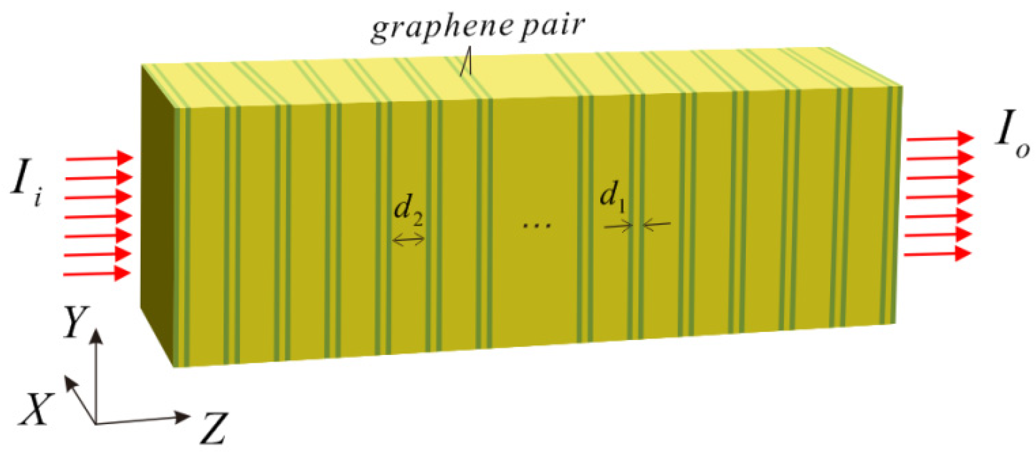
The graphene pairs are inserted in a bulk dielectric to form the graphene-pair arrays as shown in Figure 1. Here, the bulk dielectric is silicon dioxide (SiO2) with a refractive index of nd. Silicon dioxide is the substrate to install graphene pairs. The substrate material of silicon dioxide is homogeneous and presents isotropy in the THz band. The interval of the two graphene sheets in a graphene pair is denoted by d1 and here, is set as d1 = 10 nm. The spatial distance between two adjacent graphene pairs is d2 = 10 μm. The parameters satisfy the condition d2 ≫ d1. On the whole, the structure is periodic, and the spatial period of graphene pairs can be viewed as d = d1 + d2.
Graphene is an ultrathin two-dimensional nanomaterial and is generally treated as an equivalent dielectric with a considerable thickness of dg. This equivalent method for graphene is reasonable under the condition of dg < 1 nm, which has been verified by numerous experimental and simulating results [16,17].
The equivalent permittivity of graphene can be expressed as
Here, the equivalent thickness of graphene is set as dg = 0.33 nm. The symbol i is the imaginary unit. The parameter k0 represents the wave number of incident wave in vacuum and the vacuum resistivity parameter is denoted by η0. Other parameters are given as the following: the period number of graphene-pair arrays is N = 40 and the permittivity of SiO2 is provided with a fixed value of εd = (nd)2 = 2.1.
The conductivity of graphene is governed by the Kubo formula [19,20,21] and the complete expression is given by
where fd = 1/(1 + exp[(ξ − μ)/(kBTg)]) is the Fermi–Dirac distribution function, is the reduced Planck’s constant, kB is the Boltzmann’s constant, ξ is the electron energy, μ is the chemical potential of graphene, Tg is the environment temperature, −e is the charge of an electron, i is the imaginary unit, ω is the angular frequency, and τ is the phenomenological relaxation time of electrons. The environment temperature is set as Tg = 300 K. The integration for the first term of Equation (2) can be rewritten by
which dominates the scattering process of intraband electron–photon in graphene.
The excited motions of electrons in graphene not only include intraband transitions, but also the interband transitions. The second term of Equation (2) represents the interband scattering. For ℏω, |μ| ≫ kBTg, the interband scattering term can be simplified as
The interband and intraband transitions items both involve μ and ω, that is to say, the surface conductivity of graphene is a function of the chemical potential and the incident frequency of light. In THz wave band, the interband transitions are dominant, as the excited photon energy ℏω is lower than 2μ and the optical performance of graphene is similar to that of metals. In this case, the surface conductivity of graphene can be reduced to a Drude model.
The one-dimensional periodic photonic crystal based on graphene pairs arranges along the Z-axis. A light normally impinges on the structure from the left and transmits from the right. By ignoring the nonlinear effects of light, we give the linear transmission and reflection spectra of the periodic systems with the forward transmission matrix method (FTMM) [26].
The chemical potential of graphene is the Femi level, so the chemical potential can be controlled by chemical doping or an external gate voltage on graphene. As a positive value of voltage loads on graphene, the chemical potential of graphene increases, while the chemical potential of graphene decreases for a negative voltage biasing on graphene. Therefore, one can modulate the surface conductivity of graphene flexibly by a bias voltage on graphene.
3. Photonic Bandgaps
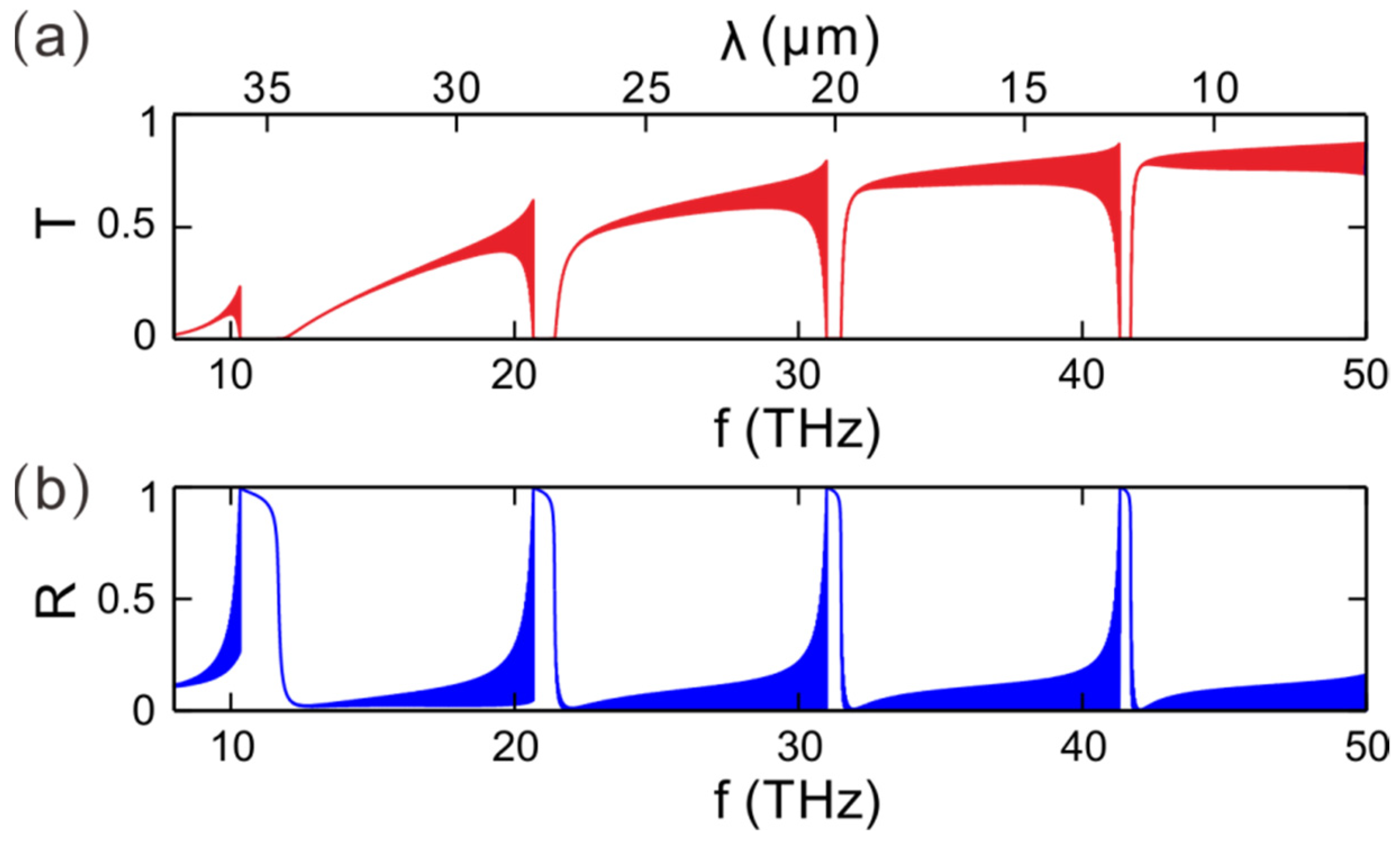
For a transverse magnetic (TM) wave, as it normally impinges on the periodic structures composed of graphene pairs from the left, Figure 2a gives the transmittance versus the frequency of light. The relaxation time is set as τ = 0.5 ps, and the graphene chemical potential is given by μ = 0.4 eV. The Bragg period number is N = 40. There are four photonic bandgaps in the spectrum in our given interval of frequency, and they are respectively defined as the first, the second, the third and the fourth bandgap in turn from left to right. The bandgap width declines as the frequency increases. The widths of the first ~ fourth bandgaps are 1.44, 0.74, 0.48 and 0.36 THz in order, and their corresponding center frequencies are 11.05, 21.04, 31.24 and 41.51 THz, respectively. On both sides of each bandgap, there are two passbands as well. Otherwise, the average transmittance of light in each transmission band can be elevated by increasing the incident frequency. The photonic bandgap is analogous to the energy band structure of electrons in semiconductors. The bandgaps in transmission spectra can naturally be utilized for band-stop filters [11], while the edge states at the bandgaps can greatly localize the electric field, which has extensively been applied to realize optical solitons [16,17], topological boundary states [27,28] and low threshold optical bistabilities [29,30,31]. The corresponding working wave of the filters is in the range of [6μm, 37.5μm], which locates at the middle-infrared band.
As the TM polarized light wave is incident on the graphene-pair arrays from the left, keeping the parameters above unchanged, the homologous reflection spectrum is provided in Figure 2b. There are four reflection pulses, viz. high reflectance sections, in the reflection curve as the frequency of light wave changes. The four frequency bands of high reflection exactly agree with the stopbands in the transmission spectrum, respectively. Otherwise, in the high reflection frequency bands, the reflectance is close to 1 at the rising edge of each reflection pulse and slightly lowers as the frequency increases. However, the value of reflection drops abruptly at the falling edge of each reflectance pulse.
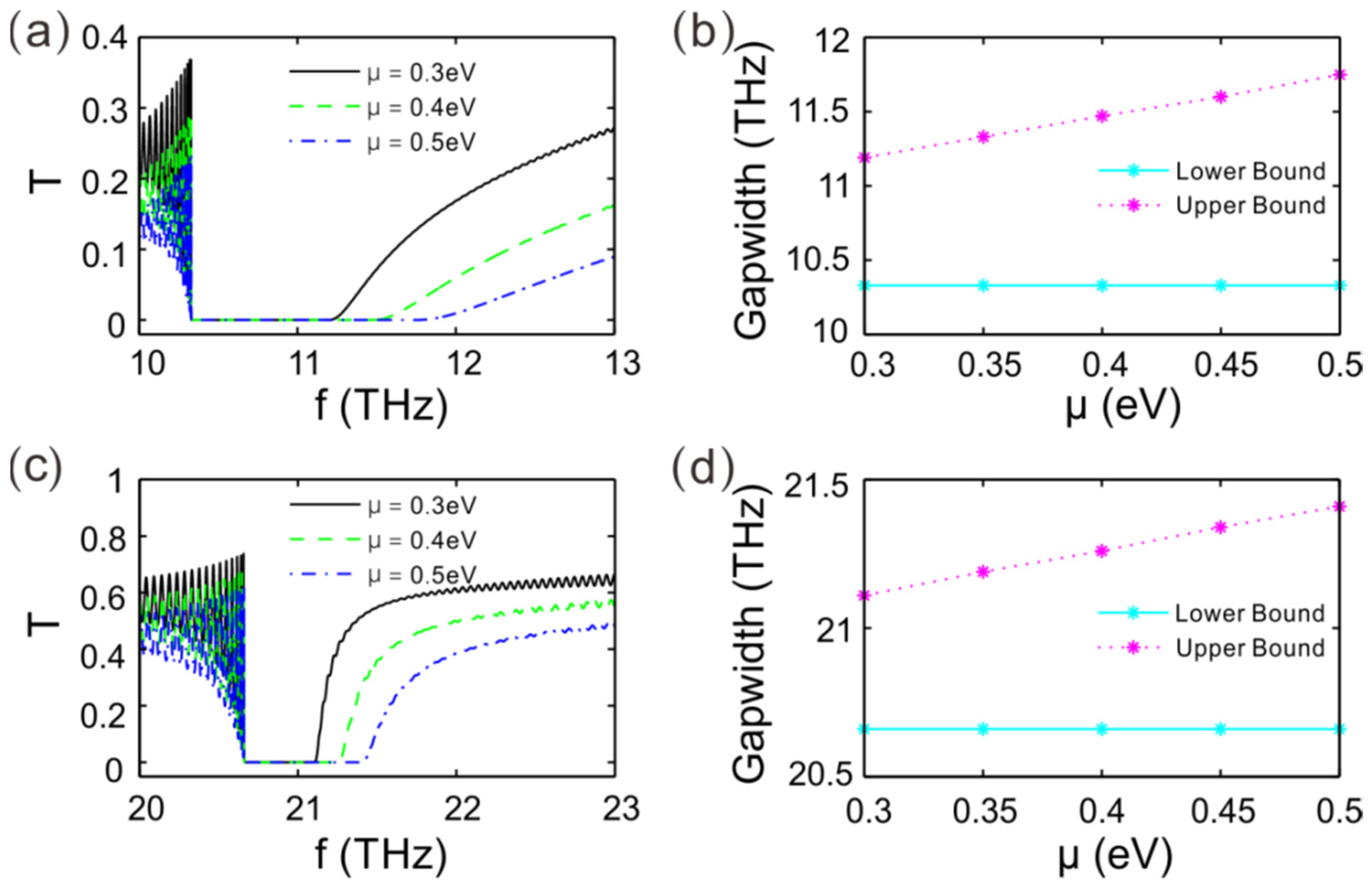
Since the chemical potential is one of the parameters which can affect the surface conductivity of graphene, the equivalent permittivity of graphene is a function of the chemical potential μ. Subsequently, one can modulate the transmission performance of the periodic structure by the graphene chemical potential flexibly. For different values of chemical potential, Figure 3a provides the transmittance varying with the frequency of light wave around the first stopband. As a TM-polarized light is normally left incident on the arrays, the falling edge position of the first band always stays unchanged as the chemical potential increases. The transmittance is equal to zero at the first bandgap, which means that there is no light that can transmit this periodic structure as an incident light wavelength locates at the stopband. By increasing the frequency of light, there is an inflection point at the right of each transmission stopband, and then the transmittance increases as the frequency passes the inflection point. We define the interval between the falling edge and the inflection point as the stopband width.
The inflection point at each stopband is moving to the right by modulating the chemical potential to a larger value. In other words, the bandgap width enlarges as the chemical potential increases. On the right of each bandgap, the transmittance is not zero and it increases with the increase in light frequency. Meanwhile, for a non-zero transmittance at the right rising edge of stopband, the transmittance decreases with the increase in the chemical potential for a fixed incident wavelength.
Figure 3b gives the relationship between the stopband width of light and the chemical potential of graphene. The gap width is equal to the deviation between the upper and lower boundaries of stopband. One can see that the lower boundary of bandgap is unchanged as the graphene chemical potential increases, while the upper boundary increases with the increase in the chemical potential. Hence, the gap width can be modulated by changing the value of the graphene chemical potential.
Compared with the first stopband, the gap width of the second stopband is narrower for the same value of graphene chemical potential as shown in Figure 3c. Similarly, the right transmittance from the graphene-pair arrays is zero for the light wave that locates in the bandgap, which forms a stopband of light waves. On both sides of the stopband, the transmittance is relatively lower for a larger value of chemical potential. The left boundary (trailing edge) of the bandgap stays the same position for different values of the chemical potential, while on the right boundary (rising edge) of the bandgap, the curve gets steeper for a lower value in chemical potential. Otherwise, in comparison with the first bandgap, the extinction ratio at the rising edge of the second bandgap is better.
Similar to the first bandgap, the inflection point on the right boundary of the second bandgap moves rightwards as the chemical potential increases. Specifically, the width of the second bandgap is proportional to the chemical potential as shown in Figure 3d. Therefore, one can modulate the second stopband gap width by changing the chemical potential, but the starting position of the second bandgap always remains unchanged.
Figure 4a gives the real part of graphene surface conductivity Re(σ) for different values of chemical potential. For three given values of μ = 0.3, 0.4 and 0.5 eV, there are three curves, correspondingly, of Re(σ) as the light frequency changes. The real part of graphene surface conductivity decreases with the frequency of light increasing for a fixed value of graphene chemical potential. On the other hand, a larger value of Re(σ) can be obtained by tuning the chemical potential up to a bigger value, as the incident wavelength is determined. The parameter Re(σ) is the counterpart of the imaginary part of the graphene equivalent dielectric constant Im(εg), which represents the optical loss in graphene. Therefore, for a larger Re(σ) of graphene, it means that the corresponding optical loss is greater in systems. With the increase in light frequency, the loss gradually decreases as well. This approves the phenomenon of each passband transmittance in sequence increasing with the frequency of incident light as shown in Figure 2a.
Figure 4b demonstrates Re(σ) variation in the parameter space composed of the chemical potential and light frequency. One can see that, except for the corner of the parameter space on the left, the value of Re(σ) increases by raising the graphene chemical potential or turning down the light frequency. Since Re(σ) governs the loss in graphene of light, changing the graphene chemical potential or modulating the light frequency are important measures in manipulating light propagation in the graphene-pair arrays. Around the parameters of μ = 0.2 eV and f = 100 THz, there is an abrupt change in Re(σ). It results from the transformation of electrons intraband transition to interband transition in graphene.
Figure 4c gives the imaginary part of surface conductivity Im(σ) changing with the light frequency. For different values of μ = 0.3, 0.4 and 0.5 eV, it shows that Im(σ) decreases with the increase in light frequency in each of the three corresponding curves. Similarly, for a given incident wavelength, a larger chemical potential induces a bigger value in Im(σ). The imaginary part of surface conductivity determines the real part of εg. Moreover, Im(σ) is a function of the chemical potential μ. Therefore, we can modulate the stopband width by changing the structure parameter through an external gate voltage on graphene as shown in Figure 3c.
Figure 4d describes Im(σ) changing with the chemical potential and light frequency in the parameter space. It shows that Im(σ) increases with the raise of the graphene chemical potential and decrease in the light frequency. The parameter of Im(σ) determines the real part of graphene equivalent permittivity and Im(σ) can be changed by μ, so we can regulate the transmittance by the graphene chemical potential flexibly.
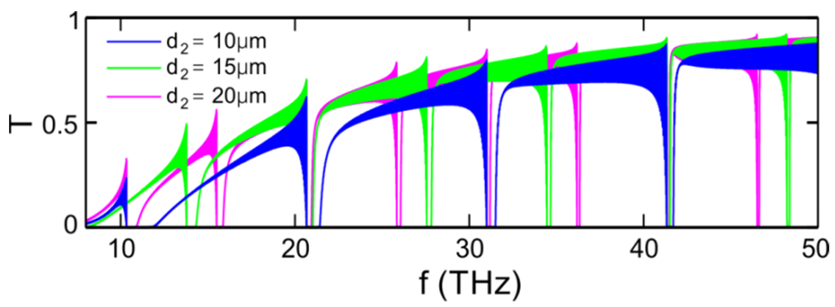
The interval between two adjacent graphene pairs is d2 and the spatial period of graphene-pair arrays is d1 + d2. The parameter d2 can also affect the transmission spectrum of light and the stopband width and the position in the transmission spectrum. For different values of d2, Figure 5 gives the transmittance by changing the frequency of the light wave. As a light impinges on the arrays from the left, it demonstrates that there are four stopbands in the frequency range of [10, 50] THz as the spatial distance is d2 = 10 μm, and the stopband number respectively increases to 6 and 8 for d2 = 15 and 20 μm. Therefore, one can regulate the stopband number by tuning the value of d2.
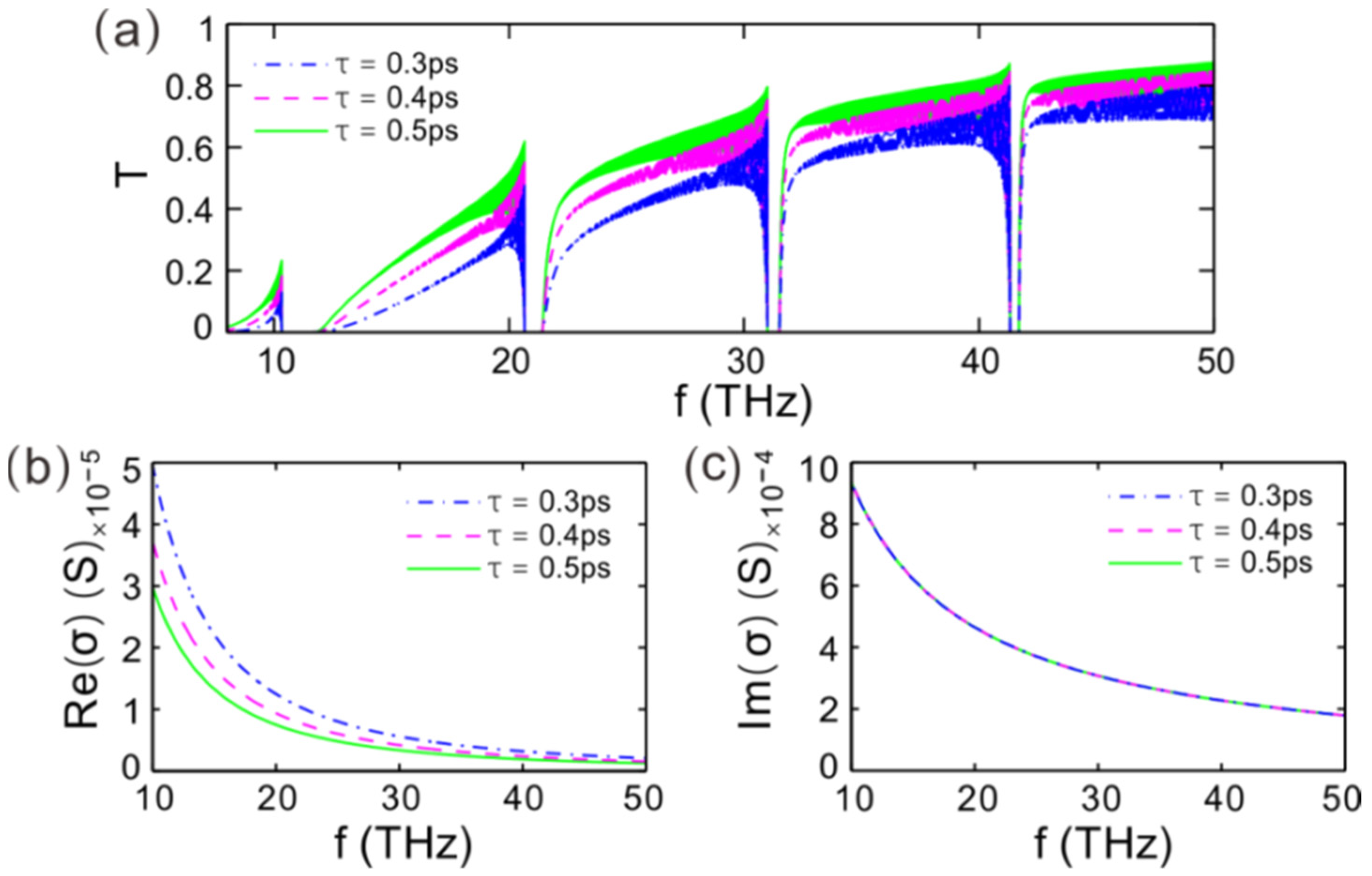
As mentioned in Equation (2), the surface conductivity of graphene is a function of the parameter of τ, which is defined as the phenomenological relaxation time of electrons in graphene. Figure 6a gives the transmission spectra for different values of τ. One can see that all of the bandgap positions in the spectra hold still as the parameter τ varies arbitrarily. However, on the whole, the photonic passbands in the transmission spectra are elevated with the value increases in τ. That is because the optical loss in graphene reduces as the phenomenological relaxation time rises. The phenomenological relaxation time only governs the surface conductivity of graphene but does not determine the geometric parameters of the structure composed of graphene-pair arrays. Therefore, the stopband gap positions in the transmission spectra are unaffected by τ.
The graphene surface conductivity σ is also a function of the phenomenological relaxation time τ. Figure 6b gives the real surface conductivity Re(σ) for different values of τ. For three given values of τ = 0.3, 0.4 and 0.5 ps, the value of Re(σ) in each corresponding curve changes with the light frequency. As mentioned above, the real part Re(σ) decides the optical loss in graphene. Since Re(σ) decreases with the increase in the light frequency for a given value of τ, the transmittance increases by turning up the frequency of light as shown in Figure 6a. Otherwise, it also shows that, by fixing the incident frequency, a lower value of τ corresponds to a bigger Re(σ), which means that a larger optical loss may be induced.
However, the imaginary part of surface conductivity Im(σ) is not affected by τ as shown in Figure 6c. The value of Im(σ) decreases with the increase in the light frequency for different values of τ, but the three surface conductivity curves almost coincide with each other for τ = 0.3, 0.4 and 0.5 ps. The parameter of Im(σ) governs the real equivalent permittivity of graphene, so one cannot affect the stopbands in the transmission spectrum by modulating the phenomenological relaxation time.
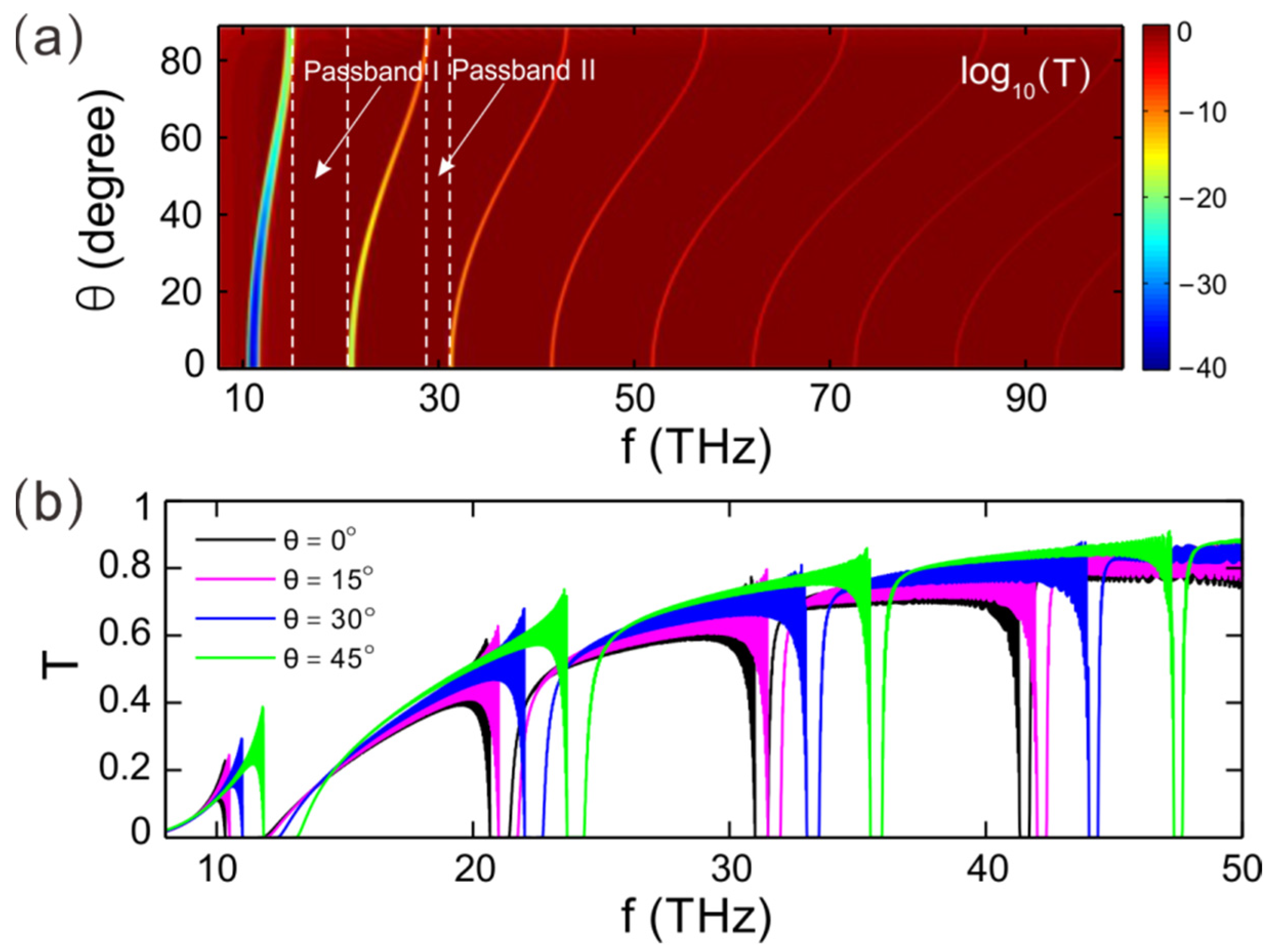
Figure 7a demonstrates the transmittance in the parameter space. The parameter space is composed of the incident angle and the light frequency. For the left incident light, the fringes of brighter color in transmission space represent the photonic bandgaps of light, i.e., the stopbands. For a sharp contrast, we have taken the logarithm of transmittance. The gap widths of these fringes decrease from the left to the right as the light frequency increases. For each stopband, the fringe profile in transmission moves toward higher frequency by promoting the incident angle. There is a full transmission band between the first stopband and the second stopband. We have denoted the full passband by passband I, which is sandwiched by two dotted lines. It means that, no mater how the incident angle changes, the incident light waves can transmit this structure as a light frequency locates in passband I. Furthermore, there is also another full transmission band labeled by passband II. Passband II is local between the second stopband and the third stopband. The width of passband II is narrower than that of passband I. There are two passbands in the transmission parameter space and as the frequency increases, there is no new full transmission band that arises.
For four given incident angles, Figure 7b provides the corresponding transmission spectra of light wave. It shows that the spectrum profile moves rightwards on the whole by increasing the incident angle. The bandgaps widths of the same ordinal stay unchanged. Therefore, the stopband position of light frequency in the transmission spectrum can be modulated by changing the incident angle as well. For a fixed wavelength, the Z-axis component of the corresponding wave vector is minished by turning up the incident angle, so the bandgap position moves towards a shorter wavelength.
The system is a one-dimensional periodic structure along the Z-axis, and the XY-plane is infinite. In experiments, as long as the sizes of the device in the X and Y directions are two orders of magnitude larger than the incident wavelength, the design conditions can be satisfied. Large areas and high-quality monolayers of graphene and dielectric layers can be stacked layer by layer by chemical vapor deposition [32,33]. This is a common and well-established technique that has been widely used in the manufacture of integrated circuits. Otherwise, graphene arrays have been utilized for the electron acceptors experimentally as well [34,35]. Therefore, it would be desirable to realize the stopband filters based on graphene-pair arrays in laboratory. As a light beam composed of plenty of wavelengths impinges on the periodic structure, the light waves locating at the stopband may be reflected by the system and the other wavelengths of light can be transmitted.
Considering the loss in the substrate dielectric SiO2 in THz band, the refractive index of material can be denoted by nd = ndr + indi, where ndr and ndi are the real and imaginary parts, respectively. The symbol of ndi is also called the extinction coefficient, representing the optical loss of materials. In the THz band, the optical loss in SiO2 is considerable and there are two peaks around 3.96 THz and 7.94 THz in the absorption spectrum [36]. Furthermore, the value of the extinction coefficient decreases with the increases in the temperature. In our concerned wave band, the average value of the extinction coefficient of SiO2 here is approximately equal to ndi ≈ 0.001. Compared with the lossless case of ndi = 0, the transmittance in the passbands and the reflectance in the stopband both decrease. Otherwise, with the increase in the light wave, the transmission and reflection of light beam decrease as well. However, the bandgap number and each position of the bandgaps are unchanged in the spectra for ndi = 0 and 0.001. Therefore, the loss on substrate may affect the transmission and reflection in the passbands or stopbands, but it is not the physical mechanism in the formation of stopbands, which are induced by the periodic graphene-pair arrays. Of course, we can also choose a material with a uniform refractive index and low loss coefficient as the substrate.
4. Conclusions
In conclusion, multiple photonic bandgaps and their regulations were investigated in a complex system composed of a bulk dielectric and graphene pairs. Graphene pairs arrange in the substrate material to form periodic graphene arrays. Series of bandgaps are induced in transmission spectra and the central bandgap frequencies and widths can be tuned by the graphene chemical potential. The interval between to adjacent bandgaps is inversely proportional to the spatial period of the graphene pair. The transmittance of passbands between the bandgaps is a function of the phenomenological relaxation time as well. Furthermore, by scanning the incident angle and light frequency, two full passbands can be achieved around the first and second bandgaps. The study could provide a feasible scheme for photonic stopband filters.
Author Contributions
Software, D.Z. (Dong Zhao) and L.W.; formal analysis, D.Z. (Dong Zhao) and M.W.; investigation, L.W. and F.L.; resources, L.W.; data curation, M.W.; writing—original draft preparation, D.Z. (Dong Zhao); writing—review and editing, F.L., D.Z. (Dong Zhong) and M.W.; visualization, L.W.; supervision, D.Z. (Dong Zhong) and M.W.; project administration, M.W.; funding acquisition, D.Z. (Dong Zhao), L.W., F.L., D.Z. (Dong Zhong) and M.W. All authors have read and agreed to the published version of the manuscript.
Funding
National Natural Science Foundation of China (NSFC) (51975542); the Scientific Research Project of Hubei University of Science and Technology (BK202017, 2021-23GP01, 2022-23X11, 2021-22X21); the Science and Technology Plan Research Project of Hubei Education Department (B2020155).
Institutional Review Board Statement
Not applicable.
Informed Consent Statement
Not applicable.
Data Availability Statement
Not applicable.
Conflicts of Interest
The authors declare no conflict of interest.
References
- Fathpour, S.; Abdelsalam, K.; Ordouie, E.; Vazimali, M.G.; Kumar, P. Tunable dual-channel ultra-narrowband Bragg grating filter on thin-film lithium niobate. Opt. Lett. 2021, 46, 2730–2733. [Google Scholar]
- Feng, X.; Liu, Y.; Yuan, S.; Kai, G.; Zhang, W.; Dong, X. L-Band switchable dual-wavelength erbium-doped fiber laser based on a multimode fiber Bragg grating. Opt. Express 2004, 12, 3834–3839. [Google Scholar] [CrossRef] [PubMed]
- Wang, F.; Liu, Y.; Bi, W. Tunable erbium-doped-fiber laser based on the double-superimposed fiber Bragg gratings. Optik 2021, 246, 167777. [Google Scholar]
- Wu, Y.; Shi, Y.; Zhao, Y.; Li, L.; Chen, X. On-chip optical narrowband reflector based on anti-symmetric Bragg grating. Opt. Express 2019, 27, 38541–38552. [Google Scholar] [CrossRef] [PubMed]
- Xie, W.; Li, J.; Liao, M.; Deng, Z.; Wang, W.; Sun, S. Narrow linewidth distributed Bragg reflectors based on InGaN/GaN laser. Micromachines 2019, 10, 529. [Google Scholar] [CrossRef] [Green Version]
- Chaudhry, M.R.; Zakwan, M.; Onbasli, M.C.; Serpengüzel, A. Symmetric meandering distributed feedback structures for silicon photonic circuits. IEEE J. Sel. Top. Quantum Electron. 2019, 26, 6100505. [Google Scholar] [CrossRef]
- Dobb, H.; Webb, D.J.; Kalli, K.; Argyros, A.; Large, M.C.J.; Eijkelenborg, M.A.V. Continuous wave ultraviolet light-induced fiber Bragg gratings in few- and single-mode microstructured polymer optical fibers. Opt. Lett. 2005, 30, 3296–3298. [Google Scholar]
- Mills, J.D.; Hillman, C.; Blott, B.H.; Brocklesby, W.S. Imaging of free-space interference patterns used to manufacture fiber Bragg gratings. Appl. Opt. 2000, 39, 6128–6135. [Google Scholar] [CrossRef] [PubMed]
- Wan, B.F.; Wang, P.X.; Xu, Y.; Zhang, D.; Zhang, H.F. A space filter possessing polarization separation characteristics realized by 1-D magnetized plasma photonic crystals. IEEE Trans. Plasma Sci. 2021, 49, 703–710. [Google Scholar] [CrossRef]
- Park, S.; Norton, B.; Boreman, G.D.; Hofmann, T. Mechanical tuning of the terahertz photonic bandgap of 3d-printed one-dimensional photonic crystals. J. Infrared Millim. Terahertz Waves 2021, 42, 220–228. [Google Scholar] [CrossRef]
- Trabelsi, Y.; Ali, N.B.; Kanzari, M. Tunable narrowband optical filters using superconductor/dielectric generalized Thue-Morse photonic crystals. Microelectron. Eng. 2019, 213, 41–46. [Google Scholar] [CrossRef]
- Liu, Q.; Liu, J.; Zhao, D.; Wang, B. On-chip experiment for chiral mode transfer without enclosing an exceptional point. Phys. Rev. A 2021, 103, 023531. [Google Scholar] [CrossRef]
- Geim, A.K.; Novoselov, K.S. The rise of graphene. Nat. Mater. 2007, 6, 183–191. [Google Scholar] [CrossRef] [PubMed]
- Berman, O.L.; Kezerashvili, R.Y. Graphene-based one-dimensional photonic crystal. J. Phys. Condens. Matter 2011, 24, 015305. [Google Scholar] [CrossRef]
- Wang, Z.; Bing, W.; Hua, L.; Kai, W.; Lu, P. Plasmonic lattice solitons in nonlinear graphene sheet arrays. Opt. Express 2015, 23, 32679–32689. [Google Scholar] [CrossRef] [PubMed]
- Wang, Z.; Wang, B.; Long, H.; Wang, K.; Lu, P. Surface plasmonic lattice solitons in semi-infinite graphene sheet arrays. J. Lightwave Technol. 2017, 34, 2960. [Google Scholar] [CrossRef] [Green Version]
- Wang, Z.; Wang, B.; Wang, K.; Long, H.; Lu, P. Vector plasmonic lattice solitons in nonlinear graphene-pair arrays. Opt. Lett. 2016, 41, 3619. [Google Scholar] [CrossRef] [Green Version]
- Feng, W.; Wang, Z.; Qin, C.; Bing, W.; Lu, P. Asymmetric plasmonic supermodes in nonlinear graphene multilayers. Opt. Express 2017, 25, 1234. [Google Scholar]
- Zhao, X.; Xu, B.; Kong, X.; Zhong, D.; Zhao, D. Tunable optical bistability, tristability and multistability in arrays of graphene. Appl. Sci. 2020, 10, 5766. [Google Scholar] [CrossRef]
- Feng, W.; Qin, C.; Bing, W.; Hua, L.; Lu, P. Rabi oscillations of plasmonic supermodes in graphene multilayer arrays. IEEE J. Sel. Top. Quantum Electron. 2016, 23, 4600165. [Google Scholar]
- Wang, F.; Qin, C.; Wang, B.; Ke, S.; Long, H.; Wang, K.; Lu, P. Rabi oscillations of surface plasmon polaritons in graphene-pair arrays. Opt. Express 2015, 23, 31136–31143. [Google Scholar] [CrossRef] [PubMed]
- Ioannidis, T.; Gric, T.; Rafailov, E. Surface plasmon polariton waves propagation at the boundary of graphene based metamaterial and corrugated metal in THz range. Opt. Quantum Electron. 2020, 52, 10. [Google Scholar] [CrossRef]
- Ioannidis, T.; Gric, T.; Rafailov, E. Tunable polaritons of spiral nanowire metamaterials. Waves Random Complex 2020. [Google Scholar] [CrossRef]
- Ma, T.; Yuan, J.; Wang, F.; Liu, H.; Liu, Y. Graphene-coated two-layer dielectric loaded surface plasmon polariton rib waveguide with ultra-long propagation length and ultra-high electro-optic wavelength tuning. IEEE Access 2020, 8, 103433–103442. [Google Scholar] [CrossRef]
- Hajian, H.; Soltani-Vala, A.; Kalafi, M. Tunable far-IR bandgaps in a one-dimensional graphene-dielectric photonic crystal. Phys. Status Solidi 2012, 9, 2614–2617. [Google Scholar] [CrossRef]
- Fang, Y.T.; Liang, Z.C. Unusual transmission through usual one-dimensional photonic crystal in the presence of evanescent wave. Opt. Commun. 2010, 283, 2102–2108. [Google Scholar] [CrossRef]
- Lin, Z.; Ke, S.; Zhu, X.; Li, X. Square-root non-Bloch topological insulators in non-Hermitian ring resonators. Opt. Express 2021, 29, 419852. [Google Scholar] [CrossRef]
- Malkova, N.; Hromada, I.; Wang, X.; Bryant, G.; Chen, Z. Observation of optical Shockley-like surface states in photonic superlattices. Opt. Lett. 2009, 34, 1633–1635. [Google Scholar] [CrossRef] [PubMed]
- Wang, J.; Xu, F.; Liu, F.; Zhao, D. Optical bistable and multistable phenomena in aperiodic multilayer structures with graphene. Opt. Mater. 2021, 119, 111395. [Google Scholar] [CrossRef]
- Ni, H.; Wang, J.; Wu, A. Optical bistability in aperiodic multilayer composed of graphene and Thue-Morse lattices. Optik 2021, 242, 167163. [Google Scholar] [CrossRef]
- Wu, Y.; Zhao, X.; Hu, J.; Xu, H. Low threshold optical bistability based on coupled graphene Tamm states. Results Phys. 2021, 21, 103824. [Google Scholar] [CrossRef]
- Guo, C.X.; Yang, H.B.; Sheng, Z.M.; Lu, Z.S.; Song, Q.L.; Li, C.M. Layered graphene/quantum dots for photovoltaic devices. Angew. Chem. Int. Edit. 2010, 49, 3014–3017. [Google Scholar] [CrossRef] [PubMed]
- Wang, Y.; Chen, X.; Zhong, Y.; Zhu, F.; Loh, K.P. Large area, continuous, few-layered graphene as anodes in organic photovoltaic devices. Appl. Phys. Lett. 2009, 95, 209. [Google Scholar] [CrossRef]
- Wang, S.; Goh, B.M.; Manga, K.K.; Bao, Q.; Yang, P.; Loh, K.P. Graphene as atomic template and structural scaffold in the synthesis of graphene−organic hybrid wire with photovoltaic properties. ACS Nano 2010, 4, 6180–6186. [Google Scholar] [CrossRef] [PubMed]
- Xu, G.; Abbott, J.; Qin, L.; Yeung, K.; Song, Y.; Yoon, H.; Kong, J.; Ham, D. Electrophoretic and field-effect graphene for all-electrical dna array technology. Nat. Commun. 2014, 5, 4866. [Google Scholar] [CrossRef] [Green Version]
- Davies, C.L.; Patel, J.B.; Xia, C.Q.; Herz, L.M.; Johnston, M.B. Temperature-dependent refractive index of quartz at terahertz frequencies. J. Infrared Millim. Terahertz Waves 2018, 39, 1236–1248. [Google Scholar] [CrossRef] [Green Version]
Figure 1.
Schematic of graphene-pair arrays. The synthesized arrays are constructed by graphene sheets and dielectrics. The spatial period of graphene pairs is given by d = d1 + d2.
Figure 1.
Schematic of graphene-pair arrays. The synthesized arrays are constructed by graphene sheets and dielectrics. The spatial period of graphene pairs is given by d = d1 + d2.

Figure 2.
(a,b) Transmission and reflection spectra for the normally incident light waves from the left, respectively. The spatial intervals are set as d1 = 10 nm and d2 = 10 μm, respectively.
Figure 2.
(a,b) Transmission and reflection spectra for the normally incident light waves from the left, respectively. The spatial intervals are set as d1 = 10 nm and d2 = 10 μm, respectively.

Figure 3.
(a) Transmittance around the first bandgap for different values of graphene chemical potential. (b) The first stopband gapwidth varying with the chemical potential. (c) Transmittance around the second bandgap for different values of chemical potential. (d) Gapwidth of the second stopband varying with the chemical potential.

Figure 4.
(a,c) Real part and imaginary part of graphene surface conductivity varying with the light frequency for different values of chemical potential, respectively. (b,d) Real part and imaginary part of graphene surface conductivity by modulating simultaneously the light frequency and chemical potential, respectively.

Figure 5.
Transmittance varying with the frequency of light wave for different spatial intervals of two adjacent graphene pairs. The graphene chemical potential is μ = 0.4 eV, and the relaxation time is set as τ = 0.5 ps.
Figure 5.
Transmittance varying with the frequency of light wave for different spatial intervals of two adjacent graphene pairs. The graphene chemical potential is μ = 0.4 eV, and the relaxation time is set as τ = 0.5 ps.

Figure 6.
(a) Dependence of the transmission spectra on the phenomenological relaxation time τ. (b,c) Real part and imaginary part of graphene surface conductivity varying with τ, respectively. The graphene chemical potential is set as μ = 0.4 eV for (a–c).
Figure 6.
(a) Dependence of the transmission spectra on the phenomenological relaxation time τ. (b,c) Real part and imaginary part of graphene surface conductivity varying with τ, respectively. The graphene chemical potential is set as μ = 0.4 eV for (a–c).

Figure 7.
(a) Transmittance in the parameter space composed of the incident angle and the light frequency. (b) Transmission spectra for different fixed incident angles. The spatial distance is d2 = 10 μm, the graphene chemical potential is μ = 0.4 eV, and the relaxation time is set as τ = 0.5 ps.
Figure 7.
(a) Transmittance in the parameter space composed of the incident angle and the light frequency. (b) Transmission spectra for different fixed incident angles. The spatial distance is d2 = 10 μm, the graphene chemical potential is μ = 0.4 eV, and the relaxation time is set as τ = 0.5 ps.


Table 1.
Research progress on graphene arrays.
| Structures | Authors | Optical Effects | Refs. |
|---|---|---|---|
| Graphene arrays | Wang, Z. et al. | Spatial solitons | [15] |
| Graphene arrays | Zhao, X. et al. | Optical bistability | [19] |
| Graphene multilayers | Wang, F. et al. | Plasmonic supermodes | [18] |
| Graphene multilayers | Wang, F. et al. | Rabi oscillations | [20] |
| Semi-infinite graphene arrays | Wang, Z. et al. | Surface solitons | [16] |
| Graphene-pair arrays | Wang, F. et al. | Rabi oscillations | [21] |
| Graphene-pair arrays | Wang, Z. et al. | Vector solitons | [17] |
Publisher’s Note: MDPI stays neutral with regard to jurisdictional claims in published maps and institutional affiliations. |
© 2021 by the authors. Licensee MDPI, Basel, Switzerland. This article is an open access article distributed under the terms and conditions of the Creative Commons Attribution (CC BY) license (https://creativecommons.org/licenses/by/4.0/).
Share and Cite
MDPI and ACS Style
Zhao, D.; Wang, L.; Liu, F.; Zhong, D.; Wu, M. Photonic Stopband Filters Based on Graphene-Pair Arrays. Appl. Sci. 2021, 11, 11557. https://0-doi-org.brum.beds.ac.uk/10.3390/app112311557
AMA Style
Zhao D, Wang L, Liu F, Zhong D, Wu M. Photonic Stopband Filters Based on Graphene-Pair Arrays. Applied Sciences. 2021; 11(23):11557. https://0-doi-org.brum.beds.ac.uk/10.3390/app112311557
Chicago/Turabian StyleZhao, Dong, Liyan Wang, Fangmei Liu, Dong Zhong, and Min Wu. 2021. "Photonic Stopband Filters Based on Graphene-Pair Arrays" Applied Sciences 11, no. 23: 11557. https://0-doi-org.brum.beds.ac.uk/10.3390/app112311557
Note that from the first issue of 2016, this journal uses article numbers instead of page numbers. See further details here.