
Towards Monolithic Indium Phosphide (InP)-Based Electronic Photonic Technologies for beyond 5G Communication Systems

 , , , , , ,
  and
and
Abstract
:1. Introduction
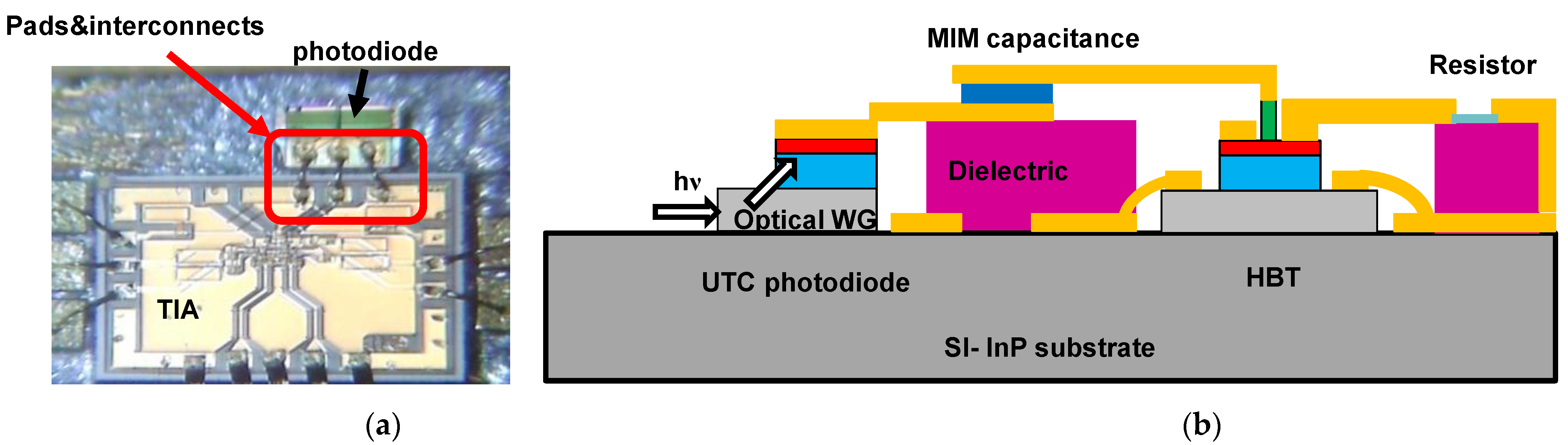
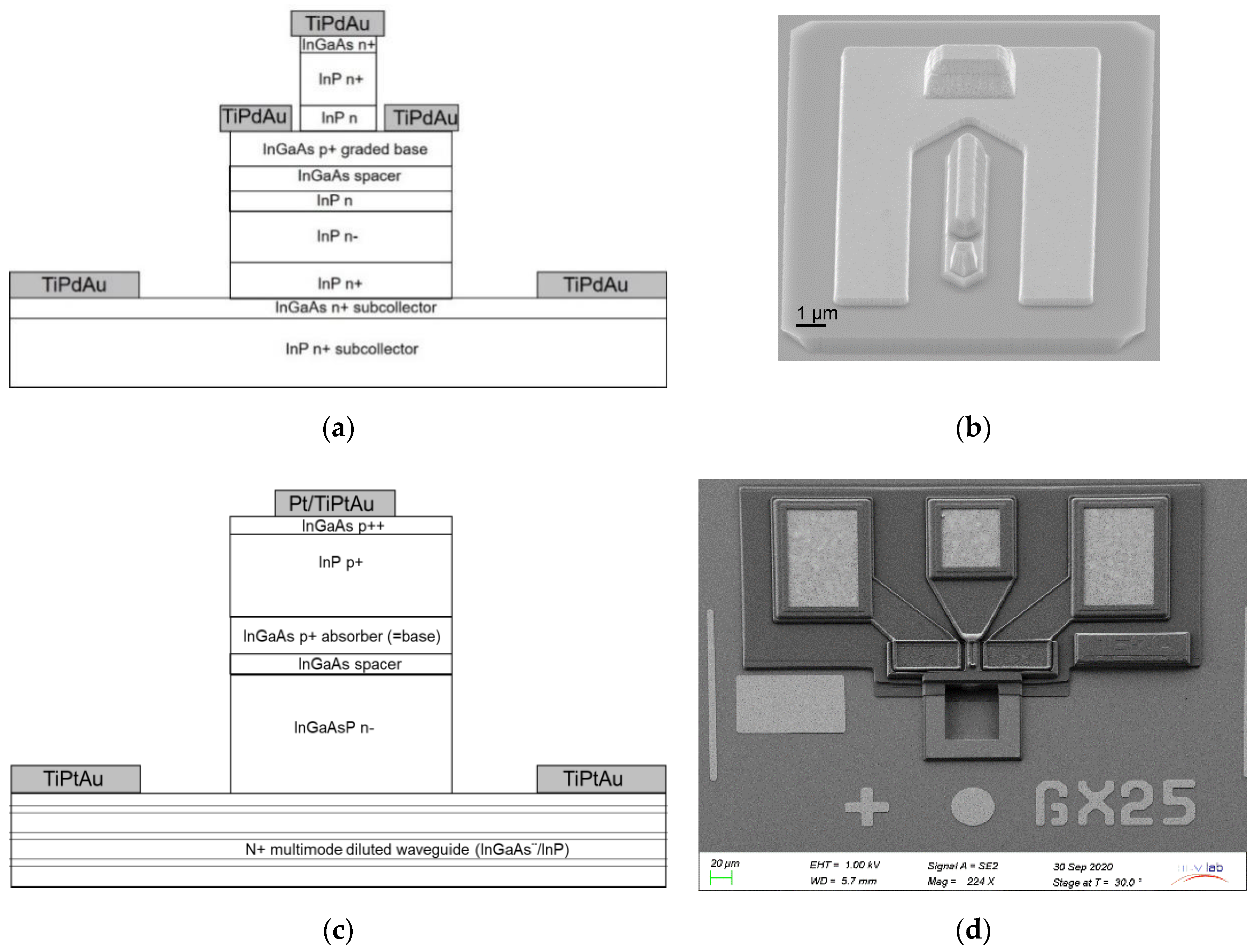
2. Technologies
3. Compact Modelling
3.1. DHBT Compact Modeling
3.2. UTC Photodiode Compact Modeling
3.2.1. Dark Current
3.2.2. Photocurrent
4. DC Characterization and Model Validation
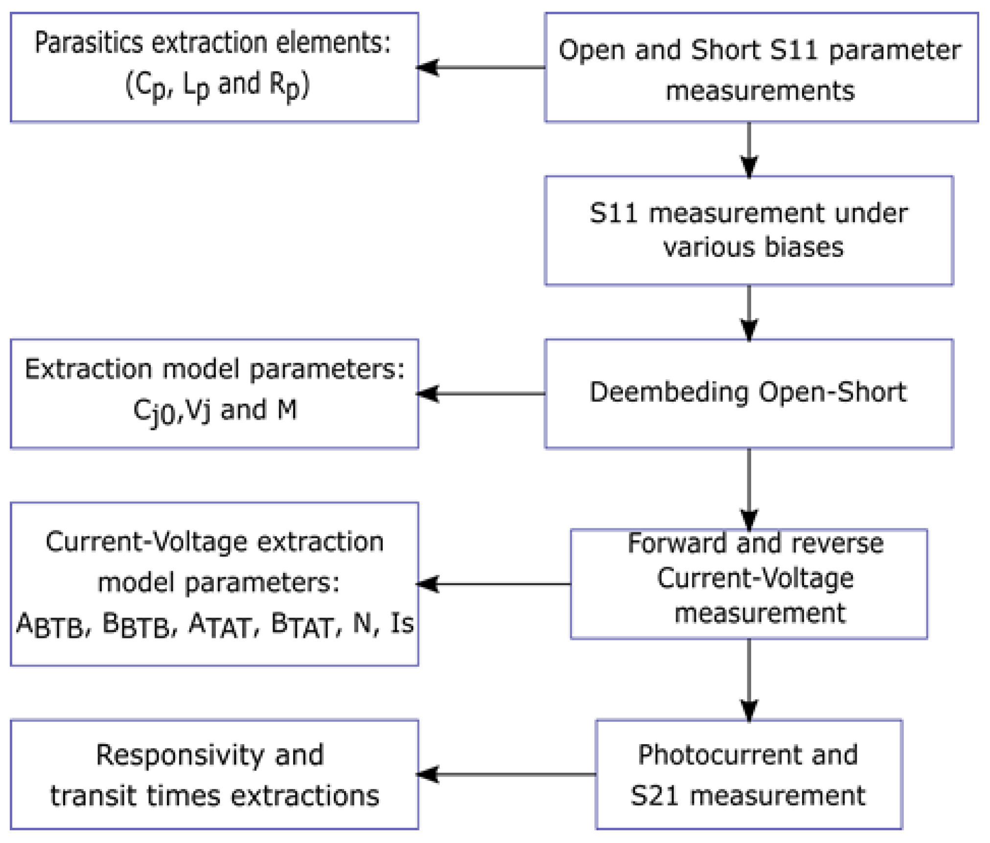
4.1. HiCuM Parameter Extraction Methodology
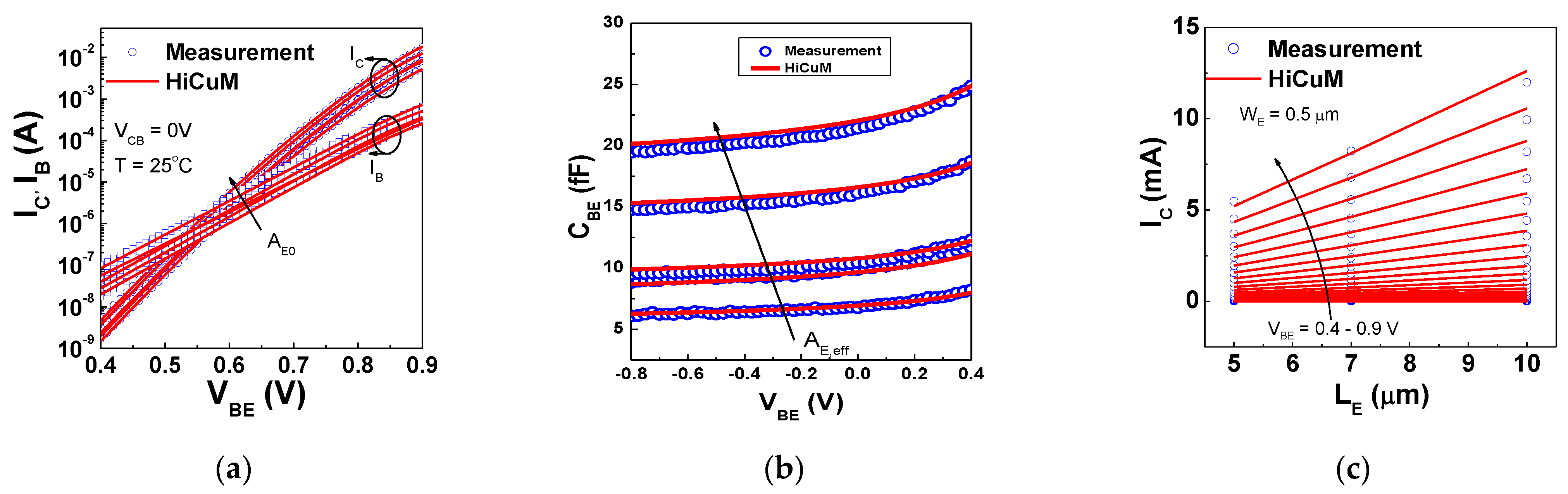
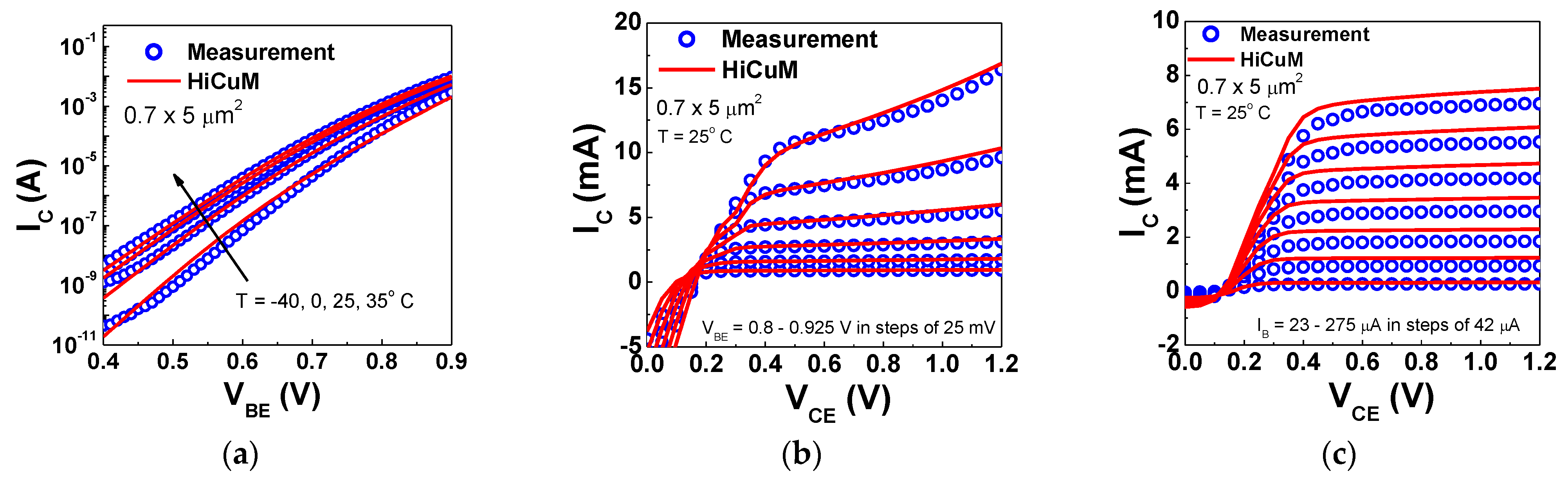
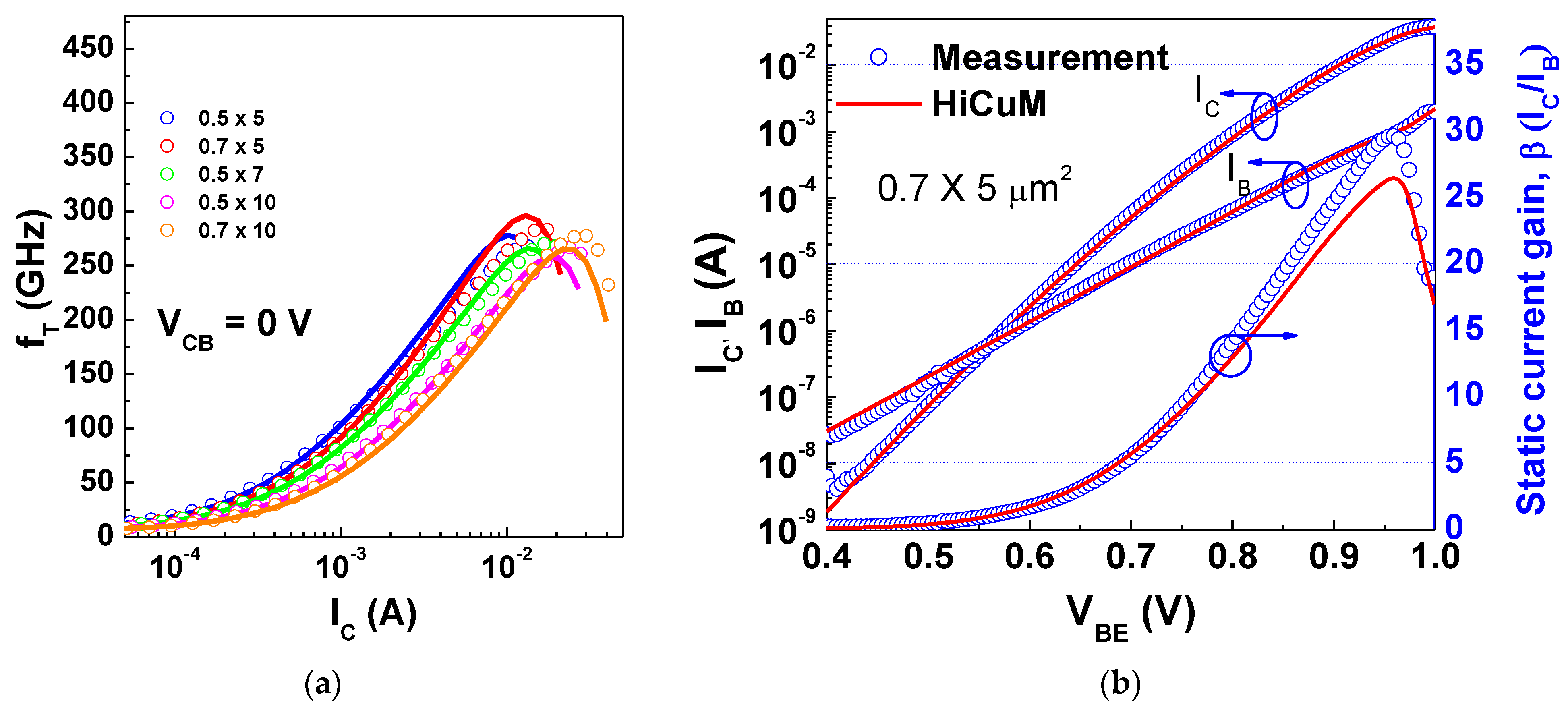
4.2. Geometry Scalable HiCuM Model Simulation of InP DHBTs
4.3. UTC Photodiode Compact Model Validation
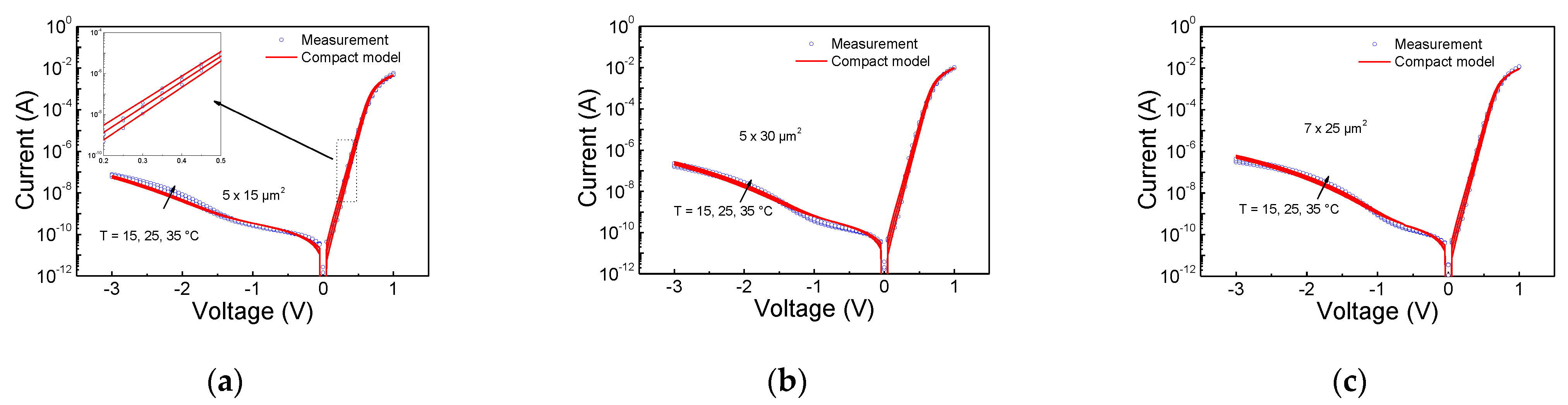
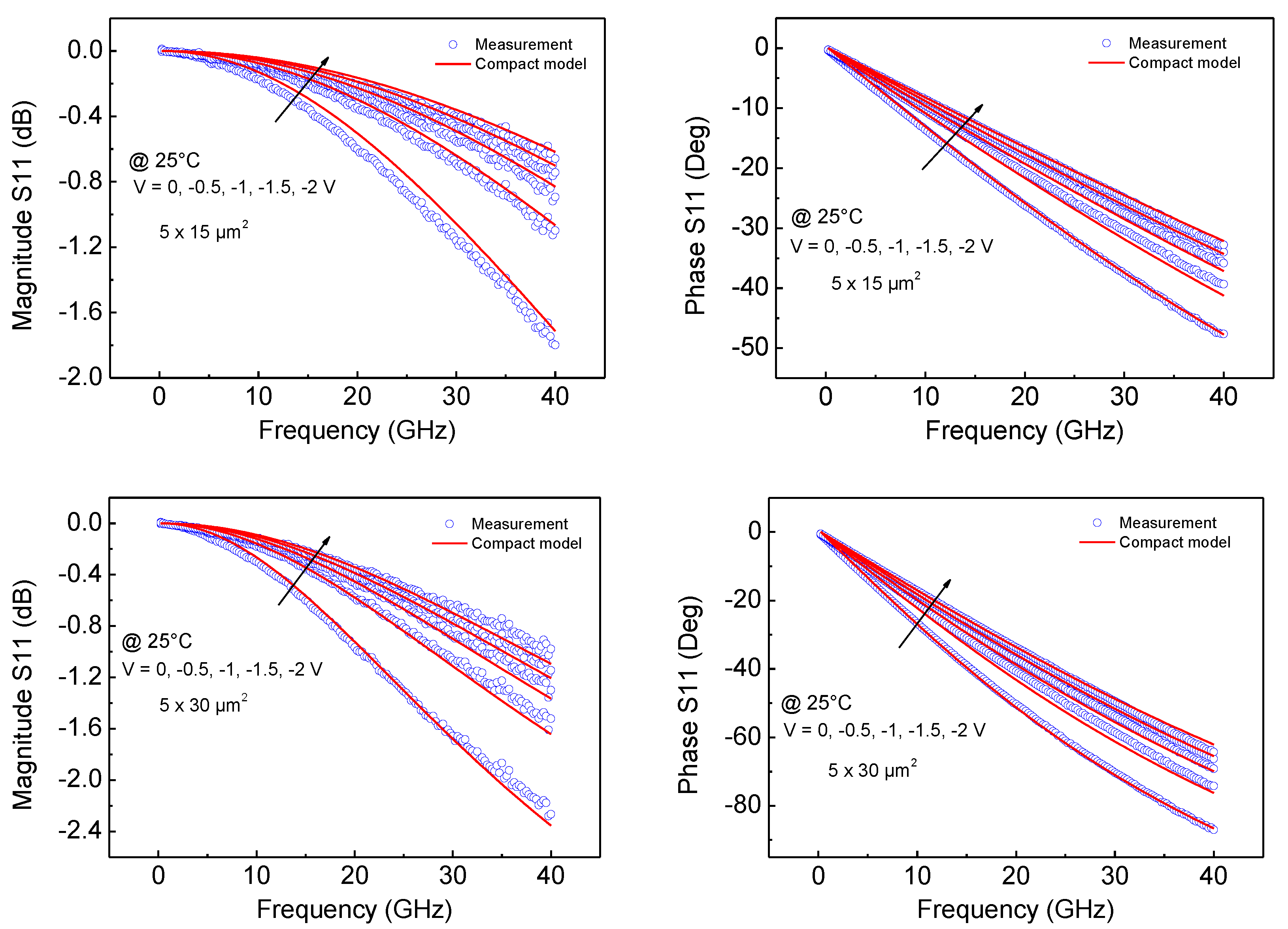
4.3.1. I–V Characterization and Parameter Extraction
4.3.2. Photocurrent Characterization
5. Thermal Characterization
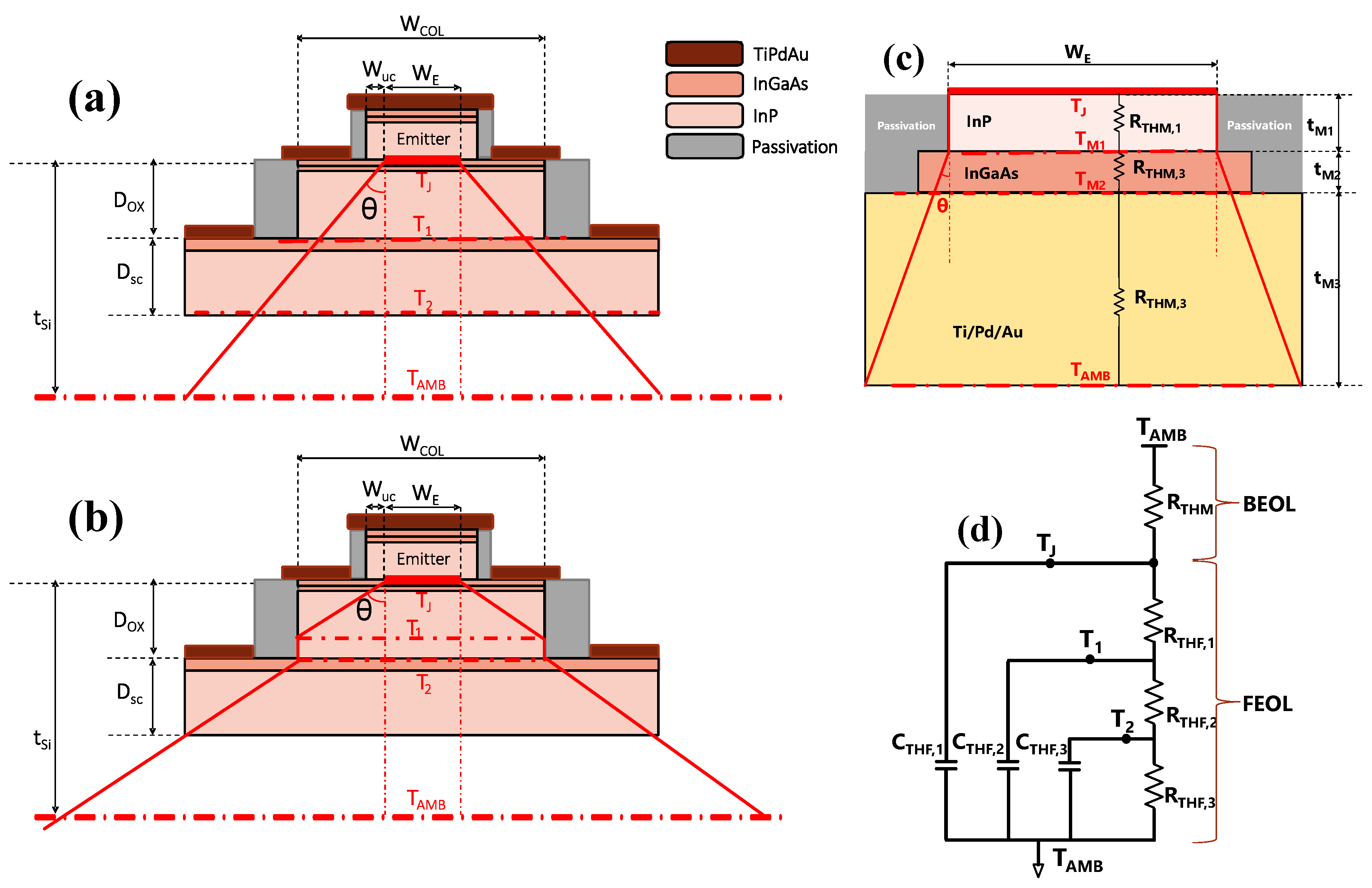
5.1. Dynamic Self-Heating and Thermal Impedance Modeling in InP DHBTs
5.1.1. Thermal Impedance Extraction Method from Low-Frequency S-Parameters
5.1.2. Geometry Scalable Thermal Impedance Model
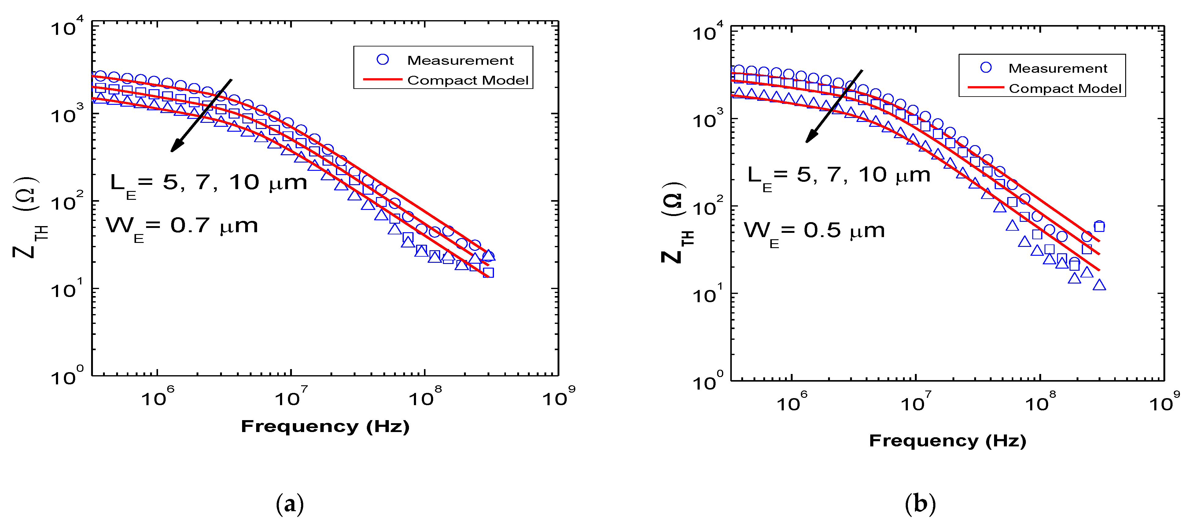
5.1.3. Thermal Impedance (ZTH) Extraction and Model Validation
5.2. Thermal Characterization and Modeling of UTC Photodiodes
6. High Frequency Characterization and Modelling
6.1. High Frequency Characterization of InP DHBTs
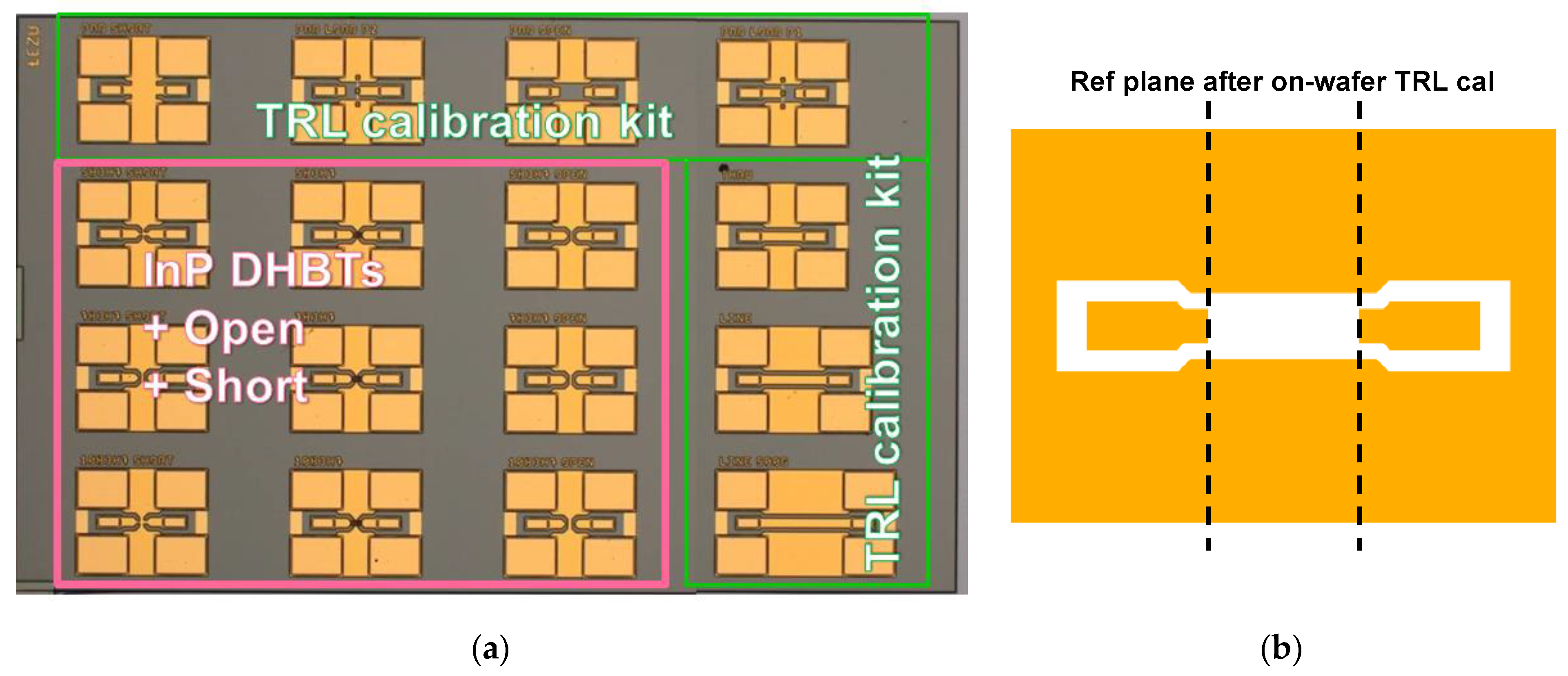
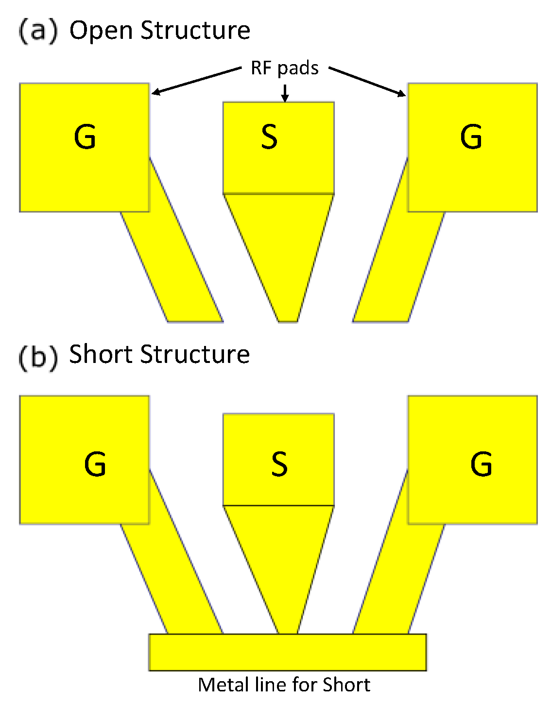
6.1.1. Dedicated Test Structure Design
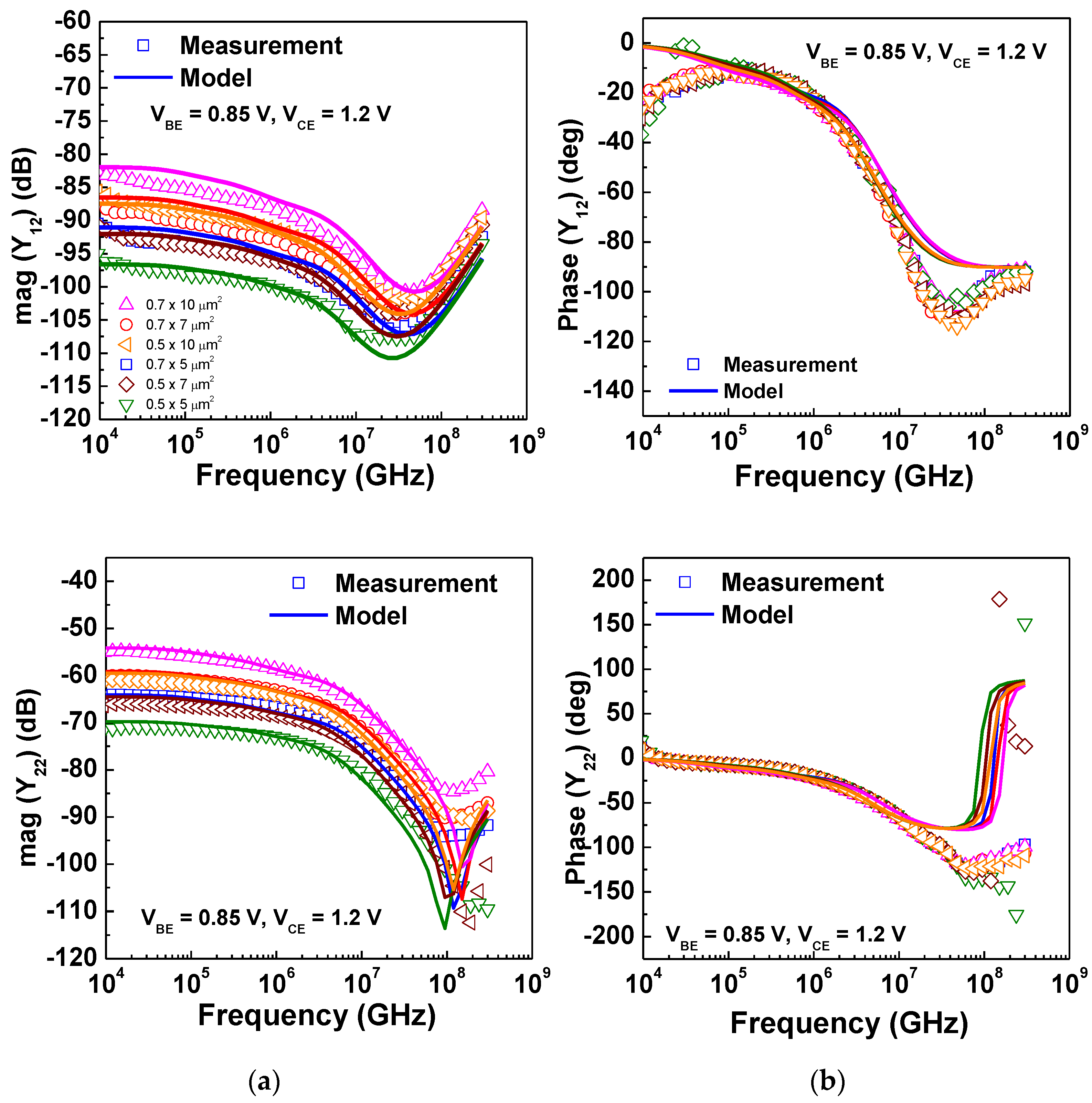
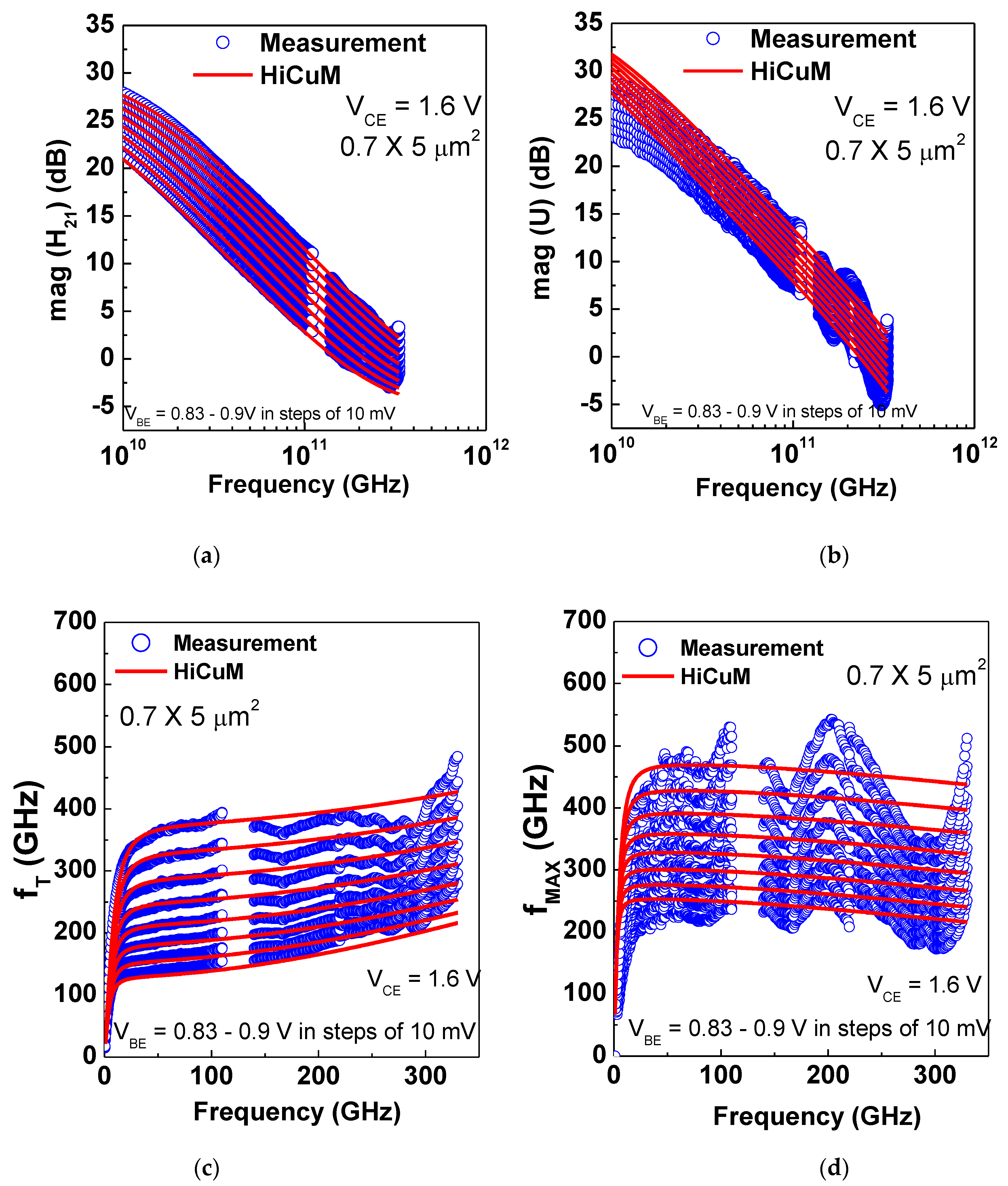
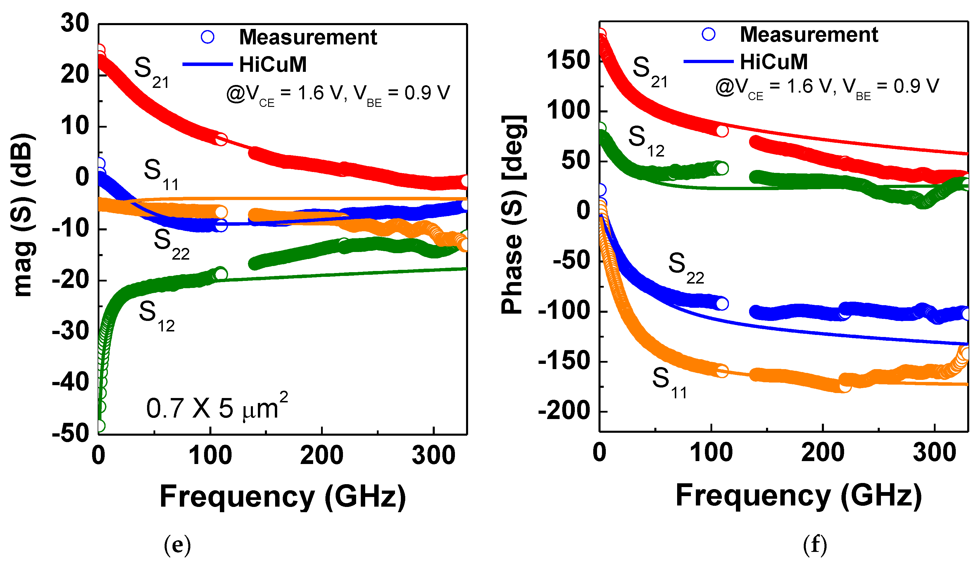
6.1.2. Measurement Results and HiCuM Compact Model Validation Up to 330 GHz
6.2. High-Frequency Characterization of UTC Photodiodes
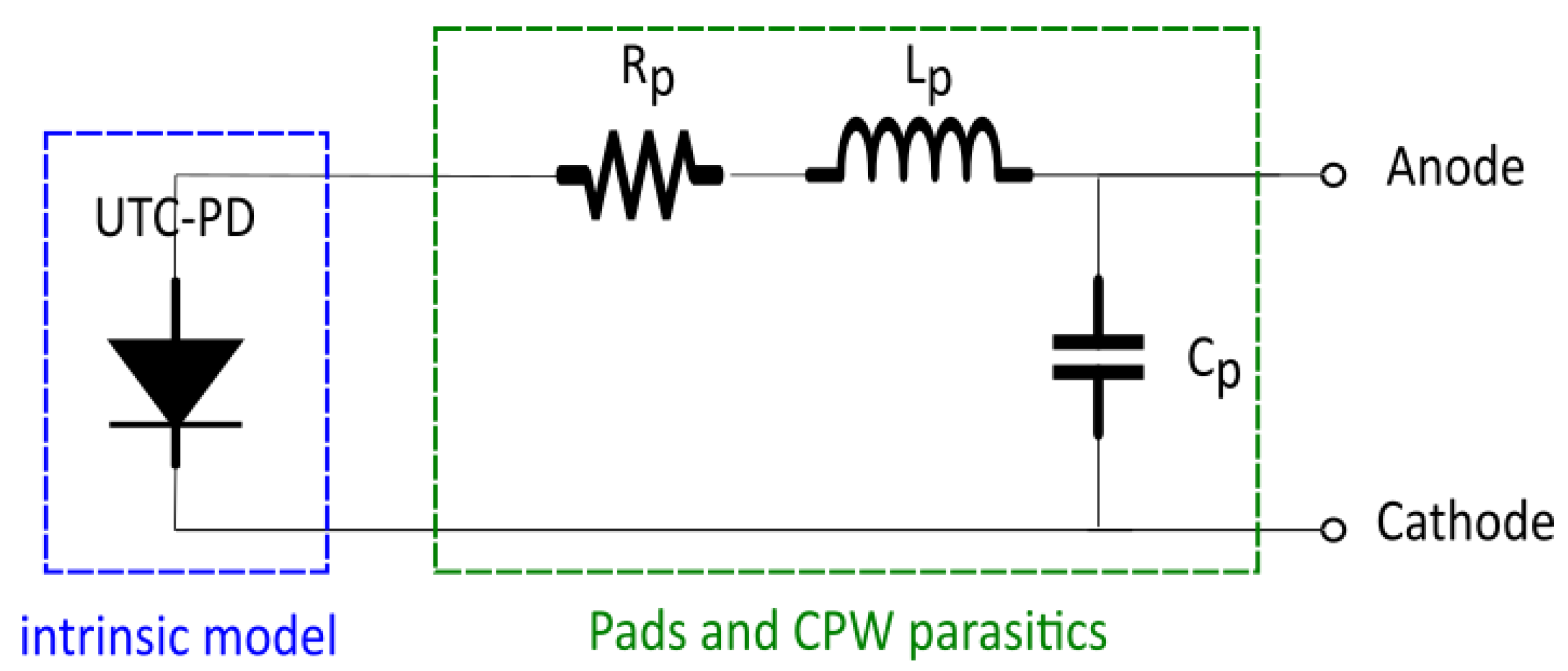
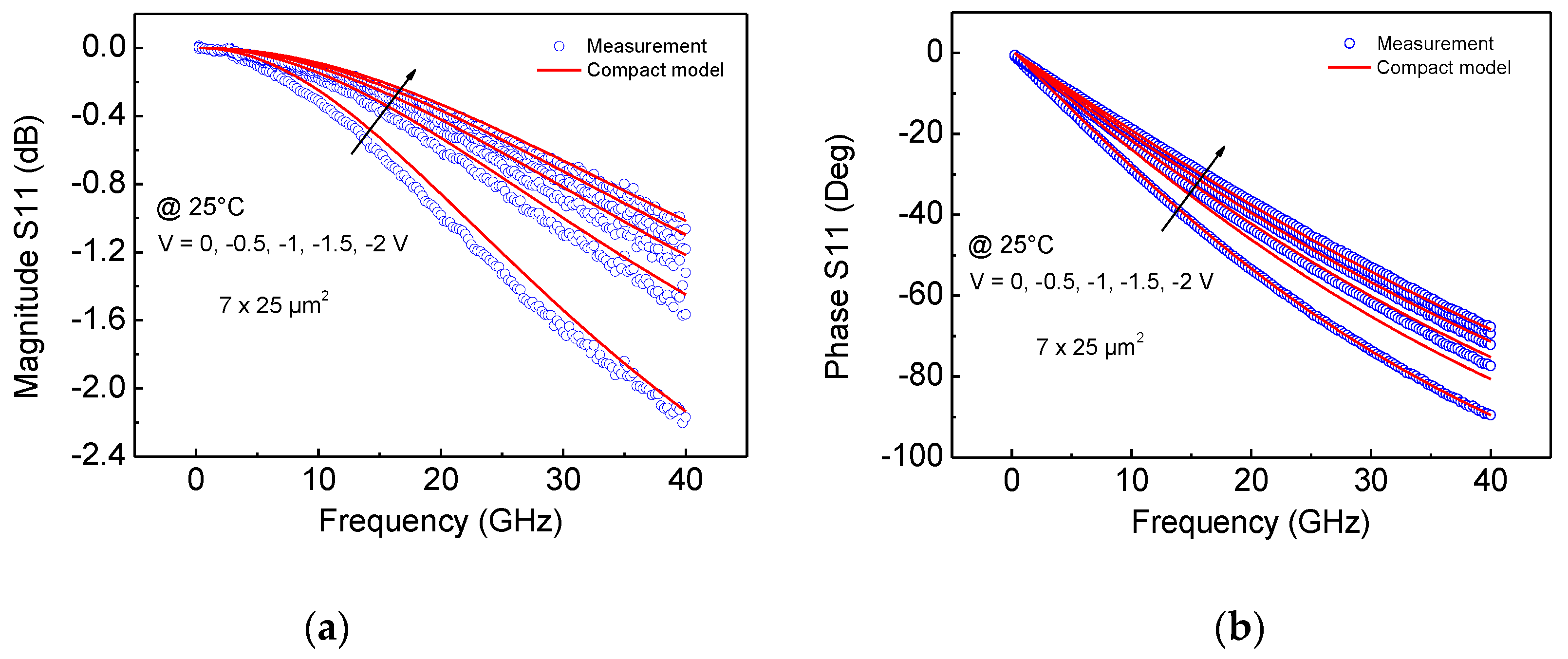
6.2.1. Extrinsic Elements
6.2.2. De-Embedding (Extraction of Parasitic Elements)
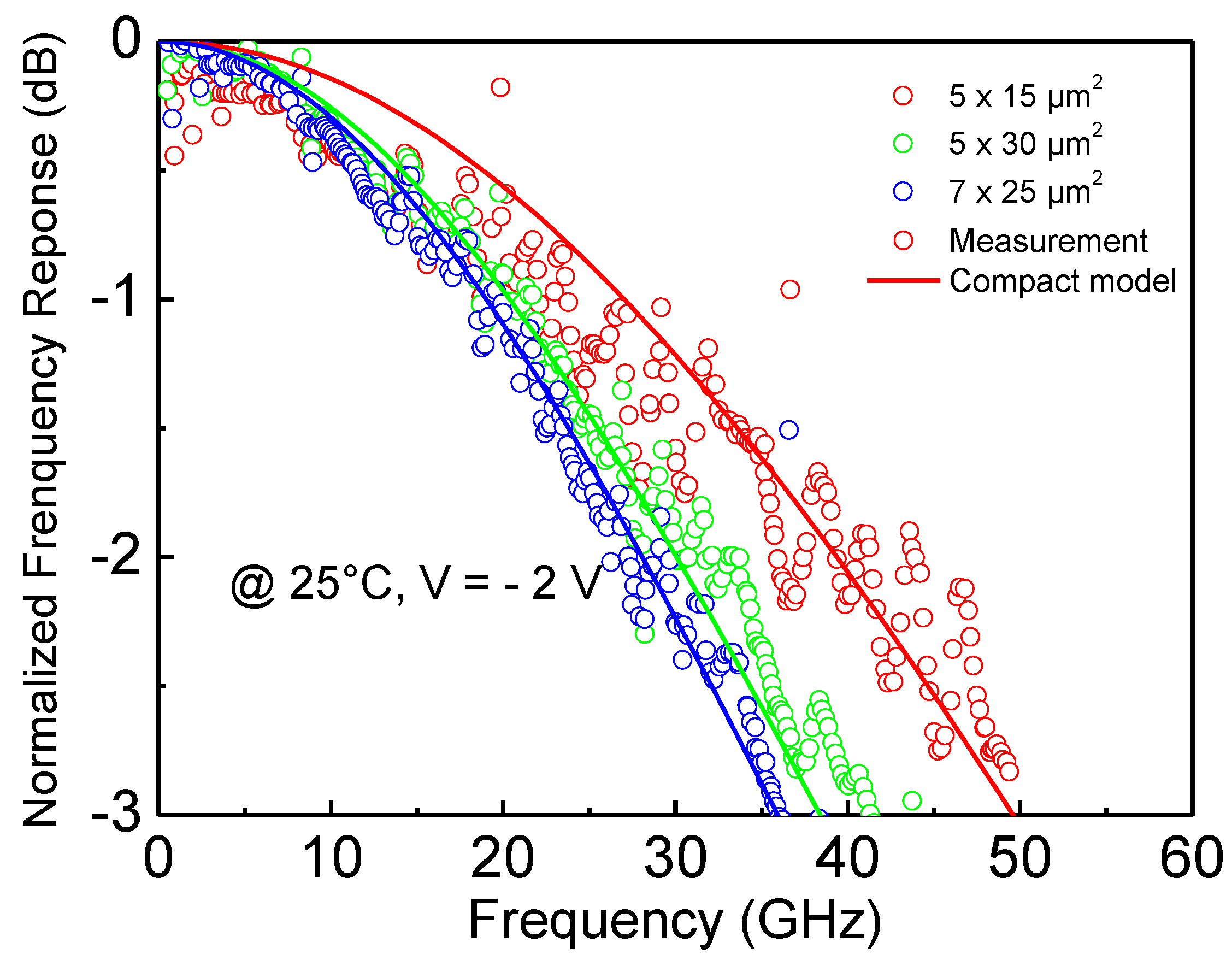
6.2.3. Optical Frequency Response
7. Co-Simulation for Design of Future Electronic–Photonic Integrated Circuits and Performance Prediction
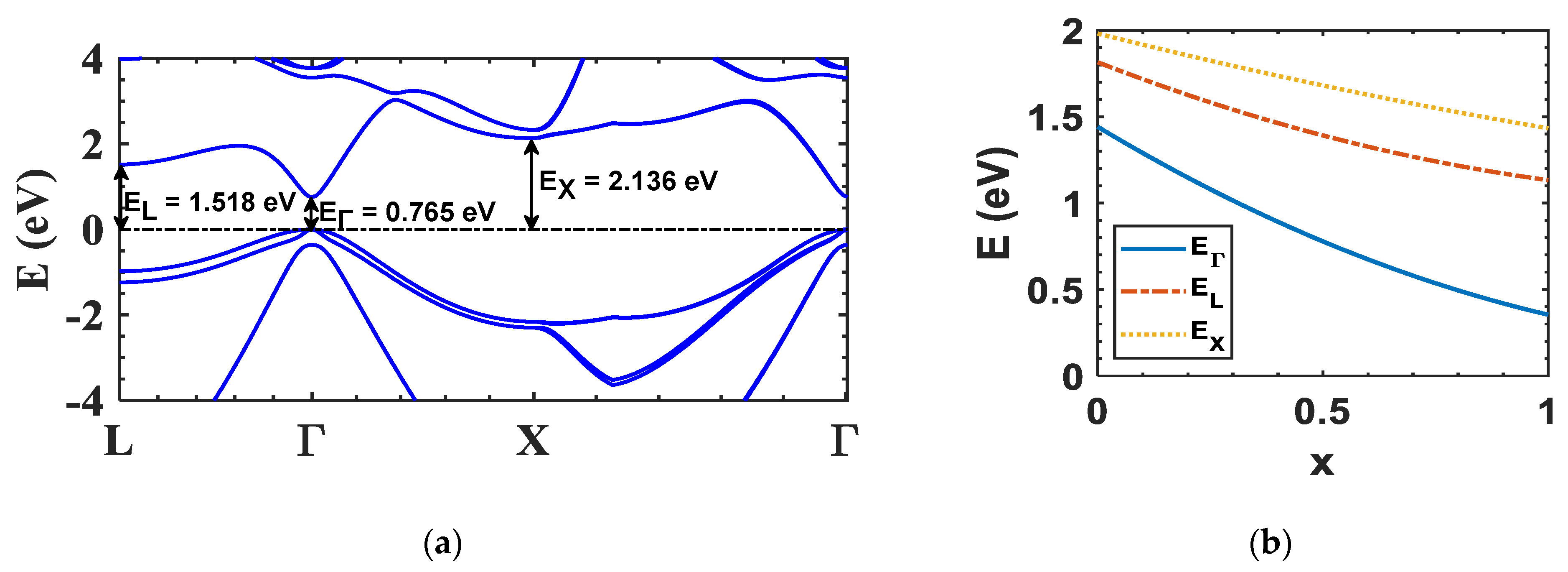
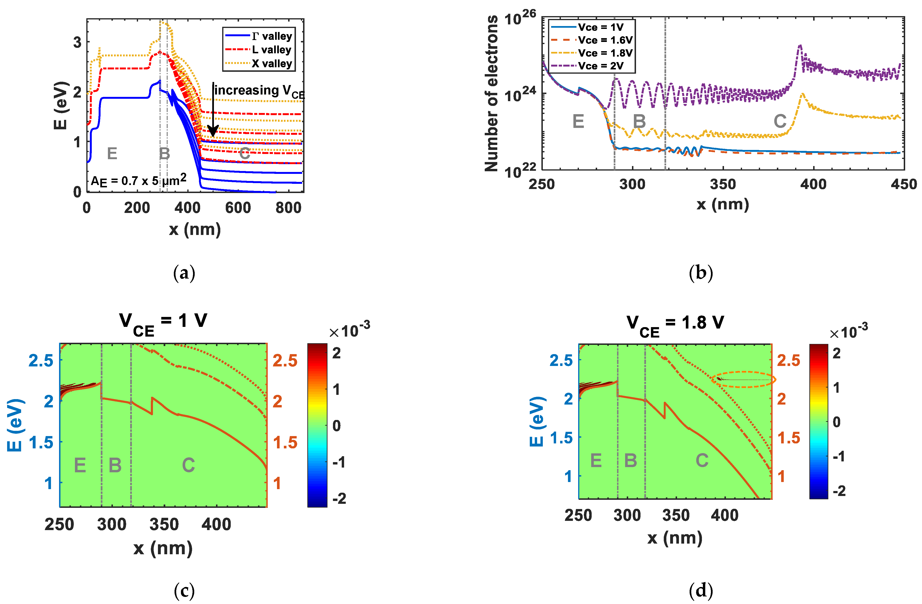
7.1. TCAD and Monte Carlo Simulations
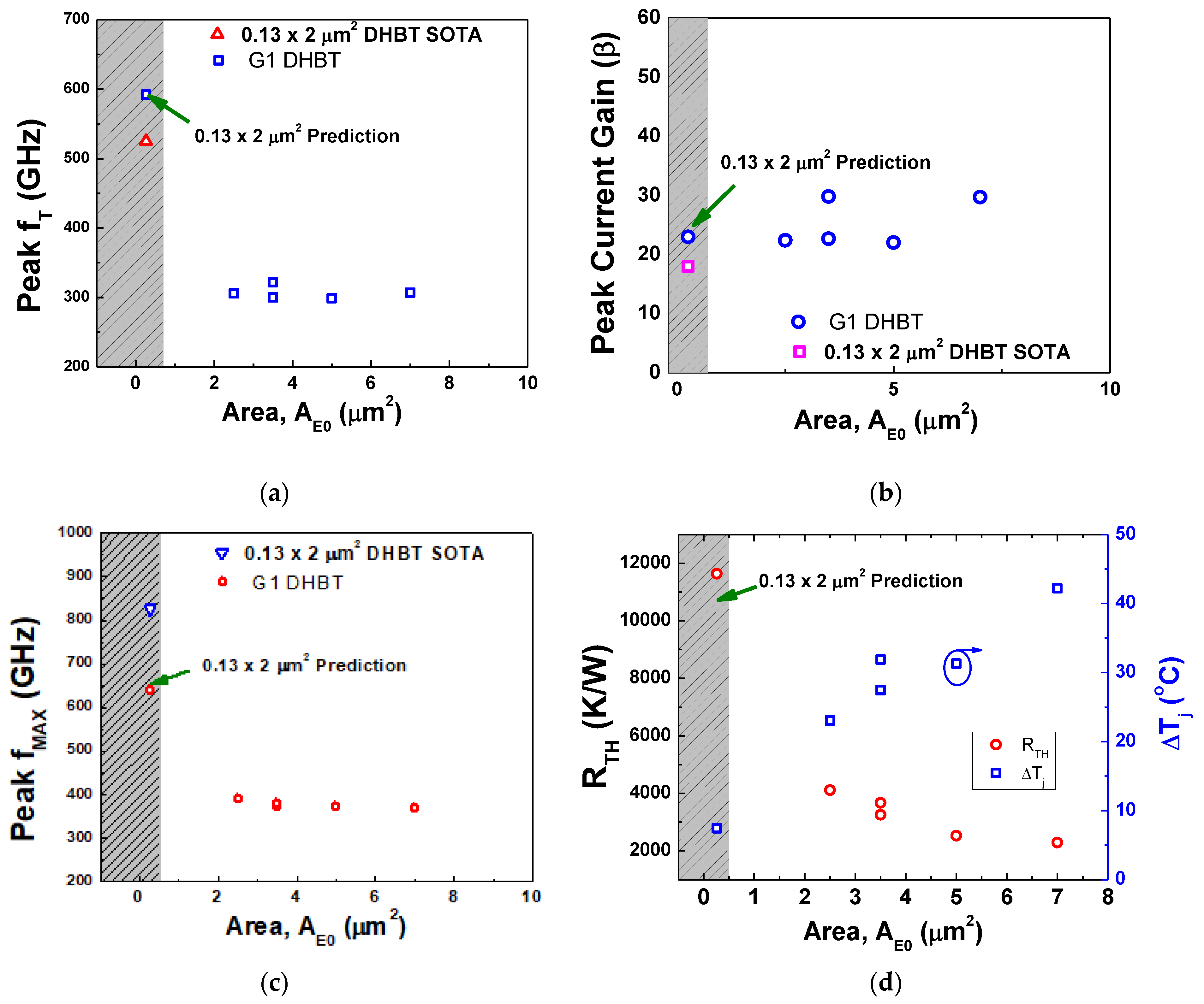
7.2. Extrapolation of Figures of Merits to State-of-the-Art (0.13 × 2 μm2) DHBTs Using Compact Model
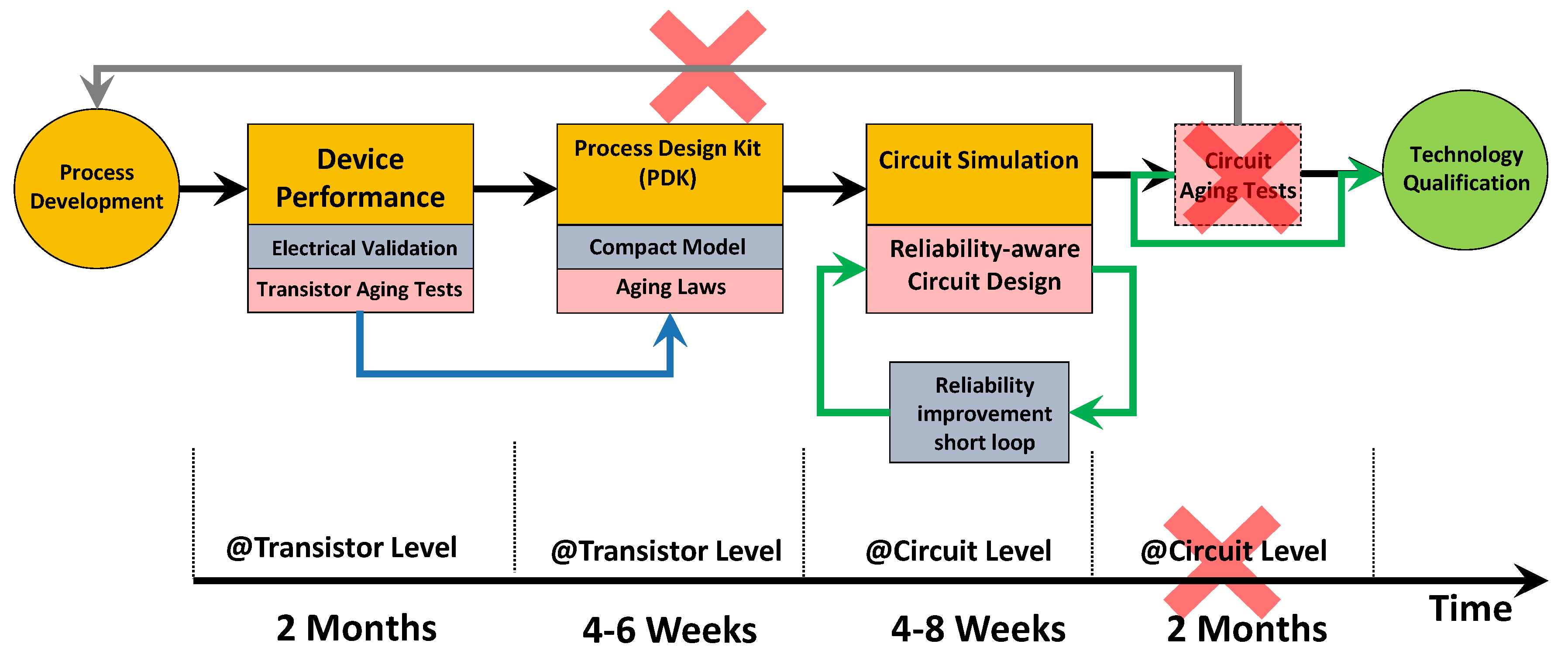
7.3. Toward a Reliability-Aware Design Framework
8. Conclusions
Author Contributions
Funding
Conflicts of Interest
References
- Urteaga, M.; Griffith, Z.; Seo, M.; Hacker, J.; Rodwell, M.J. InP HBT Technologies for THz Integrated Circuits. Proc. IEEE 2017, 105, 1051–1067. [Google Scholar] [CrossRef]
- Ishibashi, T.; Furata, T.; Fushimi, H.; Kodama, S.; Ito, H.; Nagatsuma, T.; Shimizu, N.; Miyamoto, Y. InP/InGaAs Uni-Travelling-Carrier Photodiodes. IEICE Trans. Electron. 2000, 83, 938–949. [Google Scholar]
- Ishibashi, T.; Shimizu, N.; Kodama, S.; Ito, H.; Nagatsuma, T.; Furata, H. Uni-Travelling-Carrier Photodiodes. Tech. Dig., Ultrafast Electronics and Optoelectronics. In Proceedings of the OSA Spring Topical Meeting, Nevada, USA, 17–21 March 1997; pp. 166–168. [Google Scholar]
- Ito, H.; Nagatsuma, T.; Hirata, A.; Minotani, T.; Sasaki, A.; Hirota, Y.; Lshibashi, T. High-power photonic millimeter wave generation at 100GHz using matching-circuit-integrated uni-travelling-carrier photodiodes. IEE Proc. Optoelectron. 2003, 150, 138. [Google Scholar] [CrossRef]
- Ito, H.; Furuta, T.; Ito, T.; Muramoto, Y.; Tsuzuki, K.; Yoshino, K.; Ishibashi, T. W-band uni-travelling-carrier photodiode module for high-power photonic millimeter wave generation. Electron. Lett. 2002, 38, 1376–1377. [Google Scholar] [CrossRef]
- Nagatsuma, T. 300-GHz-band Wireless Communications with High-power Photonic Sources. In Proceedings of the 2014 XXXIth URSI General Assembly and Scientific Symposium (URSI GASS), Beijing, China, 16–23 August 2014. [Google Scholar] [CrossRef]
- Ishibashi, T.; Muramoto, Y.; Yoshimatsu, T.; Ito, H. Continuous THz Wave Generation by Photodiodes up to 2.5 THz. In Proceedings of the International Conference on Infrared, Millimeter, and Terahertz Waves, IRMMW-THz, Mainz, Germany, 1–6 September 2013. [Google Scholar] [CrossRef]
- Kanno, A.; Dat, P.T.; Sekine, N.; Osako, I.; Yamamoto, N.; Yoshida, Y.; Kitayama, K.-I.; Kawanishi, T. Seamless Fiber-Wireless Bridge in the millimeter- and Terahertz-Wave Bands. J. Lightwave Technol. 2016, 34, 4794–4801. [Google Scholar] [CrossRef]
- Nodjiadjim, V.; Riet, M.; Mismer, C.; Hersent, R.; Jorge, F.; Konczykowska, A.; Dupuy, J.-Y. 0.7-μm InP DHBT technology with 400-GHz fT and fMAX and 4.5-V BVCE0 for high speed and high frequency integrated circuits. IEEE J. Electron Devices Soc. 2019, 7, 748–752. [Google Scholar] [CrossRef]
- Achouche, M.; Magnin, V.; Harari, J.; Lelarge, F.; Derouin, E.; Jany, C.; Carpentier, D.; Blache, F.; Decoster, D. High Performance Evanescent Edge Coupled Waveguide Unitraveling-Carrier Photodiodes for >40-Gb/s Optical Receivers. IEEE Photonics Technol. Lett. 2004, 16, 584–586. [Google Scholar] [CrossRef]
- Magnin, V.; Giraudet, L.; Harari, J.; Decobert, J.; Pagnot, P.; Boucherez, E.; Decoster, D. Design, Optimization, and Fabrication of Side-Illuminated p-i-n Photodetectors With High Responsivity and High Alignment Tolerance for 1.3- and 1.55-m Wavelength Use. J. Lightwave Technol. 2002, 20, 477–488. [Google Scholar] [CrossRef]
- Schröter, M.; Chakravorty, A. Compact Hierarchical Bipolar Transistor Modeling with HiCUM; International Series on Advances in Solid State Electronics and Technology; World Scientific: Singapore, 2010. [Google Scholar]
- Mukherjee, C.; Natrella, M.; Seddon, J.; Graham, C.; Mounaix, P.; Renaud, C.C.; Maneux, C. Efficient compact modelling of UTC-photodiode towards terahertz communication system design. Solid-State Electron. 2020, 170, 107836. [Google Scholar] [CrossRef]
- Mukherjee, C.; Couret, M.; Nodjiadjim, V.; Riet, M.; Dupuy, J.-Y.; Fregonese, S.; Zimmer, T.; Maneux, C. Scalable Modeling of Thermal Impedance in InP DHBTs Targeting Terahertz Applications. IEEE Trans. Electron Devices 2019, 66, 2125–2131. [Google Scholar] [CrossRef] [Green Version]
- Scholten, A.J.; Smit, G.D.J.; Durand, M.; van Langevelde, R.; Klaassen, D.B.M. The Physical Background of JUNCAP2. IEEE Trans. Electron Devices 2006, 53, 2098–2107. [Google Scholar] [CrossRef]
- Verdun, M.; Beaudoin, G.; Portier, B.; Bardou, N.; Dupuis, C.; Sagnes, I.; Haïdar, R.; Pardo, F.; Pelouard, J.-L. Dark current investigation in thin P-i-N InGaAs photodiodes for nano-resonators. J. Appl. Phys. 2016, 120, 084501. [Google Scholar] [CrossRef] [Green Version]
- Ishibashi, T.; Ito, H. Uni-traveling-carrier photodiodes. J. Appl. Phys. 2020, 127, 031101. [Google Scholar] [CrossRef]
- Huszka, Z.; Nidhin, K.; Céli, D.; Chakravorty, A. Extraction of Compact Static Thermal Model Parameters for SiGe HBTs. IEEE Trans. Electron Devices 2021, 68, 491–496. [Google Scholar] [CrossRef]
- Couret, M.; Fischer, G.; Frégonése, S.; Zimmer, T.; Maneux, C. Physical, small-signal and pulsed thermal impedance characterization of multi-finger SiGe HBTs close to the SOA edges. In Proceedings of the 2019 IEEE 32nd International Conference on Microelectronic Test Structures (ICMTS), Kita-Kyushu City, Fukuoka, Japan, 18–21 March 2019; pp. 154–159. [Google Scholar] [CrossRef] [Green Version]
- Kone, G.A.; Grandchamp, B.; Hainaut, C.; Marc, F.; Labat, N.; Zimmer, T.; Nodjiadjim, V.; Riet, M.; Dupuy, J.; Godin, J.; et al. Submicrometer InP/InGaAs DHBT Architecture Enhancements Targeting Reliability Improvements. IEEE Trans. Electron Devices 2013, 60, 1068–1074. [Google Scholar] [CrossRef]
- Grandchamp, B.; Nodjiadjim, V.; Zaknoune, M.; Koné, G.A.; Hainaut, C.; Godin, J.; Riet, M.; Zimmer, T.; Maneux, C. Trends in Submicrometer InP-Based HBTArchitecture Targeting Thermal Management. IEEE Trans. Electron Devices 2011, 58, 2566–2572. [Google Scholar] [CrossRef]
- Kiuru, T.; Mallat, J.; Raisanen, A.V.; Narhi, T. Schottky diode series resistance and thermal resistance extraction from S -parameter and temperature controlled I–V measurements. IEEE Trans. Microw. Theory Tech. 2011, 59, 2108–2116. [Google Scholar] [CrossRef]
- Fregonese, S.; de Matos, M.; Deng, M.; Potereau, M.; Ayela, C.; Aufinger, K.; Zimmer, T. On-wafer characterization of silicon transistors up to 500 GHz and analysis of measurement discontinuities between the frequency bands. IEEE Trans. Microw. Theory Tech. 2018, 66, 3332–3341. [Google Scholar] [CrossRef] [Green Version]
- Yau, K.; Dacquay, E.; Sarkas, I.; Voinigescu, S. Device and IC characterization above 100 GHz. IEEE Microw. Mag. 2012, 13, 30–54. [Google Scholar] [CrossRef]
- Deng, M.; Mukherjee, C.; Yadav, C.; Fregonese, S.; Zimmer, T.; Matos, M.D.; Quan, W.; Arabhavi, A.M.; Bolognesi, C.R.; Wen, X.; et al. Design of On-Wafer TRL Calibration Kit for InP Technologies Characterization up to 500 GHz. IEEE Trans. Electron Devices 2020, 67, 5441–5447. [Google Scholar] [CrossRef]
- Wen, X.; Mukherjee, C.; Raya, C.; Ardouin, B.; Deng, M.; Frégonèse, S.; Nodjiadjim, V.; Riet, M.; Quan, W.; Arabhavi, A.M.; et al. A multiscale TCAD approach for the simulation of InP DHBTs and the extraction of their transit times. IEEE. Trans. Electron Devices 2019, 66, 5084–8090. [Google Scholar] [CrossRef]
- Luisier, M.; Schenk, A.; Fichtner, W.; Klimeck, G. Atomistic simulation of nanowires in the sp3d5s∗ tight-binding formalism: From boundary conditions to strain calculations. Phys. Rev. B 2006, 74, 205323. [Google Scholar] [CrossRef] [Green Version]
- Sentaurus Device; v.J-2015.06; Synopsys Inc.: Mountain View, CA, USA, 2015.
- Vurgaftman, I.; Meyer, J.R.; Ram-Mohan, L.R. Band parameters for III–V compound semiconductors and their alloys. J. Appl. Phys. 2001, 89, 5815–5875. [Google Scholar] [CrossRef] [Green Version]
- Yngvesson, S. Microwave Semiconductor Devices; Springer Science & Business Media: Berlin, Germany, 1991. [Google Scholar]
- Rodwell, M.J.W.; Le, M.; Brar, B. InP Bipolar ICs: Scaling Roadmaps, Frequency Limits, Manufacturable Technologies. Proc. IEEE 2008, 96, 271–286. [Google Scholar] [CrossRef]
- Schröter, M.; Rosenbaum, T.; Chevalier, P.; Heinemann, B.; Voinigescu, S.P.; Preisler, E.; Böck, J.; Mukherjee, A. SiGe HBT Technology: Future Trends and TCAD-Based Roadmap. Proc. IEEE 2017, 105, 1068–1086. [Google Scholar] [CrossRef]
- Urteaga, M.; Pierson, R.; Rowell, P.; Jain, V.; Lobisser, E.; Rodwell, M.J.W. 130 nm InP DHBTs with ft >0.52THz and fmax >1.1THz. In Proceedings of the 69th Device Research Conference, Santa Barbara, CA, USA, 20–22 June 2011; pp. 281–282. [Google Scholar]
- Mukherjee, C.; Raya, C.; Ardouin, B.; Deng, M.; Frégonèse, S.; Zimmer, T.; Nodjiadjim, V.; Riet, M.; Dupuy, J.Y.; Luisier, M.; et al. Scalable Compact Modeling of III–V DHBTs: Prospective Figures of Merit Toward Terahertz Operation. IEEE Trans. Electron Devices 2018, 65, 5357–5364. [Google Scholar] [CrossRef]
- Thiam, A.; Roelens, Y.; Coinon, C.; Avramovic, V.; Grandchamp, B.; Ducatteau, D.; Wallart, X.; Maneux, C.; Zaknoune, M. InP HBT thermal management by transferring to high thermal conductivity silicon substrate. IEEE Electron Device Lett. 2014, 35, 1010–1012. [Google Scholar] [CrossRef]
- Shiratori, Y.; Hoshi, T.; Ida, M.; Higurashi, E.; Matsuzaki, H. High-speed InP/InGaAsSb DHBT on high-thermal-conductivity SiC substrate. IEEE Electron Device Lett. 2018, 39, 807–810. [Google Scholar] [CrossRef]
- Quan, W.; Arabhavi, M.A.; Flückiger, R.; Ostinelli, O.; Bolognesi, C.R. Quaternary graded-base InP/GaInAsSb DHBTs with fT /fMAX = 547/784 GHz. IEEE Electron Dev. Lett. 2018, 39, 1141–1144. [Google Scholar] [CrossRef]
- Nagatsuma, T.; Ducournau, G.; Renaud, C.C. Advances in terahertz communications accelerated by photonics. Nat. Photon 2016, 10, 371–379. [Google Scholar] [CrossRef]
- Pavanello, F. Uni-Travelling Carrier Photodiodes and Metal Mesh Filters Based on SUB-wavelength Apertures for THz Applications. Ph.D. Thesis, Université Lille, Lille, France, 2013. [Google Scholar]
- Chevalier, P.; Schröter, M.; Bolognesi, C.R.; d’Alessandro, V.; Alexandrova, M.; Böck, J.; Flückiger, R.; Fregonese, S.; Heinemann, B.; Jungemann, C.; et al. Si/SiGe:C and InP/GaAsSb Heterojunction Bipolar Transistors for THz Applications. Proc. IEEE 2017, 105, 1035–1050. [Google Scholar] [CrossRef]
- Mukherjee, C.; Ardouin, B.; Dupuy, J.-Y.; Nodjiadjim, V.; Riet, M.; Zimmer, T.; Marc, F.; Maneux, C. Reliability-Aware Circuit Design Methodology for Beyond-5G Communication Systems. IEEE Trans. Device Mater. Reliab. 2017, 17, 490–506. [Google Scholar] [CrossRef] [Green Version]
- Fregonese, S.; Cabbia, M.; Yadav, C.; Deng, M.; Panda, S.R.; de Matos, M.; Céli, D.; Chakravorty, A.; Zimmer, T. Analysis of High-Frequency Measurement of Transistors Along with Electromagnetic and SPICE Cosimulation. IEEE Trans. Electron Devices 2020, 67, 4770–4776. [Google Scholar] [CrossRef]


| Device Area (µm2) | 0.5 × 5 | 0.5 × 7 | 0.5 × 10 | 0.7 × 5 | 0.7 × 7 | 0.7 × 10 |
|---|---|---|---|---|---|---|
| RTH1 (K/W) | 3680 | 2910 | 1980 | 2714 | 1865 | 1456 |
| RTH2 (K/W) | 1195 | 1095 | 777 | 1297 | 1108 | 856 |
| RTH3 (K/W) | 920 | 768 | 680 | 868 | 825 | 773 |
| CTH1 (pJ/K) | 12.5 | 17 | 29 | 21 | 28 | 43 |
| CTH2 (pJ/K) | 140 | 215 | 320 | 165 | 220 | 340 |
| CTH3 (nJ/K) | 1.75 | 1.9 | 2.23 | 1.9 | 2.13 | 2.45 |
| Device Area (µm2) | 0.5 × 5 | 0.5 × 7 | 0.5 × 10 | 0.7 × 5 | 0.7 × 7 | 0.7 × 10 |
|---|---|---|---|---|---|---|
| RTHF (K/W) | 5795 | 4773 | 3437 | 4879 | 3798 | 3085 |
| RTHM (K/W) | 17,500 | 12,050 | 9800 | 11,050 | 9250 | 6960 |
| RTH (model) (K/W) | 4353 | 3418 | 2544.6 | 3384 | 2687 | 2137 |
| RTH (measured) (K/W) | 4114 | 3257 | 2526 | 3675 | 2720 | 2289 |
| Dimensions. | Parameters | Model | Standard Deviation | RTh (K/W) |
|---|---|---|---|---|
| 5 × 15 µm2 | R(Ω) | 60.58 | ±2 | 1013 |
| Is(A) | 4.6 × 10⁻¹² | ±0.4 × 10⁻¹² | ||
| N | 1.365 | ±0 | ||
| 5 × 30 µm2 | R(Ω) | 36.31 | ±5 | 844 |
| Is(A) | 8.77 × 10⁻¹² | ±0.07 × 10⁻¹² | ||
| N | 1.363 | ±0 | ||
| 7 × 25 µm2 | R(Ω) | 27.7 | ±2 | 612 |
| Is(A) | 6.6 × 10⁻¹² | ±0.1 × 10⁻¹² | ||
| N | 1.360 | ±0.03 |
| Cp (fF) | Lp (pH) | Rp (Ω) |
|---|---|---|
| 26 | 61.5 | 1.5 |
Publisher’s Note: MDPI stays neutral with regard to jurisdictional claims in published maps and institutional affiliations. |
© 2021 by the authors. Licensee MDPI, Basel, Switzerland. This article is an open access article distributed under the terms and conditions of the Creative Commons Attribution (CC BY) license (http://creativecommons.org/licenses/by/4.0/).
Share and Cite
Mukherjee, C.; Deng, M.; Nodjiadjim, V.; Riet, M.; Mismer, C.; Guendouz, D.; Caillaud, C.; Bertin, H.; Vaissiere, N.; Luisier, M.; et al. Towards Monolithic Indium Phosphide (InP)-Based Electronic Photonic Technologies for beyond 5G Communication Systems. Appl. Sci. 2021, 11, 2393. https://0-doi-org.brum.beds.ac.uk/10.3390/app11052393
Mukherjee C, Deng M, Nodjiadjim V, Riet M, Mismer C, Guendouz D, Caillaud C, Bertin H, Vaissiere N, Luisier M, et al. Towards Monolithic Indium Phosphide (InP)-Based Electronic Photonic Technologies for beyond 5G Communication Systems. Applied Sciences. 2021; 11(5):2393. https://0-doi-org.brum.beds.ac.uk/10.3390/app11052393
Chicago/Turabian StyleMukherjee, Chhandak, Marina Deng, Virginie Nodjiadjim, Muriel Riet, Colin Mismer, Djeber Guendouz, Christophe Caillaud, Hervé Bertin, Nicolas Vaissiere, Mathieu Luisier, and et al. 2021. "Towards Monolithic Indium Phosphide (InP)-Based Electronic Photonic Technologies for beyond 5G Communication Systems" Applied Sciences 11, no. 5: 2393. https://0-doi-org.brum.beds.ac.uk/10.3390/app11052393