Article

Nano Scaled Checkerboards: A Long Range Ordering in NiCoMnAl Magnetic Shape Memory Alloy Thin Films with Martensitic Intercalations

Thin Films and Physics of Nanostructures, Physics Department, Bielefeld University, P.O. Box 100131, 33501 Bielefeld, Germany
*
Author to whom correspondence should be addressed.
Submission received: 7 January 2022 / Revised: 2 February 2022 / Accepted: 4 February 2022 / Published: 8 February 2022
(This article belongs to the Special Issue Advances in Magnetic Nanomaterials and Nanostructures)

Abstract

:
Magnetic shape memory Heusler alloys, such as NiCoMnAl, are considered as promising candidates for magnetocaloric cooling applications. Grown in thin film systems of adjacent layers with austenite and martensite crystal structures of almost equal thicknesses, a long-range ordering phenomenon in the shape of a 3D checkerboard pattern occurs in NiCoMnAl samples. The crystallographic origin of the pattern is proven by transmission electron microscopy (TEM) techniques. The darker fields of the arrangement consist of martensite nuclei superposed with austenite, while the purely austenite regions appear bright in TEM cross sections. The nucleation process is presumably triggered by inhomogeneous local elastic stray fields of primary martensitic nuclei in the austenite matrix and limited by the thicknesses of the martensite and austenite thin films.

1. Introduction

Shape memory alloys reveal the fascinating ability to recover their initial shape after deformation upon heating. Therefore, their electrical and thermal properties depend strongly on temperature and mechanical stress, which opens different fields of applications [1,2]. Their functional abilities originate in a temperature induced phase transition, known as martensitic transformation, between two crystal structures: the high-temperature austenite and the low-temperature martensite phase. The discovery of the shape memory effect in ferromagnetic Ni2MnGa by Ullakko et al. in 1996 [3], offers new application fields of shape memory alloys, because the martensitic transition cannot only be triggered by temperature, mechanical strain or hydrostatic pressure but also by external magnetic fields [4,5,6,7]. This so-called magnetic shape memory effect, e.g., allows much higher cycling frequencies of the phase transition compared to conventional thermally driven shape memory alloys, which are limited due to the thermal transport [8,9]. A special class of magnetic shape memory alloys are Heusler compounds such as NiMnX (X = Al, Ga, Sn, In), which are considered as promising materials for magnetocaloric cooling applications due to their magnetoelastic coupling near room temperature [10,11,12]. However, most of the compounds show a large thermal hysteresis, which limits their potential in future applications [13,14,15]. Therefore, efficient mechanisms to change the martensitic transformation behavior have to be identified. In literature different approaches can be found to solve this issue ranging from the improvement of the chemical composition of the chosen material [16], the enhancement of the compatibility between martensitic and austenitic phase by applying a hydrostatic pressure [17] to just using the minor loops of the thermal hysteresis [18].
In a previous study, we have demonstrated that the thermal hysteresis could be decreased by preparing off-stoichiometric NiCoMnAl multilayer systems, which consist of alternating grown martensite intercalations (MIs) and active transforming austenitic layers (ALs) [19]. This MIs have shown to be beneficial for transforming films, because the formation energy during martensite nucleation is reduced. The temperature dependent magnetization measurements have shown a significant decrease in hysteresis width as a function of the number of MIs. If the austenite active layers have a similar thickness compared to the martensite intercalations an extraordinary microstructure has been visualized in cross section images [19].
Independently from the considered material, the applied treatment or the scale of the investigated structure, it is well known that the microstructure has a great impact on materials properties such as magnetic, electronic or mechanical behavior [20,21,22,23,24,25,26]. Therefore, effects of the observed structure on the properties of the shape memory alloy can be expected, but little is known about this novel structure so far. In the present study we investigate the microstructure of the arrangement by transmission electron microscopy (TEM) in terms of crystallinity, temperature dependence, influence of layer thicknesses and discuss its physical origin.

2. Materials and Methods

The NiCoMnAl thin film systems have been prepared by magnetron co-sputtering from pure elemental Ni, Mn, Al and Co targets. DC and RF sources were used for this process from 3-inch targets of Ni (DC), Mn (DC), Al (DC) and Co (RF) with a purity of 4N. MgO (001) substrates were used, because the low lattice mismatch between the substrate, the V seed layer and NiCoMnAl allows an epitaxial growth of the Heusler compound.
Prior to deposition the MgO substrate was heated up to (723 ± 35) K. The base pressure in the deposition chamber was better than 5 × 10⁻⁹ mbar and the distance between target and substrate was 21 cm. To compensate a non-uniform deposition, the substrate is rotated constantly with a speed of 10 rpm. Due to the experience from previous studies, a 30 nm thick V seed layer was deposited on the MgO to improve the martensitic transformation [27]. NiCoMnAl multilayer systems with alternating martensite intercalations and active transforming austenitic layers have been prepared. The stoichiometry of the compound in these two layers is chosen in such a way that their individual thermal hysteresis does not overlap, as depicted in Figure 1a. More details about the transition temperatures and the measured thermal hysteresis can be found in our previous study [19]. An illustration of the initially sputtered multilayer system is given in Figure 1b. The sample has 50 nm thick ALs with the composition Ni43Co7Mn31Al19 and 30 nm thick Ni47Co3Mn33Al17 as MIs with overall 13 iterations. The nominal compositions were derived from the individual deposition rates of the elemental targets by changing the energy of the target source. The deposition rates were calibrated per source before each batch of samples, which enable film thickness errors of less than 3% within a batch. For the investigation of dependence of the arrangement on the layer thicknesses, samples with only 6 martensitic intercalations have been prepared. Immediately after deposition all samples were cooled to room temperature in order to minimize diffusion processes and a capping layer of 2 nm Ru was deposited to prevent from oxidation.
Cross section samples have been prepared by focused ion beam (FIB) cutting along the [110]MgO-direction. Here, we used a FEI Helios Dual Beam FIB with 30 kV Ga+-ions for beam milling and 5 kV Ga+-ions for the polishing step. For analytical transmission electron microscopy (TEM) a JEOL JEM-2200FS and a JEOL JEM-ARM200F, both operated at 200 kV, have been employed. The TEMs are equipped with EDX detectors used for elemental mappings. The microstructure has been determined by selected area electron diffraction (SAED) or Fast Fourier Transformation (FFT) of high-resolution images. For the simulation of diffraction and TEM images the software QSTEM has been employed. Its subprogram gbmaker has been used for creating the crystal structure including the random site placement of Ni/Co respective Mn/Al [28]. X-ray diffraction (XRD) measurements have been performed using a Phillips X’Pert Pro MPD diffractometer equipped with a Cu anode and operated in Bragg-Brentano geometry.

3. Results

A long-range ordering phenomenon can be observed in NiCoMnAl multilayer systems as can be seen in Figure 2a,b. The intended layered structure is cancelled, and transformed into a checkerboard-like periodic arrangement of darker and brighter areas. The pattern consists of three types of fields: big quadratic dark fields, smaller quadratic dark fields and in between slightly rectangular brighter fields.
The square regions are oriented at an angle of (45 ± 2)° to the substrate. The geometric dimensions of the larger dark squares measure (60 ± 5) nm and (35 ± 3) nm for the smaller dark squares, while for the brighter rectangular fields (60 ± 5) nm × (35 ± 3) nm have been determined. In the darker fields strong Moiré patterns emerge, indicating that at least two different crystal lattices are on top of each other. The direction of the Moiré patterns gives information about the orientation of the underlying crystal lattices [29].
A relative thickness map was recorded using energy filtered TEM. The measurement was carried out with an energy window of 30 eV and showed no relevant patterned thickness variations that could explain this novel microstructure (see Figure 2c). From the measured 1.5–2.1 mean free path the thickness of the lamella has been determined to be about 90 nm in the thinnest surface region and up to 200 nm in the thickest parts near to the substrate. Furthermore, EDX mappings have been carried out to rule out a modulation of the elemental composition as reason for this special structure (see Figure 2d–f). The elemental composition has been checked by taking line profiles on different positions. An example of a line profile is given in Figure 2e). Here, only a modulation of the Co content of about 2% have been observed. For a better visibility only the EDX line profiles of Co are shown in Figure 2f measured across three different positions on the lamella. The clear modulation of the Co signal follows the sputtered layers of the appointed different compositions. The layers with higher Co content are found to be (49.4 ± 8.2) nm, those with less Co content show a width of (32.9 ± 8.2) nm, which fits well to the projected thicknesses for the active and intercalation layers. Thus, chemically the sample still consists of the intended layers of slightly varying composition and the checkerboard pattern has its origin in the crystalline structure.
This is confirmed by dark field (DF) imaging using different diffraction spots. In Figure 3 SAED pattern of a part of the checkerboard are shown. The particular diffraction spots used for the corresponding DF images are marked by oranges circles. As can be seen from the DF images, the two most excited diffraction spots next to the central spot correspond to rectangular checkerboard fields rotated by 90° (Figure 3a,b) and can be considered to be austenite. A less strongly excited spot corresponds to all the greater squared fields (Figure 3c) and might be associated with a martensite lattice.

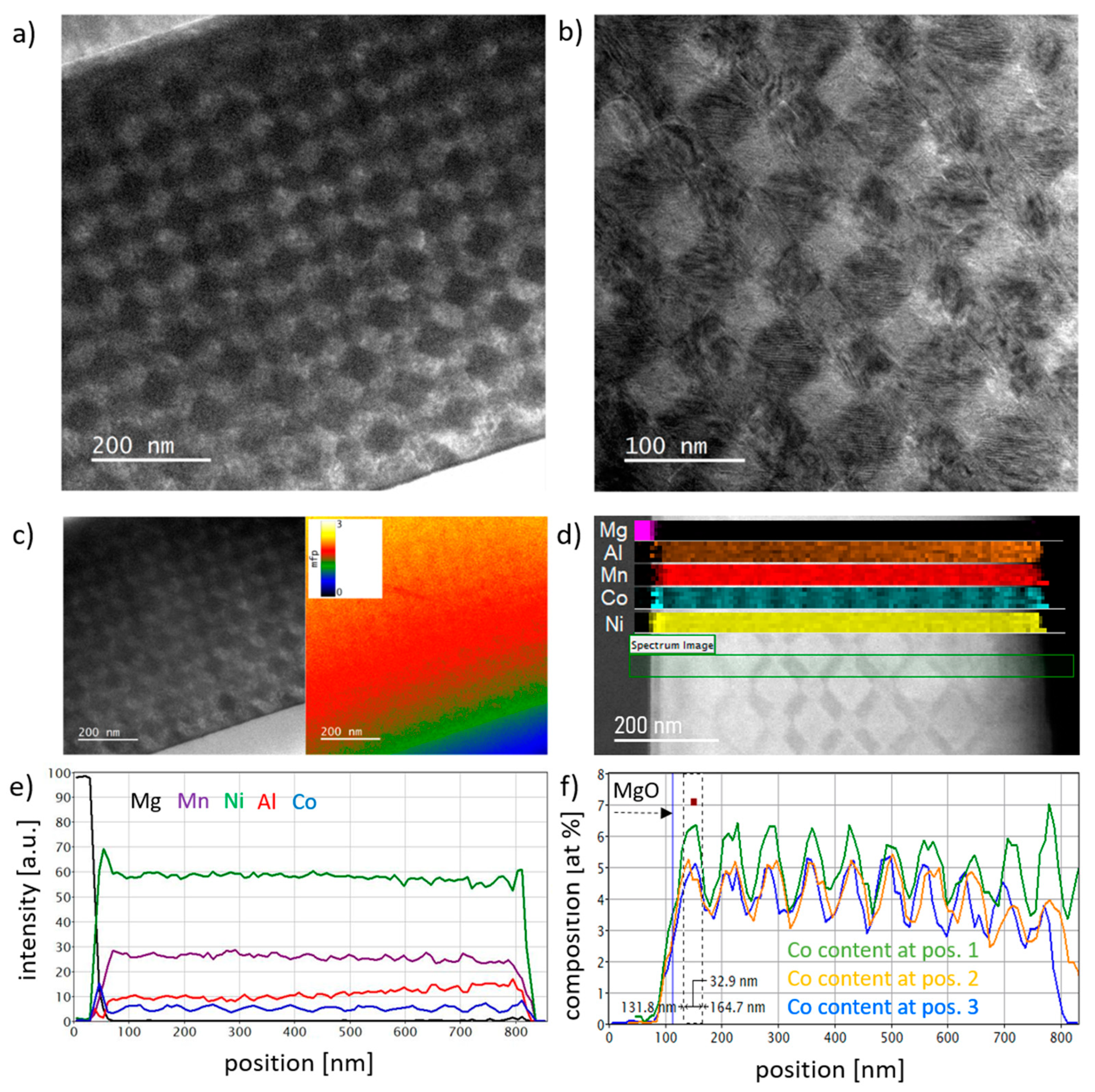
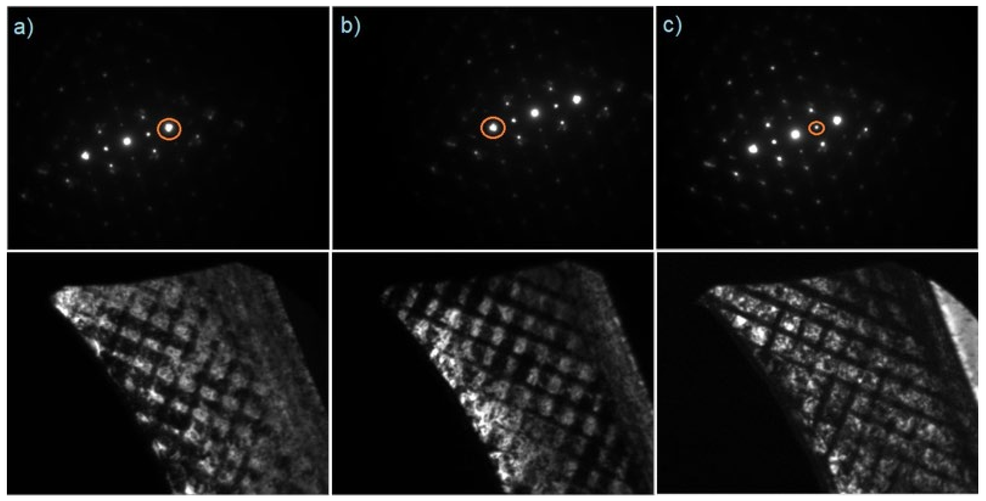
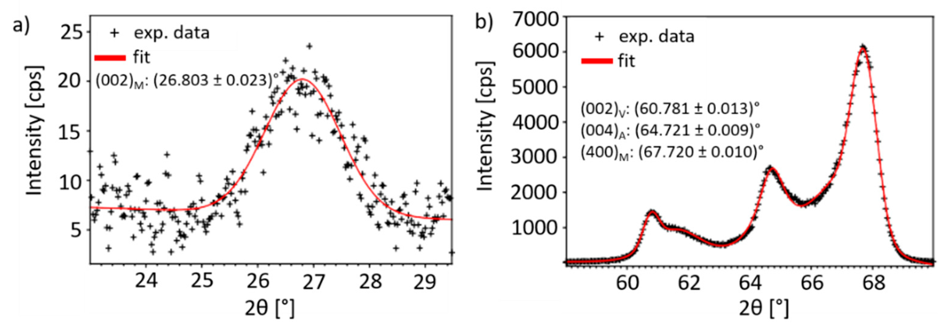
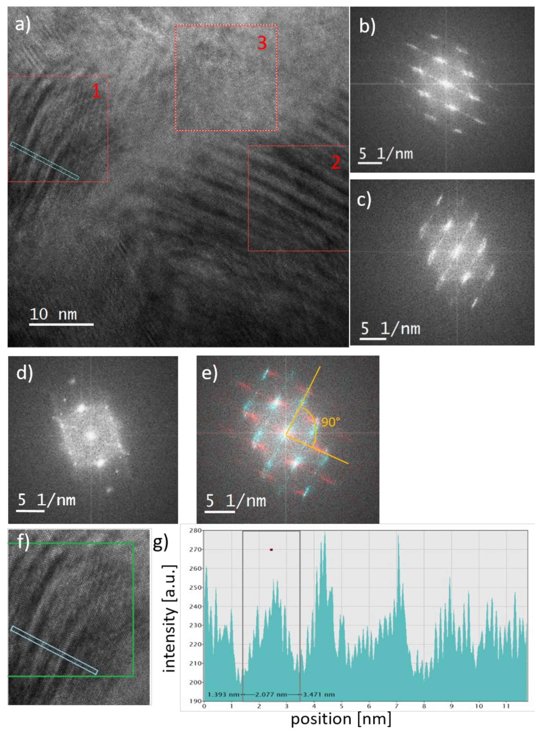
3.1. Crystalline Structure

For a better understanding of the observed nanostructure, TEM and diffraction image simulations have been carried out for the martensitic and austenitic phase of NiCoMnAl and combinations of both. As a basis for the multislice simulation a B2 structure for austenite and a tetragonal distorted B2 structure for martensite with a 14 M modulation has been assumed. In Figure 4 the results are shown, simulated at 200 kV acceleration voltage, at a temperature of 300 K and a defocus of −60 nm. The number of layers and their thickness had to be decreased due to computational effort.
It can be seen that the diffraction image of the austenite resembles its cubic structure where the martensite only allows a different class of reflexes to be excited, resulting in an unordered superposition in the center with lines of diffraction spots. Placing these two configurations of the material on top of each other leads to a pattern of austenite acting as a base with added reflexes from martensite around the excited austenite reflexes. More reflexes are visible on the austenite reflexes in the preferred scattering direction of the martensite, less in the perpendicular direction. Of course, not all of the reflexes shown in the simulation are strong enough to be visible in the TEM, depending on the specimen thickness and all contained crystal structures the electron wave has to cross. By employing FFT on the simulated diffraction pattern, possible HRTEM images can be generated (Figure 4b), which give insights in the structure. Especially, the 14M modulation of the martensite is visible in the image (Figure 4b, center). Processing the simulated diffraction pattern of martensite on top of austenite (Figure 4b, right) reveals the origin of the observed Moiré patterns in the dark checkerboard fields. The direction of the Moiré patterns gives information about the orientation of the martensite cell and the periodicity is measured to be 2.01 nm.
A first step to identify the microstructural properties of the checkerboard has been carried out by XRD analysis. A θ/2θ-scan for the (002)M peak as well as the (004)A and (400)M peaks are shown in Figure 5a,b), respectively. A linear function has been used for background subtraction and the peaks have been fitted by Pseudo-Voigt-functions. The fit of the (004)A peak yields a 2θ-angle of (64.721 ± 0.009)°, from which, according to Bragg’s equation, a lattice constant of (5.761 ± 0.008) Å for the austenite unit cell has been calculated. For the martensite (002)M peak a position of (26.803 ± 0.023)° and for the (400)M peak a position of (67.720 ± 0.010)° have been determined. Therefore, the unit cell parameters of the tetragonal cell have been calculated to be a = (5.534 ± 0.010) Å and c = (6.652 ± 0.018) Å. These values are in close agreement with lattice constants found in other studies for this alloy [30]. Here, a tetragonality factor cT = (1.202 ± 0.003) for the martensite has been determined. In order to adapt the fit for the (004)A and (400)M peak, the (002) peak from the V seed layer located at (60.781 ± 0.013)° has to be considered as well. Additionally, two more Pseudo-Voigt functions have to be introduced centered at (61.593 ± 0.186)° and (66.775 ± 0.169)° for the fit to converge. Both peaks could be caused by the 14 M-modulated superstructure occurring in this Heusler compound.
A HRTEM image of bright and darker checkerboard fields is shown in Figure 6a. The FFT analysis of different parts of the image reveal the existence of different martensite and austenite unit cells. Only the bright, rectangle regions which show no Moiré-patterns consist of a purely austenite lattice (Figure 6d). In contrast to that, each of the squared, darker regions show the presence of a martensite nucleus with different orientations, which most likely form a modulated structure. Furthermore, a superposed austenite pattern could be measured in those regions as well (compare Figure 6b,c). Most likely, the austenite is located in front of or behind the martensite nuclei, which is possible due to the large thickness of the TEM-lamella. Moreover, the observed Moiré-patterns in the darker fields are perpendicular to each other, which can be nicely seen in the overlay of both FFTs given in Figure 6e). The line profile of the Moiré pattern visible in field 1 of the HRTEM image reveals a peak-to-peak distance of 2.07 nm between the Moiré fringes (Figure 6g), which is in good agreement with the value obtained from simulation for martensite on austenite. Clearly evident from this is that neither the MIs nor the ALs are fully in the austenite or martensite state.

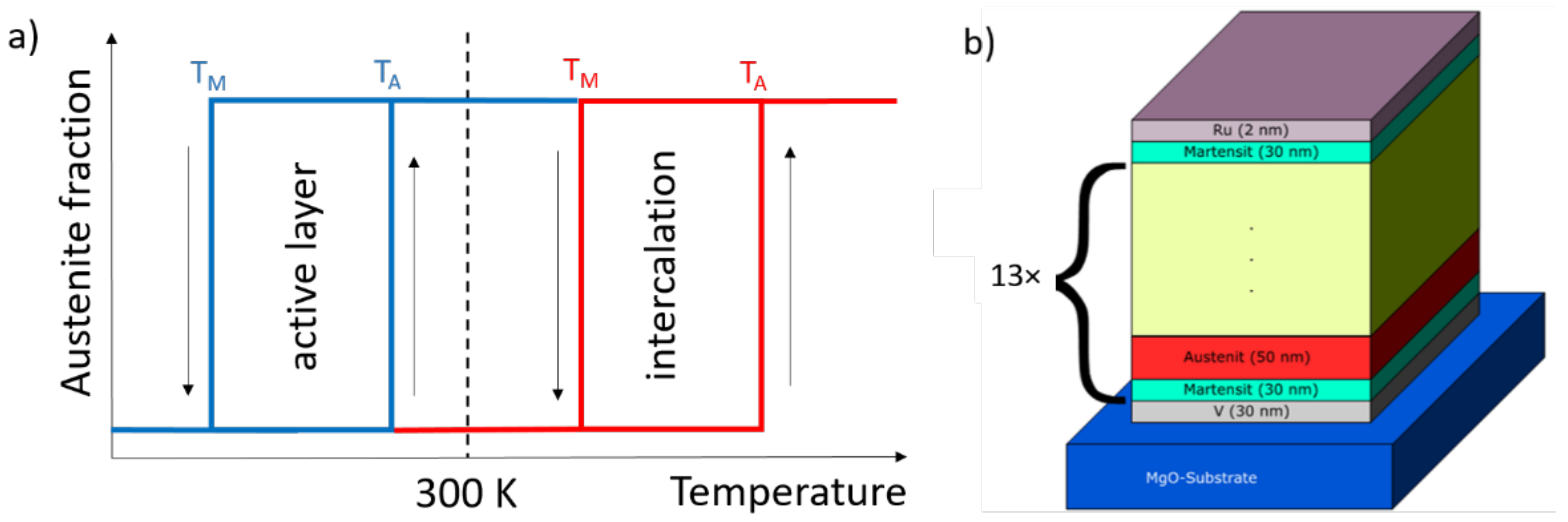
3.2. Temperature Dependence

To observe the phase transition of the checkerboard pattern temperature dependent TEM experiments have been carried out. In Figure 7a TEM images of the checkerboard system at different temperatures are shown. The change of the checkerboard structure is clearly visible. It starts to vanish at 363 K and is mostly gone at 383 K. This indicates again that the pattern originates from different crystal structures in different fields. At temperatures above 400 K the whole system is transformed into austenite, as can be seen in the FFT diffraction pattern (Figure 7b). After cooling down the specimen to room temperature the checkerboard pattern is present as before heating. In a cooling experiment the specimen has been cooled to 103 K. At this low temperature the system is transformed in the martensitic phase (Figure 7c). Here, the checkerboard pattern vanishes again and regular Moiré pattern appear. Partly, the pattern exhibits quadratic forms or are at least perpendicular to those of the next region. This is probably a preliminary stage of the checkerboard structure, where the quadratic regions become part of the checkerboard fields. In the diffraction pattern shown in Figure 7c) are two sets of rows of reflexes perpendicular to each other visible. Each set of rows shows a distance of 0.4671/nm between two parallel rows, which is in good agreement with the simulation for the diffraction pattern of the martensite phase. Thus, two martensitic grains with perpendicular orientation are present in the field of view.

3.3. Influence of the Layer Thicknesses on the Checkerboard Formation

In order to check if the observed pattern is an exception or caused by a general formation mechanism in these type of thin film systems, the sample has been reproduced and different intercalation and active layer thicknesses have been investigated. In Figure 8 TEM images of four different samples have been summarized. The details of the investigated sample systems and an explanation of the sample nomenclature are given in Table 1. In the survey image in Figure 8a of a sample with 7 martensitic intercalations (MI7-30/100) no checkerboard structure can be identified easily, but on closer inspection, rectangular regions containing Moiré-patterns can be identified (see inset). Similar to the sample with 13 MIs those regions are tilted by 45° to the sample surface. Another shared feature for both samples is the perpendicular arrangement of the Moiré-patterns of two adjacent regions. Thus, the sample might be on the verge of forming the regular arrangement of martensite nuclei. In the MI6-30/30 and MI6-30/50 samples the checkerboard arrangement is present, as can be seen in Figure 8b,c. The contrast between the rectangular regions is not as large as before, caused by the smaller thickness of both cross sections. Nevertheless, the field sizes have been determined to be about (25.3 ± 8.2) nm for the small squares, (46.8 ± 7.6) nm for the large squares and (25.3 ± 8.2) nm × (46.8 ± 7.6) nm for rectangle areas of sample MI6-30/30. For the MI6-30/50 sample, slightly larger field sizes have been measured: (38.3 ± 5.2) nm for the small squares, (53.7 ± 6.6) nm for the large squares and (38.3 ± 5.2) nm × (53.7 ± 6.6) nm for the rectangle regions. The measured values are similar to that one’s measured from the MI13-sample, pictured in Figure 2. Therefore, the sizes of the checkerboard fields seem to be almost independent from the thicknesses of the intercalation and active layers.
Whereas, in the MI6-10/30 sample no notable features of a checkerboard formation can be identified (Figure 8d), representing together with the MI7-30/100 sample the limits for the thicknesses of the MIs and the ALs for the checkerboard formation.

4. Discussion

The checkerboard pattern originates of the alternating austenite and martensite layers with the martensite acting as a seed layer. The sizes of the checkerboard fields are not adapted to the abandoned layer thicknesses. From the observations it is clear that the contrast is of crystallographic origin. It seems that the austenite partly changes its form to martensite, which grows at 45° angle in a twinned form, but is still based on an austenite unit cell stretched in one direction. In [31] an inhomogeneous elastic stray field in an austenite matrix induced by a primary martensite nucleus have been predicted employing finite-element-method calculations. This stray field can facilitate the nucleation of secondary martensite nuclei in a certain distance and orientation. For the formation of the checkerboard structure those stray fields originate from primary nuclei, which will nucleate in the martensitic intercalations, facilitate the nucleation of martensite in the active layer regions.
Based on the observation that the martensite nucleus always appears as squares in the TEM cross sections, a shape of a distorted octaeder with its faces inclined by a few degrees to the {111}MgO planes seems to be possible. Assuming that the described autonucleation process occurs in the sample, the appearance of the regular checkerboard pattern can be explained. This hypothesis is supported by the observed dependence of the visibility of the pattern on the thickness of the TEM lamella. Furthermore, the absence of the checkerboard in the sample with a 100 nm thick austenitic layer (MI7-30/100) suggests, that the regular arrangement of the nuclei is only possible, if the elastic stray fields from the top and bottom martensitic intercalations penetrate most of the active layer region. Thus, there is an upper limit to the thickness of the active layers. On the other hand, if the martensite intercalation thickness is too small nucleation of primary nuclei might not be possible. It is energetically unfavorable to form small martensitic nuclei below a critical size, because the elastic energy stored in the phase and twin boundaries exceeds the reduction by the martensitic transformation. In this case the checkerboard formation is suppressed, which might be the reason for the observed absence of the checkerboard in the sample with only 10 nm thick martensitic intercalations (MI6-10/30).
Although all obtained data confirm the presented model for the arrangement of the martensitic nuclei in this system, a clear verification is still missing. Therefore, additional 3d reconstructions from tomography measurements as well as phase field simulations of the formation process of the martensite nuclei would be desirable. Nevertheless, the observed stability and reproducibility of this extraordinary arrangement opens the door for applications. It would also be interesting to repeat this experiment with materials that do not undergo a cubic to tetragonal martensitic transformation, because an appearance of a different pattern in TEM cross sections can be expected.

Author Contributions

Transmission electron microscopy, image simulations and writing, D.R.; sample preparation, XRD and writing, A.B.; fabricating cross-section lamella for transmission electron microscopy, B.B.; writing and review, A.H.; corresponding author, supervising transmission electron microscopy and writing, I.E. All authors have read and agreed to the published version of the manuscript.

Funding

This research was funded by the DFG priority program Ferroic cooling (SPP 1599), grant number 227087704 and by the BMBF joint project DiProMag—Digitalization of a process chain for the production, characterization and prototypical application of magnetocaloric alloys, here the contribution of Bielefeld University: FKZ 13XP5 120B, with the objective of producing magnetocaloric Heusler compounds and ontology development.

Institutional Review Board Statement

Not applicable.

Informed Consent Statement

Not applicable.

Data Availability Statement

Not applicable.

Conflicts of Interest

The authors declare no conflict of interest.

References

  1. Duerig, T.; Pelton, A.; Stöckel, D. An overview of nitinol medical applications. Mater. Sci. Eng. A 1999, 273–275, 149–160. [Google Scholar] [CrossRef]
  2. Hartl, D.J.; Lagoudas, D.C. Aerospace applications of shape memory alloys. Proc. Inst. Mech. Eng. Part G J. Aerosp. Eng. 2007, 221, 535–552. [Google Scholar] [CrossRef] [Green Version]
  3. Ullakko, K.; Huang, J.K.; Kantner, C.; O’Handley, R.C.; Kokorin, V.V. Large magnetic-field-induced strains in Ni2MnGa single crystals. Appl. Phys. Lett. 1996, 69, 1966–1968. [Google Scholar] [CrossRef]
  4. Saren, A.; Smith, A.R.; Ullakko, K. Integratable magnetic shape memory micropump for high-pressure, precision microfluidic applications. Microfluid. Nanofluid. 2018, 22, 38. [Google Scholar] [CrossRef]
  5. Minorowicz, B.; Leonetti, G.; Stefanski, F.; Binetti, G.; Naso, D. Design, modelling and control of a micropositioning actuator based on magnetic shape memory alloys. Smart Mater. Struct. 2016, 25, 075005. [Google Scholar] [CrossRef]
  6. Karaman, I.; Basaran, B.; Karaca, H.E.; Karsilayan, A.I.; Chumlyakov, Y.I. Energy harvesting using martensite variant reorientation mechanism in a NiMnGa magnetic shape memory alloy. Appl. Phys. Lett. 2007, 90, 172505. [Google Scholar] [CrossRef]
  7. Schleicher, B.; Niemann, R.; Diestel, A.; Hühne, R.; Schultz, L.; Fähler, S. Epitaxial Ni-Mn-Ga-Co thin films on PMN-PT substrates for multicaloric applications. J. Appl. Phys. 2015, 118, 053906. [Google Scholar] [CrossRef]
  8. Sarawate, N.; Dapino, M. Experimental characterization of the sensor effect in ferromagnetic shape memory ni–mn–ga. Appl. Phys. Lett. 2006, 88, 121923. [Google Scholar] [CrossRef] [Green Version]
  9. Kumar, P.K.; Lagoudas, D.C. Introduction to Shape Memory Alloys. In Shape Memory Alloys; Springer: Boston, MA, USA, 2008; pp. 1–51. [Google Scholar]
  10. Liu, J.; Gottschall, T.; Skokov, K.P.; Moore, J.D.; Gutfleisch, O. Giant magnetocaloric effect driven by structural transitions. Nat. Mat. 2012, 11, 620–626. [Google Scholar] [CrossRef]
  11. Neibecker, P.; Gruner, M.E.; Xu, X.; Kainuma, R.; Petry, W.; Pentcheva, R.; Leitner, M. Ordering tendencies and electronic properties in quaternary Heusler derivatives. Phys. Rev. B 2017, 96, 165131. [Google Scholar] [CrossRef] [Green Version]
  12. Xu, X.; Ito, W.; Tokunaga, M.; Kihara, T.; Oka, K.; Umetsu, R.Y.; Kanomata, T.; Kainuma, R. The Thermal Transformation Arrest Phenomenon in NiCoMnAl Heusler Alloys. Metals 2013, 3, 298–311. [Google Scholar] [CrossRef] [Green Version]
  13. Weise, B.; Dutta, B.; Teichert, N.; Hütten, A.; Hickel, T.; Waske, A. Role of disorder when upscaling magnetocaloric Ni-Co-Mn-Al heusler alloys from thin films to ribbons. Sci. Rep. 2018, 8, 9147. [Google Scholar] [CrossRef]
  14. Diestel, A.; Chekhonin, P.; Niemann, R.; Skrotzki, W.; Nielsch, K.; Fähler, S. Reducing thermal hysteresis in epitaxial Ni-Mn-Ga-Co films by transformation cycling. Phys. Status Solidi B 2018, 255, 1700330. [Google Scholar] [CrossRef]
  15. Scheibel, F.; Gottschall, T.; Taubel, A.; Fries, M.; Skokov, K.P.; Terwey, A.; Keune, W.; Ollefs, K.; Wende, H.; Farle, M.; et al. Hysteresis design of magnetocaloric materials-from basic mechanisms to applications. Energy Technol. 2018, 6, 1397–1428. [Google Scholar] [CrossRef] [Green Version]
  16. Taubel, A.; Gottschall, T.; Fries, M.; Riegg, S.; Soon, C.; Skokov, K.P.; Gutfleisch, O.A. Comparative Study on the Magnetocaloric Properties of Ni-Mn-X(-Co) Heusler Alloys. Phys. Status Solidi B 2017, 255, 1700331. [Google Scholar] [CrossRef]
  17. Devi, P.; Salazar, M.C.; Caron, L.; Singh, S.; Nicklas, M.; Felser, C. Effect of chemical and hydrostatic pressure on the coupled magnetostructural transition of Ni-Mn-In Heusler alloys. Phys. Rev. Mat. 2019, 3, 122401. [Google Scholar] [CrossRef] [Green Version]
  18. Gottschall, T.; Stern-Taulats, E.; Mañosa, L.; Planes, A.; Konstantin, P.S.; Gutfleisch, O. Reversibility of minor hysteresis loops in magnetocaloric Heusler alloys. Appl. Phys. Lett. 2017, 110, 223904. [Google Scholar] [CrossRef]
  19. Becker, A.; Ramermann, D.; Ennen, I.; Büker, B.; Matalla-Wagner, T.; Gottschalk, M.; Hütten, A. The influence of Martensitic Intercalations in Magnetic Shape Memory NiCoMnAl Multilayered Films. Entropy 2021, 23, 462. [Google Scholar] [CrossRef]
  20. Petch, N.J. The cleavage strength of polycrystals. J. Iron Steel Inst. 1953, 174, 25–31. [Google Scholar]
  21. Donelan, P. Modelling microstructural and mechanical properties of ferritic ductile cast iron. Mater. Sci. Technol. 2000, 16, 261–269. [Google Scholar] [CrossRef]
  22. Osório, W.R.; Santos, C.A.; Quaresma, J.M.V.; Garcia, A. Mechanical properties as a function of thermal parameters and microstructure for Zn-Al castings. J. Mater. Proc. Technol. 2003, 143, 703–709. [Google Scholar] [CrossRef]
  23. Lloyd, D.J.; Court, S. Influence of grain size on tensile properties of Al-Mg alloys. Mater. Sci. Technol. 2003, 19, 1349–1354. [Google Scholar] [CrossRef]
  24. Osório, W.R.; Cheung, N.; Spinelli, J.E.; Goulart, P.R.; Garcia, A. The effects of a eutectic modifier on microstructure and surface corrosion behavior of Al-Si hypoeutectic alloys. J. Solid State Electrochem. 2007, 11, 1421–1427. [Google Scholar] [CrossRef]
  25. Bonatti, R.S.; Meyer, Y.A.; Bortolozo, A.D.; Costa, D.; Osório, W.R. Morphology and size effects on densification and mechanical behavior of sintered powders from Al-Si and Al-Cu casting alloys. J. Alloys Compd. 2019, 786, 717–732. [Google Scholar] [CrossRef]
  26. Meyer, Y.A.; Bonatti, R.S.; Costa, D.; Bortolozo, A.D.; Osório, W.R. Compaction pressure and Si content effects on compressive strengths of Al-Si/Cu alloy composites. Mater Sci. Eng. A 2020, 770, 138547. [Google Scholar] [CrossRef]
  27. Wodniok, M.; Teichert, N.; Helmich, L.; Hütten, A. How to enable bulk-like martensitic transformation in epitaxial films. AIP Adv. 2017, 7, 056428. [Google Scholar] [CrossRef] [Green Version]
  28. Koch, C. Determination of Core Structure Periodicity and Point Defect Density along Dislocations. Ph.D. Thesis, Arizona State University, Tempe, AZ, USA, 2002. [Google Scholar]
  29. Williams, D.B.; Carter, C.B. Transmission Electron Microscopy—A Textbook for Materials Science; Plenum Press: New York, NY, USA, 1994; pp. 444–448. [Google Scholar]
  30. Teichert, N.; Kucza, D.; Yildirim, O.; Yuzuak, E.; Dincer, I.; Behler, A.; Weise, B.; Helmich, L.; Boehnke, A.; Klimova, S.; et al. Structure and giant inverse magnetocaloric effect of epitaxial Ni-Co-Mn-Al films. Phys. Rev. B 2015, 91, 184405. [Google Scholar] [CrossRef] [Green Version]
  31. Niemann, R.I. Nukleation und Wachstum des Adaptiven Martensits in Epitaktischen Schichten der Fromgedächtnislegierung Ni-Mn-Ga. Ph.D. Thesis, Technische Universität Dresden, Dresden, Germany, 2015. [Google Scholar]
Figure 1. (a) The chosen compositions result in completely separated thermal hystereses for the active (blue) and intercalation layers (red). (b) Illustration of the sample system with 13 martensitic intercalations.
Applsci 12 01748 g001
Figure 2. TEM images of a cross section show a 3D-checkerboard structure (a,b). (c) EFTEM thickness map. (d) STEM dark field image of the checkerboard sample with the overlaid EDX elemental mappings. The scanned area is marked by the green rectangle. (e) Corresponding line profiles of the elemental compositions. (f) EDX line profiles of the Co content extracted from EDX mappings measured on three different regions across the whole lamella. The layer modulation in the Co content is clearly visible.
Applsci 12 01748 g002
Figure 3. Selected area diffraction pattern (upper row) and corresponding dark field images (lower row) of the same checkerboard area. The diffraction spots used for the respective DF images are marked by the orange circles.
Applsci 12 01748 g003
Figure 4. (a) Multislice simulation of diffraction images for the pure austenitic (left) and martensitic (centre) phase of NiCoMnAl and 3 nm martensite on top of 3 nm austenite (right). (b) Corresponding TEM images created via FFT of the diffraction pattern. The images are still depending on parameters such as defocus and camera length.
Applsci 12 01748 g004
Figure 5. θ/2θ-scan measured at room temperature for the (a) (002)M peak and (b) (004)A and (400)M peaks and the correspondent fits.
Applsci 12 01748 g005
Figure 6. (a) HRTEM image of a section of the checkerboard. The red boxes mark the fields from that FFTs have been obtained. The FFT of box 1 is given in (b) of box 2 is shown in (c) and (d) corresponds to box 3. (e) Overlay of the FFTs b) and (c) illustrating the perpendicular orientation of adjacent martensite nuclei. (f) Enlarged image of box 1 indicating the region where a line profile across the Moiré pattern has been obtained and (g) the resulting line profile with a measured distance of 2.07 nm between the Moiré fringes.
Applsci 12 01748 g006
Figure 7. Temperature evolution of the checkerboard sample: (a) TEM images acquired between 323 K to 403K and their corresponding FFT diffraction pattern (b). All FFTs have been contrast adjusted. (c) TEM image of the specimen recorded at 103 K (enhanced in contrast to make the Moiré pattern more visible) and corresponding SAED pattern.
Applsci 12 01748 g007
Figure 8. (a) A checkerboard pattern is not clearly visible in the survey TEM image of the MI7-30/100 sample. The inset contains a close up. Moiré patterns, which are tilted by 90° to each other, are slightly visible. TEM images of the MI6-30/30 sample (b) and MI6-30/50 sample (c) showing the checkerboard structure. (d) For the MI6-10/30 sample no checkerboard pattern can be detected.
Applsci 12 01748 g008
Table 1. Overview about the details of the investigated sample systems. The sample names contain the number of the martensitic intercalation (MI) and the nominal thicknesses of the layers in nm for MIs and active layers (AL).
Sample NameMI NumberMI Thickness [nm]AL NumberAL Thickness [nm]
MI7-30/1007306100
MI6-30/30630530
MI6-30/50630550
MI6-10/30610530
Publisher’s Note: MDPI stays neutral with regard to jurisdictional claims in published maps and institutional affiliations.

