Article

Enhancement-Mode Heterojunction Vertical β-Ga2O3 MOSFET with a P-Type Oxide Current-Blocking Layer

1
Wide Bandgap Semiconductor Technology Disciplines State Key Laboratory, Shaanxi Joint Key Laboratory of Graphene, School of Microelectronics, Xidian University, Xi’an 710071, China
2
Qinghai Huanghe Hydropower Development Co., Ltd., Xining 810008, China
*
Author to whom correspondence should be addressed.
Submission received: 29 December 2021 / Revised: 22 January 2022 / Accepted: 26 January 2022 / Published: 8 February 2022
(This article belongs to the Special Issue Advanced Compound Semiconductor)

Abstract

:
The vertical heterojunction Ga2O3 MOSFET (Metal-Oxide-Semiconductor Field-Effect Transistor) with the p-type oxide as the current-blocking layer (CBL) is investigated for the first time using SILVACO simulation software. The results show that the threshold voltage of the device is easily positive, which means that the device works in the enhancement mode. By adjusting the doping concentration (from 2 × 1017 cm−3 to 2 × 1018 cm−3) and thickness (from 0.4 um to 2 um) of p-SnO CBL, the threshold voltage is around from 2.4 V to 2.8 V and the breakdown voltage of the device can be increased from 361 V to 518 V. Compared with the original homojunction Ga2O3 vertical MOSFET with CBL, the p-SnO CBL can greatly improve the performance of the device. Other p-type oxides are also investigated as the CBL and show promising performances. This work has a certain guiding significance for the design of a vertical enhanced current-blocking layer MOSFET device and for the development of a Ga2O3 heterojunction power device.

1. Introduction

Due to the ultra-wide bandgap of about 4.5–4.9 eV [1,2,3], β-Ga2O3 has a high critical field strength of 5–9 MV/cm [4]. These characteristics make Ga2O3 a strong competitor for the next generation of power electronic devices. Although Ga2O3 materials have such attractive advantages, due to its low thermal conductivity and various p-type doping problems (such as large effective hole mass [5,6,7,8] and large activation energy of traditional acceptors [3,9,10]), the performance of β-Ga2O3 devices is still extremely inferior to those of GaN and SiC. To solve these problems, novel device structures, especially heterostructures that have the greatest potential to make use of Ga2O3 materials, are urgently required.
In high-voltage applications, a vertical device can withstand a higher voltage and has a much smaller device area compared with a transverse device, so a vertical device has more advantages. At present, some vertical Ga2O3 MOSFETs have been reported, including MOSFETs with Mg-ion implantation and N-ion implantation current-blocking layers (CBLs) [11,12], and single-fin or multi-fin gate vertical FinFETs [13,14]. Compared with a Ga2O3 vertical FinFET, the fabrication process of vertical Ga2O3 MOSFETs with CBL is relatively simple and currently has more potential to be realized. Although the reported vertical Ga2O3 MOSFET with CBL can work in the enhanced mode, its breakdown voltage is still temporarily at a low level, which is due to the negative effect of the lack of p-type doping and the corresponding PN junction in Ga2O3, resulting in a low device performance.
In recent years, p-type metal oxides (SnO, NiO, etc.) have become a hot topic because of their high hole concentration. Due to the Ga2O3 p-type doping problem, the p-type metal oxide provides an alternative way to form the heterojunction for Ga2O3 device application. At present, Ga2O3 heterojunction devices have been reported [15,16,17,18,19,20,21] but mainly used in the heterojunction diode. Additionally, none of vertical heterojunction Ga2O3 MOSFETs has been studied in detail.
In this paper, the vertical heterojunction MOSFET with p-type SnO and other metal oxides as CBLs are studied for the first time using SILVACO software. Additionally, the simulation calculation in SILVACO is mainly based on Poisson’s equation, the drift-diffusion transport equation, the Fermi distribution equation, and the impact ionization equation. Due to the hybrid orbital of p-SnO forming the effective hole transport path, it has relatively high hole mobility [22], which can be prepared by sputtering, PLD (Pulsed Laser Deposition), and electron beam technology [21,22,23,24]. The simulation result shows that the breakdown voltage of a vertical heterojunction MOSFET with a p-SnO CBL can be increased from 361 V to 518 V by adjusting the p-type doping concentration (from 2 × 1017 cm−3 to 2 × 1018 cm−3), and the threshold voltage can be adjusted in a small range (2.4–2.8 V). Other p-type oxides are also investigated as the CBL and show promising performances. This work has a certain guiding significance for the fabrication of vertical heterojunction MOSFET with CBL and for the development of Ga2O3-based heterojunction power device.

2. Methods

In order to improve the accuracy of the model and the simulation results, we first carried out the model calibration using the reported results [25]. To save on calculation time, half of the device was established for calculation based on the symmetry of the structure. The device structure and some parameters are shown in Figure 1a. Table 1 also shows the geometrical parameters of the simulated device. As shown in Figure 1a, Lap was 10 um. To make the CBL form a certain high-resistance region, the region was set as p-type Ga2O3 region in the simulation, which was a virtual pn homojunction and was adopted in other reports [26]. The simulation result is shown in Figure 1b,c. When the gate voltage was 0 V, the breakdown voltage was 263 V (when the current exceeded 1 A/cm2, the corresponding voltage was the breakdown voltage); when the gate voltage was 6 V and the drain voltage was 20 V, the current density was 0.028 kA/cm2. In all of the above results, the output and transfer characteristics curves and breakdown voltage of the simulation model are consistent with those reported in another study [25], which verifies the accuracy and feasibility of the model and simulation result. Based on the verified model, p-SnO and other p-type metal oxides as CBLs were included. How the thickness of p-SnO CBL and its doping concentration affect the breakdown voltage and Vth of the device were mainly studied.

3. Results

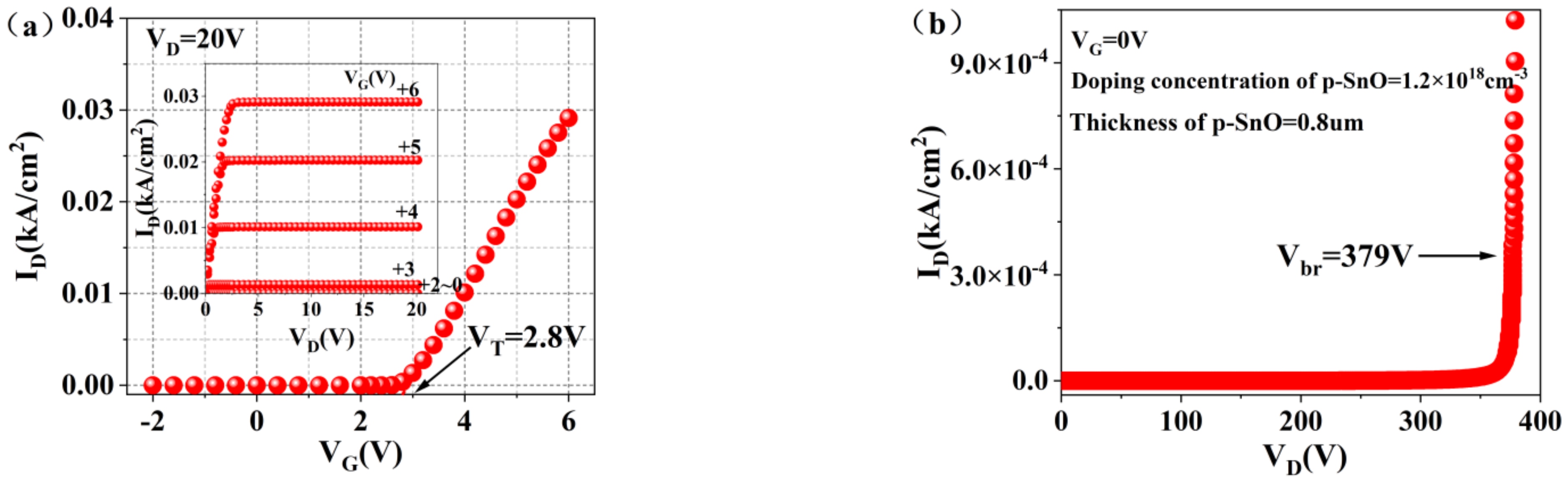
3.1. Basic Characteristics

p-SnO was used as the CBL while all other factors remain unchanged. The output curve of the device is shown in Figure 2a, when the gate voltage was 0–6 v (the step size was 1 V) and the saturated leakage current density of the device was 0.029 kA/cm2 at 6 V. Additionally, the Vth of the device was positive, which was 2.8 V. This shows that, after replacing the CBL material with p-SnO, the threshold voltage of the device is less affected and the device can still be in the enhanced mode. Here, the p-type doping concentration of CBL is equivalent to the original one.
As seen in Figure 2b, the breakdown voltage of the device reached 379 V. Compared with the original device, the breakdown voltage of the heterojunction device increased by 44% when other parameters (such as the doping concentration and thickness of each part) remained unchanged, except for the change in material.
To better analyze the change in threshold voltage after replacing the CBL material, the transverse and longitudinal conduction band diagrams of the device were extracted from the simulation results. The transverse extraction range is shown by the red solid line in Figure 1a (in the channel near the bottom of Al2O3), and the longitudinal extraction range is shown by the red dotted line in Figure 1a. The extraction results are shown in Figure 3a,b. It can be seen from Figure 3a that, when SnO is used as the CBL material, the average conduction band height in n-Ga2O3 channel layer is lower than that of Ga2O3 as the CBL. Through ouor study and analysis of the electron affinity and band gap width of SnO and Ga2O3, it was found that, because the electron affinity and band gap width of SnO are less than Ga2O3, a II-type heterojunction formed at the interface between the p-SnO CBL and the n-Ga2O3 channel layer. When the heterojunction formed, a “spike” and “notch” formed at the interface of SnO and Ga2O3 materials with different band gap widths, resulting in a sudden change in the energy band at the interface. It can be seen in the heterojunction at the circle in Figure 3a. After the heterojunction formed, the conduction band energy in the channel of SnO heterojunction MOSFET became lower than that in Ga2O3 MOSFET due to the sudden change in energy band at the interface, and finally, the threshold voltage of SnO heterojunction MOSFET became slightly lower than that of Ga2O3 MOSFET. This can also be seen from Figure 3b, which shows the conduction band diagram of the channel at 0 V gate voltage and the threshold voltage. The channel barrier of SnO heterojuncion MOSFET in the cut-off state was lower than that of the original device, so when the gate voltage increased, the gate voltage required to reach the channel conduction condition was relatively reduced.

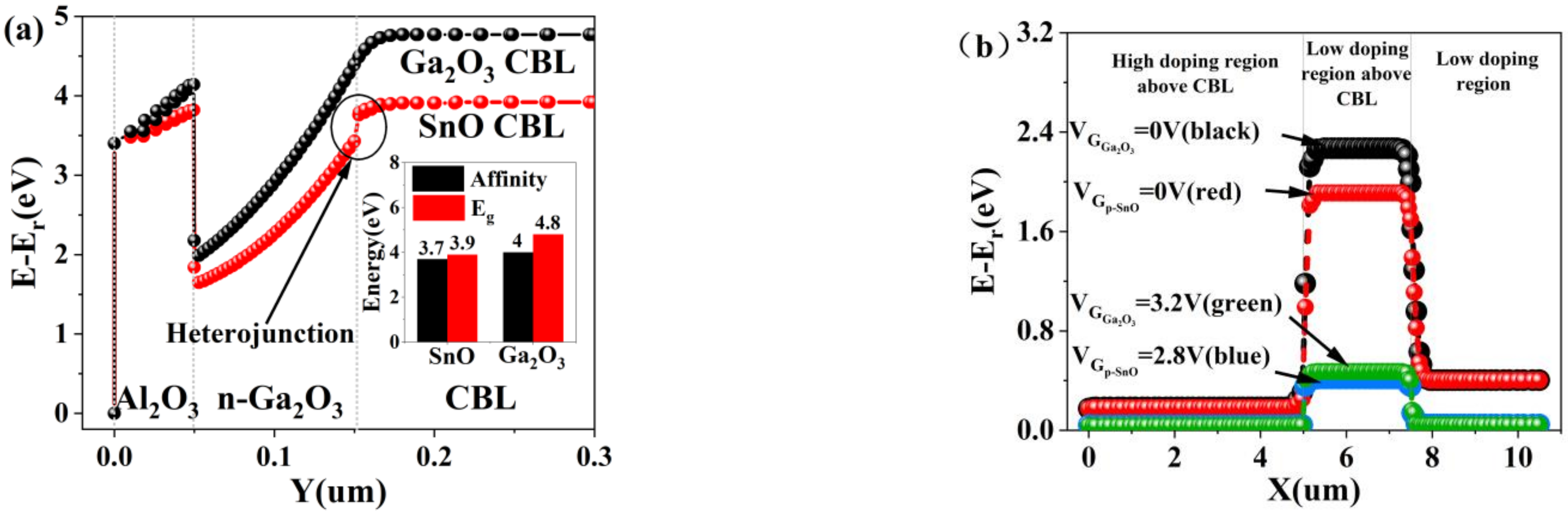
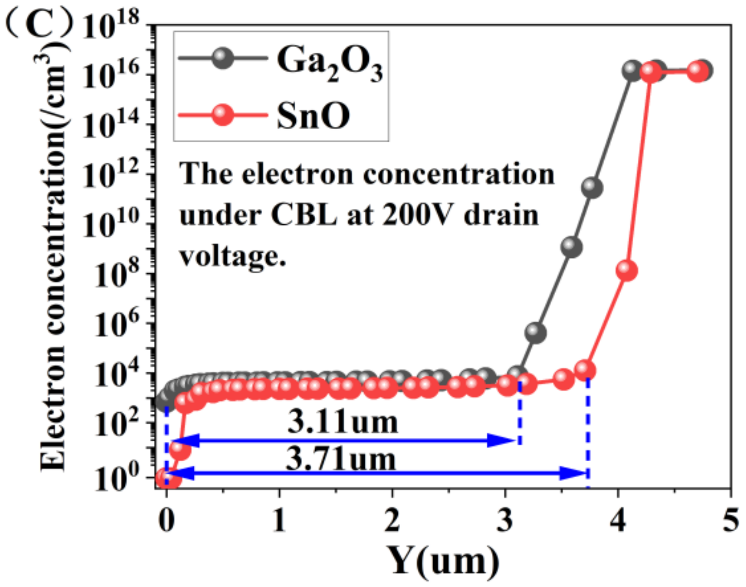
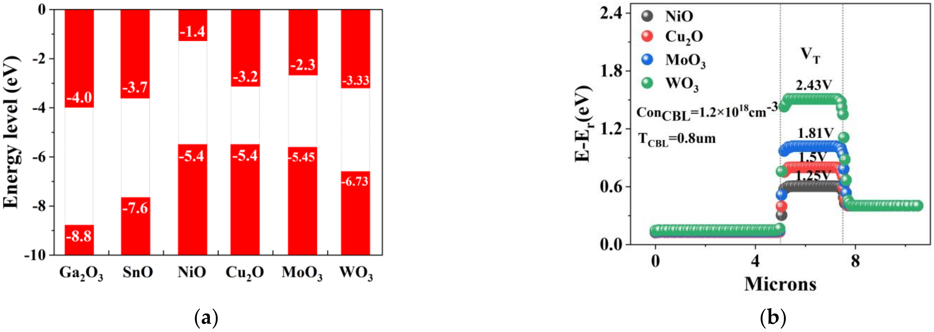
3.2. Analysis of Energy Band Structure and Characteristics

The increase in breakdown voltage mainly comes from the influence of different materials on the thickness of depletion layer. Since the voltage at the time of breakdown is much greater than the built-in potential of the heterojunction, the depletion layer width of the heterojunction device is given by the following Formula (1):
W h e t e r o j u n c t i o n = 2 ε 1 ε 2 N A 1 + N D 2 2 V q N A 1 N D 2 ε 1 N A 1 + ε 2 N D 2
Among them, ε 1 and ε 2 are the dielectric constants of SnO and Ga2O3, respectively; N A 1 and N D 2 are the p-type doping concentration of SnO and n-type doping concentration of Ga2O3, respectively; V is the applied voltage; and q is the electron charge.
Similarly, when the applied voltage is much greater than the built-in potential, the Formula (2) for the depletion region width of the PN junction of the same material is given:
W p n = 2 ε 2 V N A 1 + N D 2 q N A 1 N D 2
Among them, ε 2 is the dielectric constant of Ga2O3; N A 1 and N D 2 are the p-type and n-type doping concentrations of Ga2O3; V is the applied voltage; and q is the electron charge.
To better compare the effects of homogeneous junction and heterojunction on the width of depletion layer, the following comparison Formula (3) is given and simplified:
W h e t e r o j u n c t i o n W p n = N A 1 + N D 2 ε 2 ε 1 N A 1 + N D 2
As can be seen from the above formula, ε 2 < ε 1 , that is, the dielectric constant of CBL material is greater than that of Ga2O3 material. Under the same applied voltage, the depletion region formed by heterojunction is wider than that of homogeneous junction. A wider depletion layer means being better able to withstand higher voltages and having a greater breakdown voltage of the device. This can be seen from the depletion layer width of the simulation results. As shown in Figure 3c, the dielectric constant of SnO is greater than that of Ga2O3, and the thickness of the depletion layer generated by its heterojunction is thicker than that of the original device. Under the same breakdown field strength, the greater the depletion thickness, the greater the voltage applied to the depletion layer and the higher the breakdown voltage of the device.

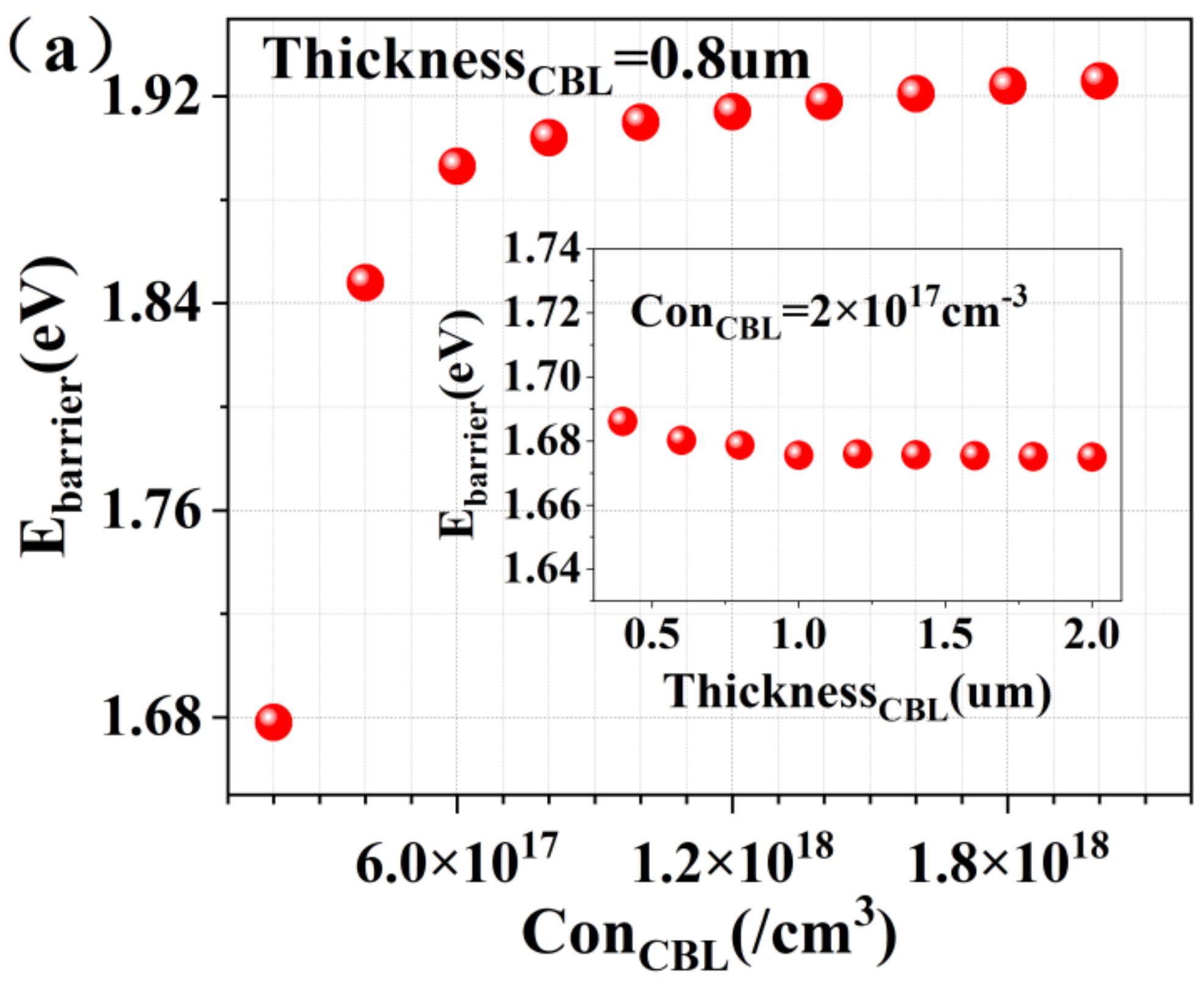
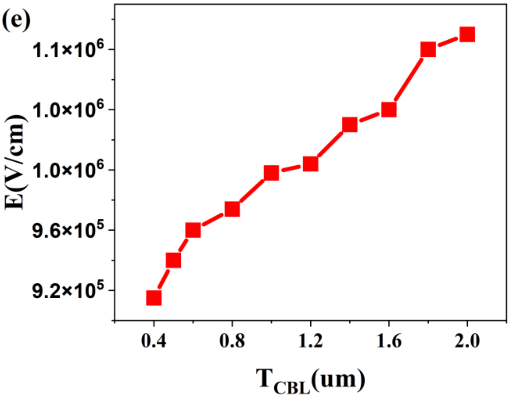
3.3. Influence of Doping Concentration and Thickness of p-SnO CBL

In this section, the effects of p-type doping concentration and thickness of p-SnO CBL on the basic characteristics of device are systematically studied.
As shown in Figure 4a,b, when the thickness of p-SnO CBL was set to 0.8 um and the p-type doping concentration increased from 2 × 1017 cm−3 to 2 × 1018 cm−3, the breakdown voltage of Ga2O3 MOSFET with a p-SnO CBL can be in the range from 361 V (corresponding to 2 × 1018 cm−3 doping concentration) to 518 V (corresponding to 2 × 1017 cm−3 doping concentration), and the threshold voltage was in the range of 2.4–2.8 V. As shown in Figure 4c, the breakdown voltage of the vertical MOSFET with p-SnO CBL has a peak value. When the thickness of CBL was about 0.8 um, the breakdown voltage of the device reached a peak value of 518 V. When the thickness of CBL increased or decreased, the breakdown voltage decreased correspondingly, and the threshold voltage range of the device was small, which was 2.4–2.8 V. By adjusting the p-type doping concentration and thickness of p-SnO CBL, the breakdown voltage of the device can be greatly increased and the threshold voltage of the device can be adjusted in a small range to improve the performance of the device, which is conducive to the preparation of power devices.
To better understand the physical mechanism of p-type doping concentration and thickness of p-SnO CBL on the device, the energy band diagrams of CBL with different p-type doping concentration and thickness are extracted in Figure 5a. As shown in Figure 5a, the higher the p-type doping concentration of CBL, the higher the potential barrier in the channel region. To achieve the low barrier conduction state, a higher gate voltage is required so that the threshold voltage of the device is increased. In Figure 5a, the thickness of p-SnO CBL hardly affects the height of channel barrier, so the threshold voltage of the device hardly changes. As for the breakdown voltage, it can be seen from Figure 5b that the lower the p-type doping concentration of CBL, the thicker the depletion layer thickness of the drift layer of the device, causing an increase in the breakdown voltage. To see the relationship between CBL thickness and depletion layer more intuitively, the parameter was directly extracted from the simulation results and a curve was drawn, shown in Figure 5c. With the increase in CBL thickness, the effective depletion layer thickness increased and the breakdown voltage increased. Until the CBL thickness reached 0.8 um, the effective depletion layer thickness decreased and the breakdown voltage decreased. Additionally, that is consistent with the previous trend of breakdown voltage.
As seen from the above Formula (1), when the doping concentration and material remained unchanged, the thickness of the depletion layer mainly depended on the applied voltage. The CBL was thin and the device broke down, as seen from the left side of Figure 5d. At this time, there was a certain concentration of electrons in the CBL, indicating that part of the current flowed directly from the CBL. Additionally, the CBL lost the function of blocking the current, so the breakdown voltage of the device decreased and the thickness of the depletion layer decreased similarly. When the thickness of CBL increased, as shown on the right side of Figure 5d, the current in the CBL layer gradually decreased to 0. At this time, the breakdown voltage increased and the thickness of the depletion layer showed an upward trend. As can be seen from Figure 5e, with the increase in the thickness of the current barrier layer, under the same applied voltage (VDS = 150 V), the edge peak electric field intensity of CBL also increased and the location of device breakdown was also at the edge of the lower right corner of CBL because the location was just at the sharp corner of CBL. It is well known that the electric field intensity at the sharp corner is the largest, the increase in edge peak electric field leads to the corresponding decrease in breakdown voltage, and then the thickness of depletion layer also decreases. Therefore, the reason for the thickest depletion layer formed by 0.8 um CBL is mainly that, when the thickness is less than 0.8 um, the effect of CBL plays a decisive role in the breakdown voltage and, when the thickness is more than 0.8 um, the peak electric field intensity at the edge of CBL plays a decisive role in the breakdown voltage.

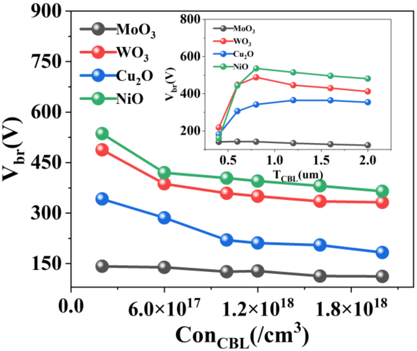
3.4. Other p-Type Metal Oxide CBL Ga2O3 Heterojunction MOSFETs

For a comparison with other p-type metal oxides, NiO, Cu2O, WO3, and MoO3 were selected as the CBL of a Ga2O3 heterojunction MOSFET, and the relevant material simulation parameters were from References [27,28,29,30]. Figure 6 shows the channel conduction band of heterojunction device with different p-type metal oxide CBLs and its threshold voltage. It can be seen from the figure that, under different materials, the barrier height is different in the channel region, resulting in different threshold voltages. The trend relationship between the barrier height and the threshold voltage is consistent, as described above.
As can be seen from Figure 7, by adjusting the doping concentration and thickness of the CBL, the other p-type metal oxides can also be used as the CBL to control the overall breakdown voltage of the device in a large range. It is worth noting that, except for Cu2O and MoO3 as the CBL, compared with Ga2O3 CBL, other p-type metal oxides can improve the breakdown voltage to a certain extent at the same doping and thickness level, which is consistent with the dielectric constant-related results described above.

4. Conclusions

By adjusting the doping concentration and thickness of the p-SnO CBL, the threshold voltage of the device can be adjusted in a small range of 2.4–2.8 V, and the breakdown voltage of the device is greater than 361 V, up to 518 V. Compared with the original vertical MOSFET with Ga2O3 CBL, using heterojunction p-type metal oxide as the CBL can greatly improve the performance of the device. Other p-type oxides such as NiO, Cu2O, WO3, and MoO3 are also investigated as the CBL and show promising performances. This work has a certain guiding significance for the design of a vertical enhanced MOSFET with CBL and for the development of a Ga2O3-based heterojunction power device.

Author Contributions

Conceptualization, C.Z.; methodology, Y.H. (Yuwen Huang); validation, X.X., Z.Z. and P.D.; formal analysis, Z.L., D.C., W.Z. and S.Z.; investigation, Q.F. and J.Z.; writing—original draft preparation, Y.H. (Yuwen Huang); writing—review and editing, C.Z.; project administration, Y.H. (Yue Hao); funding acquisition, C.Z. and Y.H. (Yue Hao). All authors have read and agreed to the published version of the manuscript.

Funding

This work was partly financially supported by the Fundamental Research Funds for the National 111 Center (Grant No. B12026), by the National Key R&D Program of China under grant 2018YFB0406500, by the National Natural Science Foundation of China under Grant 61874083, and by the Natural Science Basic Research Program of Shaanxi under Program No. 2021JC-24.

Institutional Review Board Statement

Not applicable.

Informed Consent Statement

Not applicable.

Data Availability Statement

The data presented in this study are available on request from the corresponding author.

Conflicts of Interest

The authors declare no conflict of interest.

References

  1. Onuma, T.; Saito, S.; Sasaki, K.; Masui, T.; Yamaguchi, T.; Honda, T.; Higashiwaki, M. Valence band ordering in β-Ga2O3 studied by polarized transmittance and reflectance spectroscopy. Jpn. J. Appl. Phys. 2015, 54, 112601. [Google Scholar] [CrossRef]
  2. Higashiwaki, M.; Jessen, G.H. Guest Editorial: The dawn of gallium oxide microelectronics. Appl. Phys. Lett. 2018, 112, 060401. [Google Scholar] [CrossRef] [Green Version]
  3. He, H.; Orlando, R.; Blanco, M.A.; Pandey, R.; Amzallag, E.; Baraille, I.; Rérat, M. First-principles study of the structural, electronic, and optical properties of Ga2O3 in its monoclinic and hexagonal phases. Phys. Rev. B 2006, 74, 195123. [Google Scholar] [CrossRef] [Green Version]
  4. Hudgins, J.L.; Simin, G.S.; Santi, E.; Khan, M.A. An assessment of wide bandgap semiconductors for power devices. IEEE Trans. Power Electron. 2003, 18, 907. [Google Scholar] [CrossRef] [Green Version]
  5. Kyrtsos, A.; Matsubara, M.; Bellotti, E. On the feasibility of p-type Ga2O3. Appl. Phys. Lett. 2018, 112, 032108. [Google Scholar] [CrossRef]
  6. Lyons, J.L. A survey of acceptor dopants for β-Ga2O3. Semicond. Sci. Technol. 2018, 33, 05LT02. [Google Scholar] [CrossRef]
  7. Peelaers, H.; Lyons, J.L.; Varley, J.B.; van de Walle, C.G. Deep acceptors and their diffusion in Ga2O3. APL Mater. 2019, 7, 022519. [Google Scholar] [CrossRef] [Green Version]
  8. Tomoya, G.; Kumagai, Y.; Oba, F. First-principles study of self-trapped holes and acceptor impurities in Ga2O3 polymorphs. Phys. Rev. Mater. 2019, 3, 044603. [Google Scholar]
  9. Yamaguchi, K. First principles study on electronic structure of beta- Ga2O3. Solid State Commun. 2004, 131, 12. [Google Scholar] [CrossRef]
  10. Hartwin, P.; de Walle, V.; Chris, G. Brillouin zone and band structure of β-Ga2O3. Phys. Status Solidi B Basic Res. 2015, 252, 4. [Google Scholar]
  11. Shigenobu, Y.; Hisashi, M.; Akito, K.; Ken, G.; Yoshinao, K.; Masataka, H.; Yoji, M.; Hoi, W.M. All-ion-implanted planar-gate current aperture vertical Ga2O3 MOSFETs with Mg-doped blocking layer. Appl. Phys. Express 2018, 11, 064102. [Google Scholar]
  12. Wong, M.H.; Goto, K.; Murakami, H.; Kumagai, Y.; Higashiwaki, M. Current Aperture Vertical β-Ga2O3 MOSFETs Fabricated by N- and Si-Ion Implantation Doping. Electron. Device Lett. 2018, 40, 431. [Google Scholar] [CrossRef]
  13. Hu, Z.; Nomoto, K.; Li, W.; Jinno, R.; Nakamura, T.; Jena, D.; Xing, H. 1.6 kV Vertical Ga2O3 FinFETs with Source-Connected Field Plates and Normally-Off Operation. In Proceedings of the 2019 31st International Symposium on Power Semiconductor Devices and ICs (ISPSD), Shanghai, China, 19–23 May 2019. [Google Scholar]
  14. Li, W.; Nomoto, K.; Hu, Z.; Nakamura, T.; Jena, D.; Xing, H.G. Single and multi-fin normally-off Ga2O3 vertical transistors with a breakdown voltage over 2.6 kV. In Proceedings of the 2019 IEEE International Electron Devices Meeting (IEDM) IEEE, San Francisco, CA, USA, 7–11 December 2019. [Google Scholar]
  15. Lu, X.; Zhou, X.; Jiang, H.; Ng, K.W.; Chen, Z.; Pei, Y.; Lau, K.M.; Wang, G. 1-kV sputtered p-NiO/n-Ga2O3 heterojunction diodes with an ultra-low leakage current below 1 μA/cm2. IEEE Electron Device Lett. 2020, 41, 449. [Google Scholar] [CrossRef]
  16. Gong, H.H.; Chen, X.H.; Xu, Y.; Ren, F.F.; Ye, J.D. A 1.86-kV double-layered NiO/β-Ga2O3 vertical p-n heterojunction diode. Appl. Phys. Lett. 2020, 117, 022104. [Google Scholar] [CrossRef]
  17. Sahadeb, G.; Madhusmita, B.; Rajiv, K.; Singh, S.D.; Tapas, G. Investigations on band commutativity at all oxide p-type NiO/n-type Ga2O3 heterojunction using photoelectron spectroscopy. Appl. Phys. Lett. 2019, 115, 251603. [Google Scholar]
  18. Wang, C.; Gong, H.; Lei, W.; Cai, Y.; Hu, Z.; Xu, S.; Liu, Z.; Feng, Q.; Zhou, H.; Ye, J.; et al. Demonstration of the p-NiOx/n-Ga2O3 Heterojunction Gate FETs and Diodes with BV2/Ron, sp Figures of Merit of 0.39 GW/cm2 and 1.38 GW/cm2. IEEE Electron Device Lett. 2021, 42, 485. [Google Scholar] [CrossRef]
  19. Sasaki, K.; Wakimoto, D.; Thieu, Q.T.; Koishikawa, Y.; Kuramata, A.; Higashiwaki, M.; Yamakoshi, S. Demonstration of Ga2O3 trench MOS-type Schottky barrier diodes. In Proceedings of the 2017 75th Device Research Conference (DRC) IEEE, South Bend, IN, USA, 25–28 June 2017. [Google Scholar]
  20. Li, X.; Liang, L.; Cao, H.; Qin, R.; Zhang, H.; Gao, J.; Zhuge, F. Determination of some basic physical parameters of SnO based on SnO/Si pn heterojunctions. Appl. Phys. Lett. 2015, 106, 132102. [Google Scholar] [CrossRef]
  21. Yoichi, O.; Hidenori, H.; Kenji, N.; Hiroshi, Y.; Toshio, K.; Masahiro, H.; Hideo, H. P-channel thin-film transistor using p-type oxide semiconductor, SnO. Appl. Phys. Lett. 2008, 93, 032113. [Google Scholar]
  22. Tsay, C.Y.; Lin, M.C.; Chang, F.Y.; Wang, Y.W. Fabrication and Characterization of p-type SnO Thin-Film Transistors by Reactive DC Magnetron Sputtering. In Proceedings of the 2019 26th International Workshop on Active-Matrix Flatpanel Displays and Devices (AM-FPD), Kyoto, Japan, 2–5 July 2019. [Google Scholar]
  23. Fortunato, E.; Figueiredo, V.; Hwang, C.S.; Barros, R.; Martins, R.; Barquinha, P.; Park, S.H.K. Transparent p-type SnOx thin film transistors produced by reactive rf magnetron sputtering followed by low temperature annealing. Appl. Phys. Lett. 2010, 97, 052105. [Google Scholar] [CrossRef]
  24. Lee, H.N.; Kim, H.J.; Kim, C.K. P-Channel Tin Monoxide Thin Film Transistor Fabricated by Vacuum Thermal Evaporation. Jpn. J. Appl. Phys. 2010, 49, 020202. [Google Scholar] [CrossRef]
  25. Wong, M.H.; Murakami, H.; Kumagai, Y.; Higashiwaki, M. Enhancement-Mode β-Ga2O3 Current Aperture Vertical MOSFETs with N-Ion-Implanted Blocker. IEEE Electron Device Lett. 2019, 41, 296. [Google Scholar] [CrossRef]
  26. Higashiwaki, M.; Sasaki, K.; Kamimura, T.; Wong, M.H.; Krishnamurthy, D.; Kuramata, A.; Masui, T.; Yamakoshi, S. Depletion-mode Ga2O3 MOSFETs. In Proceedings of the Device Research Conference IEEE, Notre Dame, IN, USA, 23–26 June 2013. [Google Scholar]
  27. Li, L.; Wang, W.; He, L.; Zhang, J.; Wu, Z.; Zhang, B.; Liu, Y. Synthesis and characterization of p-type NiO films suitable for normally-off AlGaN/GaN HFETs application. Mater. Sci. Semicond. Proc. 2017, 67, 141. [Google Scholar] [CrossRef]
  28. Wang, L.; Li, L.; Xie, T.; Wang, X.Z.; Liu, X.K.; Ao, J.P. Threshold voltage tuning in AlGaN/GaN HFETs with p-type Cu2O gate synthesized by magnetron reactive sputtering. Appl. Surf. Sci. 2010, 437, 98. [Google Scholar] [CrossRef]
  29. Marnadu, R.; Chandrasekaran, J.; Maruthamuthu, S.; Vivek, P.; Balasubramani, V.; Balraju, P. Jet Nebulizer Sprayed WO3-Nanoplate Arrays for High-Photoresponsivity Based Metal–Insulator–Semiconductor Structured Schottky Barrier Diodes. J. Inorg. Organomet. Polym. Mater. 2020, 30, 731. [Google Scholar] [CrossRef]
  30. Erre, R.; Damme, H.V.; Fripiat, J.J. Reaction of molecular hydrogen with the 100 face of MoO3: I. Kinetics in the low pressure range (10−8−10−6 Torr) in the presence of platinum particles. Appl. Surf. Sci. 1983, 127, 48. [Google Scholar] [CrossRef]
Figure 1. (a) Semi-symmetric device structure of Ga2O3 MOSFET with CBL used in the simulation, (b) transfer and output curves in the model, and (c) breakdown voltage curve in the model.
Applsci 12 01757 g001
Figure 2. (a) Transfer and output curves of Ga2O3 MOSFET with the p-SnO CBL and (b) breakdown voltage curve of Ga2O3 MOSFET with the p-SnO CBL.
Applsci 12 01757 g002
Figure 3. (a) The conduction band diagram at 0 V gate voltage in the vertical direction of the oxide layer, channel, and CBL, and a heterojunction formed at the interface between channel and SnO CBL. (b) The conduction band diagram at 0 V gate voltage and threshold voltage with Ga2O3 CBL or p-SnO CBL. (c) Comparison of the depletion layers of Ga2O3 CBL and p-SnO CBL at breakdown voltage.
Applsci 12 01757 g003aApplsci 12 01757 g003b
Figure 4. (a) The breakdown voltage, (b) the threshold voltage curves under different doping concentrations obtained when the thickness of CBL was 0.8 um, and (c) the doping concentration of CBL at 2 × 1017 cm−3, with the breakdown voltage and threshold voltage curves of the device obtained at different thickness.
Applsci 12 01757 g004
Figure 5. (a) Energy band diagram of different p-type doping concentrations and thicknesses. (b) Simulation results of the depletion layer thickness affected by p-type doping concentration (the label of electron concentration in the figure is a logarithm of ten). (c) Relationship curve between CBL thickness and depletion layer. (d) Simulation results of the electron concentration diagram after device breakdown when the thickness of CBL is 0.4 um (left) and 0.8 um (right). (e) When VDS = 150 V, the peak electric field intensity at the edge of CBL under different thickness of CBL.
Applsci 12 01757 g005aApplsci 12 01757 g005bApplsci 12 01757 g005c
Figure 6. (a) Various p-type oxide semiconductors, and (b) channel conduction band diagram and threshold voltages of heterojunction MOSFET with different p-type metal oxide CBLs.
Applsci 12 01757 g006
Figure 7. Breakdown voltage curve of the p-type metal oxide CBL heterojunction MOSFET with different doping concentrations and thicknesses of the CBL.
Applsci 12 01757 g007
Table 1. Geometrical parameters of the simulated device.
SymbolDefinitionValue
LGSdistance between the gate and source5 um
Lsrcsource contact length2 um
Lgooverlapping length of the CBL and gate7.5 um
Lnhlength of the highly doped channel region10 um
Lnllength of the lowly doped channel region25 um
Lapcurrent aperture width10 um
TAl2O3Al2O3 thickness0.05 um
Tchchannel thickness0.1 um
TCBLcurrent barrier layer thickness0.8 um
Tdriftdrift layer thickness8.2 um
Publisher’s Note: MDPI stays neutral with regard to jurisdictional claims in published maps and institutional affiliations.

