Article

Throughput/Area Optimized Architecture for Elliptic-Curve Diffie-Hellman Protocol

1
Department of Computer Engineering, Umm Al-Qura University, Makkah 21955, Saudi Arabia
2
Department of Computer Science, College of Computer Science, King Khalid University, Abha 61413, Saudi Arabia
3
Department of Aeronautical Engineering, Estonian Aviation Academy, 61707 Tartu, Estonia
4
Department of Information Science, King Abdulaziz University, Jeddah 21589, Saudi Arabia
5
Department of Computer Sciences, Faculty of Computing and Information Technology, Northern Border University, Rafha 91911, Saudi Arabia
6
Department of Computer Engineering, University of Engineering and Technology, Taxila 47050, Pakistan
*
Author to whom correspondence should be addressed.
Submission received: 27 February 2022 / Revised: 12 April 2022 / Accepted: 14 April 2022 / Published: 18 April 2022

Abstract

:
This paper presents a high-speed and low-area accelerator architecture for shared key generation using an elliptic-curve Diffie-Hellman protocol over G F ( 2 233 ) . Concerning the high speed, the proposed architecture employs a two-stage pipelining and a Karatsuba finite field multiplier. The use of pipelining shortens the critical path which ultimately improves the clock frequency. Similarly, the employment of a Karatsuba multiplier decreases the required number of clock cycles. Moreover, an efficient rescheduling of point addition and doubling operations avoids data hazards that appear due to pipelining. Regarding the low area, the proposed architecture computes finite field squaring and inversion operations using the hardware resources of the Karatsuba multiplier. Furthermore, two dedicated controllers are used for efficient control functionalities. The implementation results after place-and-route are provided on Virtex-7, Spartan-7, Artix-7 and Kintex-7 FPGA (field-programmable gate arrays) devices. The utilized FPGA slices are 5102 (on Virtex-7), 5634 (on Spartan-7), 5957 (on Artix-7) and 6102 (on Kintex-7). In addition to this, the time required for one shared-key generation is 31.08 (on Virtex-7), 31.68 (on Spartan-7), 31.28 (on Artix-7) and 32.51 (on Kintex-7). For performance comparison, a figure-of-merit in terms of t h r o u g h p u t a r e a is utilized which shows that the proposed architecture is 963.3 and 2.76 times faster as compared to the related architectures. In terms of latency, the proposed architecture is 302.7 and 132.88 times faster when compared to the most relevant state-of-the-art approaches. The achieved results and performance comparison prove the significance of presented architecture in all those shared key generation applications which require high speed with a low area.

1. Introduction

Nowadays, security is becoming a critical threat in various modern applications such as healthcare [1], automotive [2,3,4], smart cards [5,6] and the Internet of Things (IoT) [7,8,9,10]. These applications demand the exchange of sensitive data on a vulnerable public channel. Consequently, different symmetric and asymmetric cryptographic algorithms are utilized to achieve various security services. Examples of these security services are public key exchange, signature generation/verification, authentication and encryption/decryption. It has been observed that a higher security level can be achieved with the employment of asymmetric protocols as compared to symmetric algorithms [11]. The most frequently used asymmetric algorithms are RSA (Rivest–Shamir–Adleman) and elliptic-curve cryptography (ECC). However, the ECC provides similar data protection with a relatively shorter key length as compared to RSA [12,13].
The security hardness of ECC depends on solving the discrete logarithms problem [14]. Typically, the layout of ECC incorporates a four-layer design [12,14], as presented in Figure 1a. Each design layer in Figure 1a can be implemented using various alternatives. For example, the topmost layer (layer 4) specifies the number of rules to produce encryption (or) decryption, signature generation (or) verification and public key exchange (depending on the used protocol). Here, we have selected elliptic-curve Diffie-Hellman (ECDH) [15] protocol for key agreement, as shown in Figure 1b. Inherently, the ECDH protocol is responsible for generating the shared secret values based on certain input parameters. Therefore, the adopted ECC hierarchical model in this article is illustrated in Figure 1b. Similarly, the critical operation in ECC is elliptic-curve point multiplication (ECPM) which is the third layer operation in a typical ECC hierarchy [12,16,17,18,19]. As given in Figure 1b, the execution of ECPM is achieved with the use of a Montgomery algorithm because it (by default) provides resistance against SPA (simple power analysis) and timing attacks.
The computation of ECPM relies on the execution of point addition (PAdd) and double (PDbl) operations. The building blocks (layer one operations), to serve PAdd and PDbl, are addition, multiplication, square and inversion. Among these, multiplication is the most computationally intensive operation. A variety of multiplication approaches are available [20,21,22,23,24]. However, we have targeted the Karatsuba multiplier as it consumes one clock cycle for a singular multiplication [25]. The employed Karatsuba multiplier is also used for squaring and inversion computations, as shown in Figure 1b. More insight particulars are described in Section 3.3.
In addition to various choices in Figure 1b, the ECC designers may select the prime ( G F ( P ) ) or binary ( G F ( 2 m ) ) fields. Similarly, the polynomial or Gaussian normal basis can be used to represent the initial and final points on the respective elliptic curve. Moreover, different coordinate systems (i.e., affine, and projective) are available. This article employs G F ( 2 m ) field due to its carry-free additions and suitability for hardware deployments [12,14,24]. In addition, the binary fields are faster as compared to prime fields. On the other hand, the G F ( P ) field is useful for software implementations and is more convenient for long-term security as compared to binary elliptic curves [26,27]. According to [28], a G F ( P ) field contains a prime number p of elements. The elements of this field are the integers modulo p, and the field arithmetic is implemented in terms of the arithmetic of integers modulo p. Similarly, a G F ( 2 m ) field contains 2 m elements for some m (determines the degree of the field). The elements of this field are the bit strings of length m, and the field arithmetic is implemented in terms of operations on the bits. This motivate us to use binary fields as the main interest of this work was to deal with hardware implementations. Thus, there is always a tradeoff when choosing between security levels and the performance of the cryptographic algorithm/protocol. Furthermore, the polynomial basis we have used to achieve faster multiplications [12]. On the other hand, the Gaussian normal basis is significant when frequent squaring operations are required to be computed [16].
A projective coordinate system is selected as it needs lower inversion operations when compared to the affine coordinate system [14]. The deployment of cryptographic algorithms on software platforms (i.e., microcontrollers) provides higher flexibility with a decrease in performance as compared to hardware platforms (such as application-specific integrated circuits (ASICs) and field-programmable gate arrays (FPGAs)). Moreover, software platforms also provide interoperability and portability features. Therefore, an ECDH crypto library is introduced in [29] where an ultra-low-power MSP430 microcontroller is used to implement the time and memory consumed cryptographic operations with limited resources. Some additional benefits to using ECC as software implementations are highlighted in [30]. Higher performance and maximum security can be achieved when cryptographic algorithms are deployed as hardware accelerators. Consequently, this work deals with the hardware implementation of the ECDH key-exchange protocol on a reconfigurable FPGA platform.
The American National Institute of Standards and Technology (NIST) recommended different key lengths for a binary and prime field to use. The NIST-standardized prime fields are 192, 224, 256, 384 and 521. Similarly, the binary elliptic fields are 163, 233, 283, 409 and 571. Therefore, the purpose of this work is to provide an ECDH accelerator over G F ( 2 m ) with m = 233 for healthcare [1], automotive [3,4], smart cards [5,6], IoT [7,8,9,10] and many other emerging applications that require the exchange of sensitive information on insecure public channels. To achieve 80 and 128-bit symmetric key security, the RSA requires 1024 and 3072-bits. For the equivalent security level, ECC requires only 163 and 283 bits. For additional details, we refer readers to [29]. Consequently, to achieve an 80-bit symmetric key security, we have selected a 233-bit key length of ECC to report area and performance results for the ECDH computation.

1.1. Related Work

With the selection of different settings for ECC coordinate systems (affine and projective) and basis representations (polynomial and normal), a variety of hardware designs are described [12,17,19,31,32]. These implementations are (only) focused on the acceleration of ECPM operation in the context of various design constraints such as operational frequency, hardware area, power consumption and throughput (or) latency.
A two-stage pipelined design for ECPM computation over G F ( 2 163 ) is presented in [12]. The pipelining is adopted to reduce the critical path and maximize the clock frequency. A high-speed and low-latency implementation of ECPM over G F ( 2 m ) on Xilinx Virtex-4, Virtex-5 and Virtex-7 FPGA devices is presented in [17]. The authors have used a single and three modular multipliers in their designs. The design with one multiplier provides higher speed and results in the best reported area-time performance on the selected FPGA devices. On similar FPGA devices, the design with three multipliers decreases latency. In [19], an efficient ECPM architecture over G F ( 2 163 ) is provided on Virtex-7 FPGA. Their design utilizes 3657 slices and requires only 25.3 μs for one ECPM calculation.
A high-performance hardware implementation of an ECC-based cryptoprocessor for point multiplication over G F ( 2 163 ) is presented in [31]. In affine coordinate systems, their design consists of an efficient finite-field arithmetic unit, a control unit and a memory unit. The implementation results are reported on a modern Kintex-7 FPGA device. For one point multiplication computation, their architecture takes 1.06 ms and achieves 306 MHz clock frequency. Moreover, the area utilization of their design is 2253 slices without using any DSP slices. Recently in [32], a compact and flexible FPGA implementation of Ed25519 and X25519 curves is implemented. The implementation results are reported on the Artix-7 device. Their unified architecture for Ed25519 and X25519 utilizes 11.1K LUTs, 2.6K FFs and 16 DSP slices. Moreover, their design achieves the performance of 1.6 ms for signature generation and 3.6 ms for signature verification. Furthermore, an 82 MHz operational frequency is achieved.
The hardware implementations of key-exchange (i.e., ECDH) protocol are described in [33,34,35]. Recently, in [33], an efficient architecture for quantum-safe hybrid key exchange using ECDH and SIKE cryptographic primitives is presented. The SIKE is a post-quantum cryptographic protocol. By utilizing only the 1663 FPGA slices, their SIKE architecture can perform an entire hybrid key exchange in 320 ms on the Artix-7 FPGA. A high-level synthesis (HLS) method is used in [34] to offload the ECDH operations on FPGA for the area and power reductions. In [35], for wireless sensor nodes, a low-cost ECC hardware accelerator architecture is presented on FPGA. The validation of their accelerator architecture is performed by using a hardware/software co-design of the ECDH scheme (integrated into the MicroZed FPGA board). The ECDH protocol is executed in 4.1 ms for one shared key generation.

1.2. Need for a High-Speed and Low-Area Key-Exchange Design

The fourth industrial revolution (or industry 4.0) results in the rapid development of technological devices due to the increasing demand for interconnectivity and smart automation of several applications such as healthcare [1], automotive mobile/vehicles [2,3,4], smart cards [5,6], IoT [7,8,9,10] and many more. These applications require the exchange of sensitive information on insecure public channels. In modern health care systems, patients can only collect their medical details from the cloud to obtain records securely, as we know that the cloud is not entirely safe [36,37]. Thus an authentication framework is required to maintain the security and privacy in the communication system. According to [2], the connected vehicles involve applications, services and emerging technologies that enable internal connectivity among devices present in the vehicle and/or enable communication of the vehicle to external devices and networks, collectively named vehicle-to-everything (V2X) communication. Therefore, V2X needs authentication to start secure communication over the network/cloud. In the case of smart cards, authentication of the card is needed for online payments [5,6]. Identification of a human using his/her smart ID card is another application where authentication is essential [5]. The authentication is (also) required to start secure communication between the two nodes in IoT related applications/networks. Along with higher security in terms of authentication, the aforementioned applications demand high speed with low hardware resource utilization.
Consequently, different optimization techniques have been utilized for achieving high-speed and to reduce hardware resources in the architectures reported in [12,17,19,34,35]. For example, pipelining is utilized in [12] to reduce the critical path and improve the clock frequency. The bit/digit serial multipliers are used in [16,18] to decrease hardware resources with a considerable decrease in the performance of the design. Towards the latency optimization, multiple modular multipliers are used in [17]. The coprocessor architectures, for performing key-agreement using ECDH, are considered in [34,35]. A coprocessor implies the integration of FPGA with a host device (e.g., micro-controller/processor) to achieve flexibility while ignoring the area and performance (speed or throughput) parameters [11].
The limitation of the designs reported in [12,17,19] is that they only accelerate/implement ECPM computations. Similarly, the high computation time is the limitation of the designs published in [34,35,38]. Therefore, there is a need to present a high-speed ECDH architecture for key agreement with low hardware resource utilization.

1.3. Contributions

The contributions to this work are summarized as follows:
(i)
An ECDH architecture is presented, with a focus on high-speed with low-area utilization, over G F ( 2 233 ) on FPGA.
(ii)
The high-speed is achieved with the use of: (a) a two-stage pipelining and (b) a bit parallel Karatsuba multiplier. To deal with the pipelining, an efficient rescheduling of PAdd and PDbl operations for PM computation is proposed. The use of pipelining increases the clock frequency and reduces the critical path. Moreover, the proposed rescheduling and the employed Karatsuba multiplier reduce 5 × m clock cycles, where m is the key length. Further details are illustrated in Section 3.4.
(iii)
Apart from the high-speed, the low-area is achieved with the use of one adder and a Karatsuba multiplier. It implies that the squaring and inversion computations are operated with the same hardware resources (Karatsuba multiplier) which eventually reduces the overall implementation resources.
(iv)
Finally, the two dedicated finite state machine (FSM) based controllers are used for controlling PM and ECDH operations respectively.

1.4. Novelty

Although there are several ECDH designs provided in the literature [12,16,17,18,19], they mainly target a coprocessor implementation style to achieve flexibility which affects the performance in terms of latency and throughput. The automotive [3,4], IoT [7,8,9,10] and several other applications demand the exchange of sensitive information in a reasonable time. Therefore, to achieve an adequate throughput and to optimize or reduce the latency of the ECDH algorithm, we have utilized a dedicated crypto processor architecture instead of the use of a coprocessor. Furthermore, along with the throughput and latency parameters, the health-related applications [1] and embedded devices such as smart cards [5,6] demand low hardware resources utilizations. Thus, no demonstration of an ECDH design exists before this work where throughput and area constraints are considered at the same time for implementation.

1.5. Outcomes and Significance

We have implemented the proposed ECDH architecture over G F ( 2 233 ) in Verilog (HDL) using the Vivado IDE (Integrated Design Environment) tool. The implementation results after place-and-route are provided on various 28 nm (Virtex-7, Artix-7, Spartan-7 and Kintex-7) technologies. The minimum hardware resources (5102 slices, 12339 look-up tables and 2459 flip-flops) are achieved for the Virtex-7 device when compared to Spartan-7, Artix-7 and Kintex-7 devices. In addition to the hardware resources, the times (or latency) to generate one public key on Virtex-7, Spartan-7, Artix-7 and Kintex-7 are 15.54 μs, 15.83 μs, 15.63 μs and 16.25 μs. For the same FPGA devices, the times to generate one shared key are 31.08 μs, 31.68 μs, 31.28 μs and 32.51 μs. The highest t h r o u g h p u t a r e a value (6.30) is acquired for Virtex-7 FPGA. For Spartan-7, Artix-7 and Kintex-7 devices, the figure-of-merit values are 5.60, 5.36 and 5.04. The proposed architecture is 302.7 and 132.88 times faster in terms of latency when compared to coprocessor architectures of [35,38]. Similarly, it is 963.3 and 2.76 times faster in the context of t h r o u g h p u t a r e a as compared to [35,38]. The achieved results and performance comparison ascertain the importance of our proposed architecture in all those shared key generation applications which require high speed with a low area.
The remainder of this article is formulated as: Section 2 presents the related mathematical background. The proposed high-speed and low-area accelerator architecture for the ECDH protocol is described in Section 3. The implementation results and comparison to state-of-the-art are given in Section 4. Finally, Section 5 concludes the article.

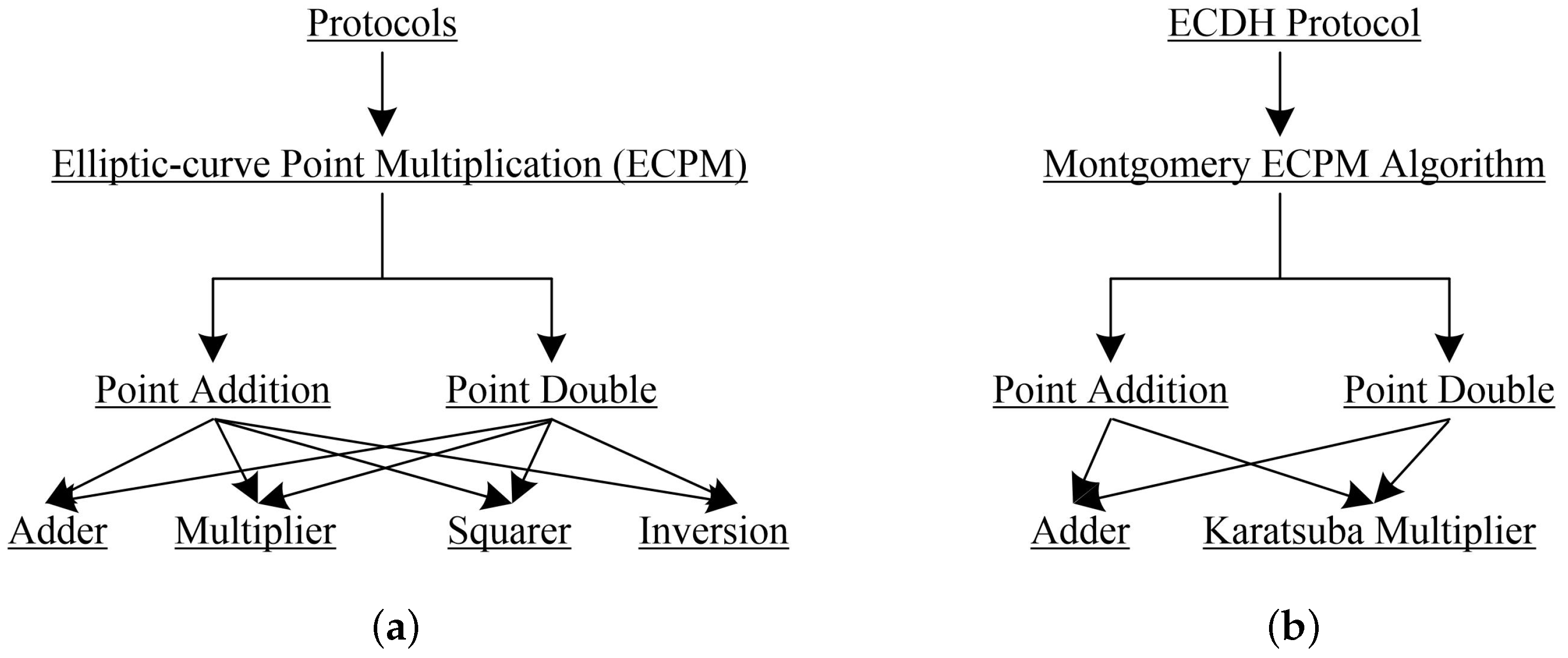
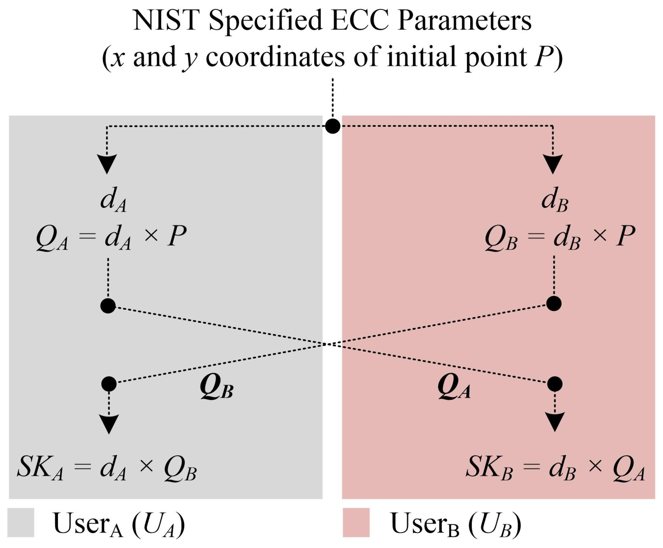
2. Related Mathematical Background

Each associated layer in Figure 1a,b requires several algorithms or protocols for cryptographic computations. Layer 1 (ECDH protocol) is responsible for a shared key generation between two different parties. As given in Figure 2, each user, i.e., U A , and U B , uses common ECC parameters to initiate the setup for a shared key generation. Moreover, each user also generates his/her public key (i.e., Q A and Q B ) by using a base-point P and his/her private key (i.e., d A and d B ). The d A and d B are m-bit random numbers (also termed as scalar multipliers and secret keys in literature). After generating the public keys, both users exchange their public keys with each other. Thereafter, the U A and U B generate their shared key using d A × Q B and d B × Q A , respectively. The A and B in the subscript of d, Q and S K (shared key) determine the execution of a corresponding operation for the respective user A and B. In Figure 2, the d × P and d × Q determine the computation of ECPM operation for U A and U B , respectively.
The computation of ECPM operation, shown in Figure 1b, is the execution of d 1 times the addition of an elliptic curve point (P) when generating the public key or (Q) when generating the shared key. To perform ECPM operations, there are several algorithms such as Double and Add, Montgomery, Lopez Dahab and many more. A comparative study over various ECPM algorithms is presented in [11]. Subsequently, the Montgomery (Algorithm 1) algorithm has been used in this work as (inherently) it provides resistance against simple power analysis (SPA) and timing attacks.
Algorithm 1: Montgomery ECPM Algorithm [12].
Applsci 12 04091 i001
Algorithm 1 contains an initial point P and a scalar multiplier d as an input. A sequence d n 1 , , d 1 , d 0 shows the bits (0 s and 1 s) of the scalar multiplier. The output of Algorithm 1 is the x and y coordinates of the generated public and shared keys. The P A d d ( ) and P D b l ( ) functions in Algorithm 1 show the instructions for point addition and double computations respectively. For i f and e l s e statements of Algorithm 1, the corresponding sequence of instructions for P A d d ( ) and P D b l ( ) functions are given below.
P A d d ( X 1 , Z 1 ) = I n s t 1 Z 1 = X 2 × Z 1 I n s t 2 X 1 = X 1 × Z 2 I n s t 3 T 1 = X 1 + Z 1 I n s t 4 X 1 = X 1 × Z 1 I n s t 5 Z 1 = T 1 2 I n s t 6 T 1 = x p × Z 1 I n s t 7 X 1 = X 1 + T 1 P D b l ( X 2 , Z 2 ) = I n s t 1 Z 2 = Z 2 2 I n s t 2 T 1 = Z 2 2 I n s t 3 T 1 = b × T 1 I n s t 4 X 2 = X 2 2 I n s t 5 Z 2 = X 2 × Z 2 I n s t 6 X 2 = X 2 2 I n s t 7 X 2 = X 2 + T 1

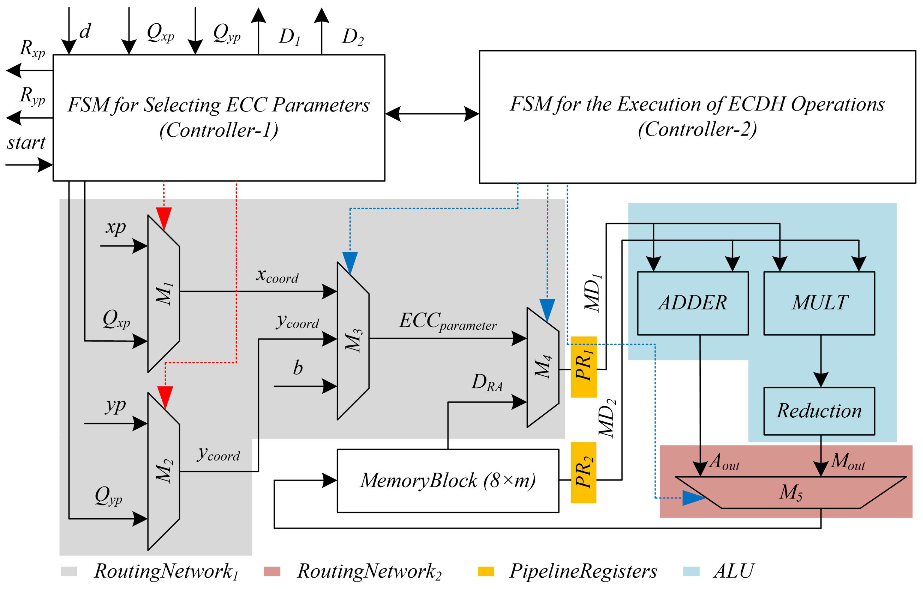
3. Proposed ECDH Architecture

The proposed ECDH architecture is shown in Figure 3. It consists of two routing networks ( R o u t i n g N e t w o r k 1 and R o u t i n g N e t w o r k 2 ), an arithmetic and logic unit (ALU), a memory unit, two pipeline registers ( P R 1 and P R 2 ) and two finite state machine based controllers (Controller-1 and Controller-2). The details of these units are given as:

3.1. Routing Networks (RoutingNetwork1 and RoutingNetwork2)

The R o u t i n g N e t w o r k 1 consists of four multiplexers, i.e., M 1 , M 2 , M 3 and M 4 . The length of M 1 , M 2 and M 4 are 2 × 1 while the length of M 3 multiplexer is 3 × 1 . The objective of M 1 and M 2 is to select coordinates of either the initial point on ECC ( x p and y p ) or coordinates of the public key ( Q x p and Q y p ) for the generation of a shared key. The multiplexer M 3 drives the output of M 1 and M 2 along with the curve constant parameter b. It is important to note that this work has utilized NIST-standardized ECC parameters ( x p , y p and b) [39]. The M 4 multiplexer is responsible to select an operand either from multiplexers M 1 , M 2 and M 3 or from an operand from the memory block. The output of M 4 goes to ALU as an input for further computations. In Figure 3, the multiplexer M 5 determines the R o u t i n g N e t w o r k 2 . The purpose of M 5 is to select an appropriate output, either after the ADDER or MULT unit, for writing back in a memory block.

3.2. Memory Block

The memory block in the proposed ECDH accelerator architecture is an 8 × m size register file. Here, the numerical value 8 denotes the total registers while the value for m determines the size of each register. The memory block is responsible for preserving the intermediate and the final results during and after the execution of Algorithm 1 and Figure 2. The internal architecture of a memory block, as shown in Figure 3, consists of two 8 × 1 multiplexers that are responsible for reading the data. Moreover, it contains one 1 × 8 demultiplexer to modify the contents of each particular register address. The Controller-2 is responsible for generating control signals to perform read and write operations.

3.3. Arithmetic and Logic Unit (ALU)

It consists of an A D D E R , M U L T and a reduction unit. The polynomial addition in G F ( 2 m ) is less complex as compared to the prime field. The implementation of an A D D E R includes an array of bitwise Exclusive (OR) gates. It bears two polynomials, i.e., M D 1 and M D 2 , as input and results an m-bit polynomial ( A o u t ) as output.
The performance of the entire crypto accelerator architecture depends on the performance of the used multiplier. Based on several polynomial multiplication techniques, described in [25], there are four possibilities to implement a multiplier circuit. These possibilities are (i) bit-serial, (ii) digit-serial, (iii) bit-parallel and (iv) digit-parallel. For two m bit input operands, the bit-serial multipliers require m clock cycles for computation. A schoolbook multiplication method is a typical example of bit-serial multiplication. In digit-serial multipliers, p q clock cycles are required for one polynomial multiplication, where p determines the operand length and q is the digit size. Moreover, the computational cost in bit/digit parallel multipliers is one clock cycle. Based on the clock cycles requirement of several multiplication approaches, as discussed in [25], the bit-serial multipliers are suitable for area-constrained applications. Similarly, the bit/digit parallel multipliers are useful for high-speed cryptographic applications. Finally, the digit-serial multiplication approaches are more convenient where the speed and hardware resources are simultaneously important.
Based on the aforementioned discussion, we have implemented a bit-parallel Karatsuba multiplier over G F ( 2 233 ) . The mathematical structure (in the simplest way) to perform Karatsuba multiplication is explained in [22]. It uses the splitting of m bit input polynomials into two m / 2 bit polynomials. Each m / 2 bit polynomial is further divided into two smaller polynomials ( m / 4 bit). This division is duplicated until the smaller polynomials for multiplication are acquired. After dividing polynomials, the resultant polynomial is generated by performing multiplication in chronological order. For further descriptions, we refer interested readers to [22]. In short, the Karatsuba multiplier in M U L T unit takes two polynomials ( M D 1 and M D 2 ) as input and results in 2 × m 1 bit polynomial ( M o u t ) as output. It is important to note that the size of the resultant polynomial generated after the M U L T unit is 2 × m 1 bit (not shown in Figure 3). Therefore, in this work, the reduction from 2 × m 1 bit to m bit is performed using a NIST-recommended polynomial reduction algorithm (see Algorithm 2.41 of [14]).
The P A d d and P D b l functions in Algorithm 1 requires some squaring instructions (e.g., I n s t 5 in P A d d while I n s t 1 , I n s t 2 , I n s t 4 and I n s t 6 in P D b l ). In our work, these squaring instructions are computed by providing similar inputs to the Karatsuba multiplier as performed in [12]. Subsequently, this shows a decrease in hardware resources without affecting the clock cycles. As shown in Algorithm 1, the reconversion from projective to affine needs two polynomial inversion computations. There are several inversion methods in the literature to perform the multiplicative inverse of the polynomials. However, the Itoh–Tsujii inversion algorithm is more frequently utilized in state-of-the-art approaches as it requires only the multiplications and square operations for the computation [12,18,19]. Therefore, in our implementation, we have utilized the hardware resources of our M U L T unit to perform the polynomial inversion using the square Itoh–Tsujii algorithm.
The Itoh–Tsujii inversion algorithm over G F ( 2 233 ) requires ten polynomial multiplications followed by m 1 squares [40]. Each multiplication over G F ( 2 233 ) using the Karatsuba multiplier is accomplished in one clock cycle. Therefore, ten multiplications require ten clock cycles. The m 1 clock cycles are required for the squaring as one square takes only the one clock cycle. The total clock cycles to perform one inversion are ( 10 + m 1 ) . Using our ECDH architecture (given in Figure 3), 2 × ( 10 + m 1 ) clock cycles are needed to perform one polynomial inversion over G F ( 2 233 ) because we used only the one M U L T unit for both multiplication and squaring computations. On the other hand, the Itoh–Tsujii requires repeated squaring computations. Apart from one M U L T unit, we have employed the pipeline registers in the proposed ECDH design. These two factors (use of one M U L T and pipelining) determine the limitation of our architecture for the inversion computation.

3.4. Pipeline Registers and Scheduling

The inclusion of pipeline registers increases clock frequency and reduces the critical path of the proposed ECDH architecture. There are several choices for the inclusion of pipeline registers in the proposed ECDH architecture (given in Figure 3). For example, one pipeline register after M 1 , M 2 , M 3 , D R A , M 4 , M e m o r y B l o c k and M 5 resulting a five-stage pipeline architecture. With this register placement, instruction read is performed in three clock cycles. Two cycles are needed to perform instruction execution and write back operations. As one can see, the instruction read takes three clock cycles which is not an optimal choice. With this observation, we decrease the number of pipeline stages from five to four. The synthesis results show a similar clock frequency as compared to five-stage pipelining. We repeated this process until a two-stage pipelining is reached (It is important to note that the inclusion of more pipeline registers (i.e., from two-stage to three-stage and so on) is no longer beneficial in our architecture. More than two-stage pipelining results in a significant increase in the hardware resources but with a minor increase in the clock frequency). Therefore, in our proposed ECDH architecture (shown in Figure 3), we have included two pipeline registers (only) on the inputs of the ALU (one after M 4 and another after M e m o r y B l o c k ). It requires reading ([R]) in one clock cycle and both executing and writing back ([EWB]) in another cycle.
The instructions for P A d d and P D b l functions of Algorithm 1 in a two-stage pipelining are shown in Table 1. Column one provides the clock cycles (CCs). The original instructions for P A d d and P D b l functions of Algorithm 1 are shown in column two. Columns three to five provide the status of instructions for P A d d and P D b l functions in a two-stage pipelining without the proposed scheduling. Finally, the last three columns (six to eight) provide the proposed scheduling for the instructions of P A d d and P D b l functions in a two-stage pipelining.
Table 1 shows that the instructions of P A d d and P D b l functions of Algorithm 1 requires 22 CCs. Moreover, in two-stage pipelining, there are read-after-write (RAW) hazards when executing these instructions. It implies that the execution of the current instruction is stopped until the write-back of the previous instruction is finished. For example, in the first clock cycle, operands of P A d d I n s t 1 are fetched from the memory unit. In the next cycle, operands for P A d d I n s t 2 are fetched while the execution and write-back of P A d d I n s t 1 are completed. In clock cycle three, P A d d I n s t 3 can not be fetched because it depends on the result of previous instruction ( P A d d I n s t 2 ). This is termed the RAW hazard. In total, seven RAW hazards (shown in column five of Table 1) are occurred when the instructions of P A d d and P D b l functions are executed sequentially.
To reduce the RAW hazards or to reduce the total number of clock cycles, an efficient scheduling technique is presented for the instructions of P A d d and P D b l functions. The proposed scheduling is shown in the last three columns of Table 1. We can observe in column six that the operands for P D b l I n s t 1 are fetched from the memory unit in clock cycle three. It allows reducing the clock cycles (total 17) for the execution of one P A d d and P D b l operation. To summarize, the instructions for P A d d and P D b l functions of Algorithm 1 require 22 × m clock cycles in a two-stage pipelining when no scheduling is considered for executions. Here, m is the key length (233 in this work). However, with the proposed scheduling, the required number of clock cycles for the execution of one P A d d and P D b l functions are 17 × m . Therefore, the proposed scheduling scheme reduces 5 × m clock cycles.

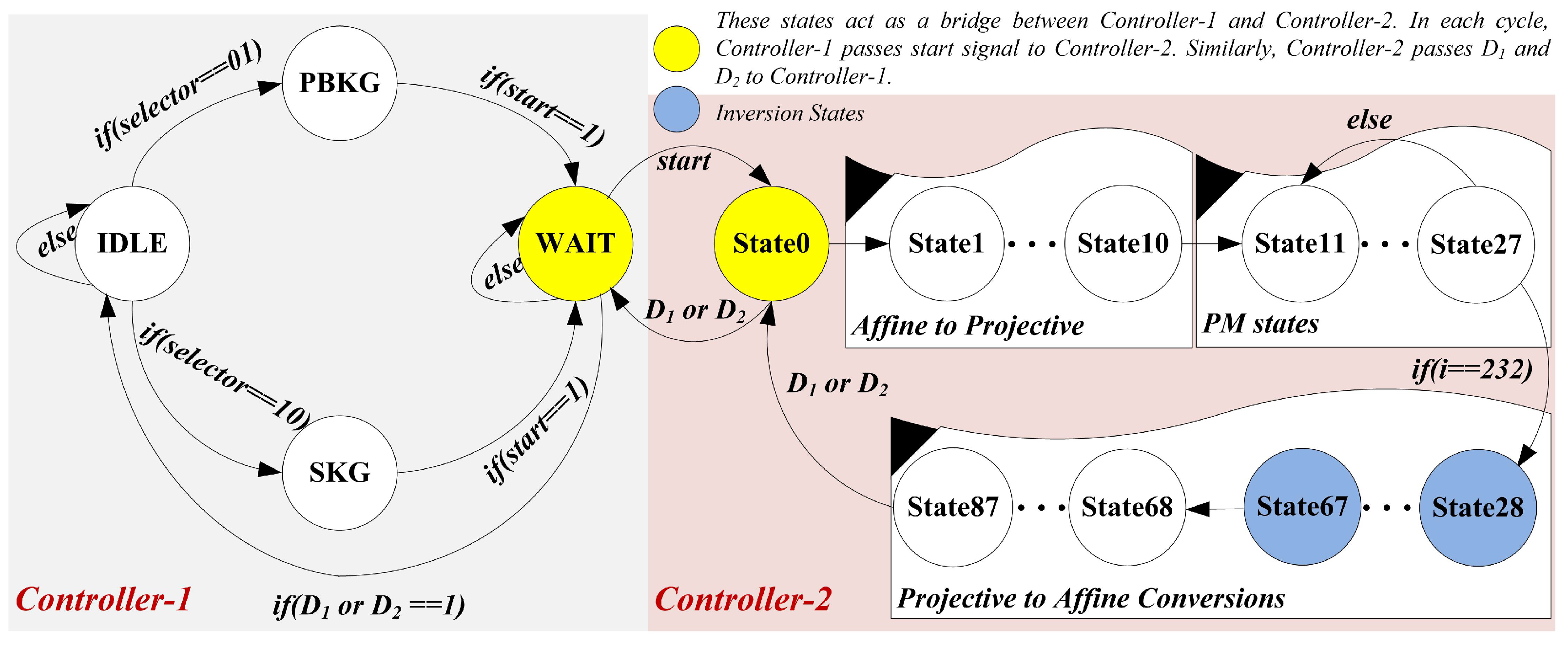
3.5. Dedicated FSM Controllers

As shown in Figure 3, two FSM controllers (Controller-1 and Controller-2) are used. The intent to use two controllers is to attain the minimum routing delays. In other words, a single FSM having a larger number of states results in longer routing delays [41]. Therefore, the Controller-1 operates like a wrapper for Controller-2. More precisely, Controller-1 provides the ECC parameters in terms of coordinates of either initial point P or public key Q as an input to Controller-2. After providing the input parameters, the Controller-1 stays in a WAIT state until the Controller-2 responds. More insightful details of these controllers are given as:

3.5.1. Controller-1

It is responsible for generating control signals for M 1 and M 2 routing multiplexers. The generated control signals are shown with the red color dotted lines in Figure 3. The inputs/outputs to/from Controller-1 are also shown in Figure 3. One of the input to Controller-1 is d which is an m-bit secret key or a scalar multiplier, given in Algorithm 1. Similarly, two other inputs, i.e., Q x p , and Q y p , hold the x and y coordinates for a public key of another party during the shared key generation. An s t a r t signal triggers the processor to initiate the computation process. The R x p and R y p provide x and y coordinates respectively. In addition to it, the D 1 and D 2 are one-bit done signals. The D 1 reveals that the public key is generated while the D 2 shows that the shared key is generated. The corresponding D 1 and D 2 signals are generated after the required computation by Controller-2. As shown in Figure 4, Controller-1 incorporates a total of four states, i.e., I D L E , P B K G , S K G and W A I T . As the name implies, P B K G determines the public key generation while S K G means the shared key generation. Consequently, descriptions of these states are as follows:
(i)
State one is an I D L E state. Based on the s e l e c t o r signal (not shown in Figure 3), the processor shifts from I D L E state to either in P B K G or S K G . Otherwise, the processor remains in the I D L E state.
(ii)
In the P B K G state, the processor checks the s t a r t signal. Once it becomes true, the Controller-1 generates the control signals to select x p and y p coordinates of initial point P.
(iii)
Similarly, the processor checks the s t a r t signal in state three ( S K G ). Once it becomes true, it generates the control signals to choose x p and y p coordinates of a public key Q.
(iv)
After generating control signals either in-state P B K G or S K G , the next state becomes state four ( W A I T ). The W A I T state determines that the processor is now waiting for the done signals (either for D 1 or D 2 ) from Controller-2. Whenever the processor switches its state from P B K G to W A I T , it implies that the processor is generating coordinates for a public key. Whenever the processor changes its state from S K G to W A I T , it denotes that the processor is computing coordinates for a shared key. It is important to note that the transformation, either from P B K G to W A I T or from S K G to W A I T , the proposed architecture consumes one clock cycle. The clock cycles for the W A I T state depends on the required cycles for Controller-2 to set the D 1 or D 2 signals. Therefore, Equation (1) provides the total number of clock cycles for our ECDH architecture.
ECDH cycles = 2 + 2 ( PM cycles )
In Equation (1), one clock cycle is required for transformation from I D L E state to either in P B K G or S K G . Another clock cycle is needed for shifting either from P B K G or S K G to the W A I T state. The clock cycles calculation for PMcycles will be discussed briefly in the next section.

3.5.2. Controller-2

It is responsible for generating control signals for the computation of Q = d × P and S K = d × Q using Algorithm 1. The mathematical formulations are shown earlier in Figure 2. As presented in Figure 4, the three steps ((i) affine to projective conversions, (ii) PM in projective coordinates and (iii) reconversions from projective to affine) of Algorithm 1 constitute a total of 88 states (states 0 to 87). The details for the corresponding states are as follows:
(i)
The initial state (state 0) is idle. When Controller-2 receives the s t a r t signal (as 1) from Controller-1, it starts generating the control signals for projective to affine conversions. It requires 10 states from state 1 to 10 such that each state takes one clock cycle for computation. In other words, the proposed ECDH architecture takes 10 clock cycles for affine to projective conversions.
(ii)
Fourteen instructions of P A d d (seven) and P D b l (seven) functions of Algorithm 1 are operated in seventeen states (state 11 to 27). The reason for more states is the two-stage pipelining. The details of pipelining are given in Table 1 of Section 3.4). During each state, the value for an inspected key bit, i.e., d i , is checked. When the inspected value for d i becomes 1, the i f part from Algorithm 1 is implemented. Otherwise, the e l s e part is operated. These 17 states are operated in 17 clock cycles and are repeated until the condition for the l o o p statement of Algorithm 1 becomes true. When it becomes true, the processor switches control from PM to the reconversions step.
(iii)
The states from 28 to 87 are responsible for projective to affine conversions. In states 28 to 67, a polynomial inversion is computed. For one inversion computation, our ECDH design takes 2 ( 10 + m 1 ) clock cycles. As shown in Algorithm 1, the projective to affine conversions require two inversion computations. Therefore, the cost for two inversion operations is 4 ( 10 + m 1 ) . Moreover, some additional states are needed (from 68 to 87) to accomplish the remaining operations of projective to affine conversions.
To summarize, the total number of clock cycles for the computation of Q = d × P and S K = d × Q are calculated using Equation (2). It reveals that the affine to projective conversion requires 10 clock cycles. The PM computation in projective coordinates requires 17 ( m 1 ) clock cycles. The projective to affine conversion process requires 4 ( 10 + m 1 ) cycles for two inversion computations and additional 20 cycles for the completion of the remaining operations in the process. Consequently, the proposed ECDH architecture over G F ( 2 m ) with m = 233 requires 4942 clock cycles for one PM computation (i.e., Q = d × P , and S K = d × Q ).
PM cycles = 10 + 17 ( m 1 ) + 4 ( 10 + m 1 ) + 20

4. Results and Comparisons

4.1. Results

The proposed ECDH architecture is implemented in Verilog language using the Vivado IDE (Integrated Design Environment) tool. For performance evaluations, the implementation results are presented on different FPGA devices, i.e., Virtex-7 (xc7vx690tffg1930-2), Spartan-7 (xc7s100fgga676-2), Artix-7 (xc7a200tsbv484-2) and Kintex-7 (xc7k480tffv1156-2). The respective details for the targeted FPGA devices are given in [42]. The achieved results are given in Table 2.
Column one of Table 2 provides the targeted device. The utilized area (in terms of slices, look-up tables (LUTs) and flip-flops (FFs)) is shown in columns two, three and four respectively. The area information is obtained directly from the Vivado tool. Similar to the reported area values, the operational frequency (Freq in MHz) is also acquired from the tool and is presented in column five of Table 2. Columns six and seven show the CCs and latency (in μs) information for one PM computation. Similarly, columns eight and nine present the clock cycles and latency (in μs) information for one shared key generation. The clock cycles for one shared key generation are calculated from Equation (1). Likewise, the clock cycles for one PM computation are calculated from Equation (2).
The latency is the time required to execute one crypto operation (either public or shared key generation in this work). The latency values are calculated using Equation (3). To provide a realistic tradeoff over different FPGA devices, we have defined a figure-of-merit (FoM) in terms of the ratio of throughput over FPGA slices. The FoM values are reported for the shared key generation, as shown in the last column of Table 2. The throughput is the ratio of one over latency and is calculated using Equation (4). Finally, the FoM values are calculated using Equation (5).
Latency ( in μ s ) = Clock Cycles Frequency ( in MHz )
Throughput = 1 Latency ( in μ s ) = 10 6 Latency ( in s )
FoM = Throughput FPGA slices
Table 2 shows the trend for hardware resource utilization on various 28 nm implementation technologies. Therefore, the minimum hardware resources (5102 slices, 12,339 LUTs and 2459 FFs) are obtained for the Virtex-7 device when compared to Spartan-7, Artix-7 and Kintex-7 devices. The utilized FPGA slices for Spartan-7, Artix-7 and Kintex-7 devices are 5634, 5957 and 6102. Similar to hardware resource utilization, the highest clock frequency of 318 MHz is achieved on Virtex-7 FPGA. On Spartan-7 (312 MHz), Artix-7(316 MHz) and Kintex-7(304 MHz) devices, we also acquired the closest clock frequency to our Virtex-7 implementations. When trading from Virtex-7 to Kintex-7 implementations, the minor increase in the FPGA slices and clock frequency indicates the efficiency of our architecture. The times to generate one public key on Virtex-7, Spartan-7, Artix-7 and Kintex-7 are 15.54 μs, 15.83 μs, 15.63 μs and 16.25 μs. On similar FPGA devices, the times to generate one shared key are 31.08 μs, 31.68 μs, 31.28 μs and 32.51 μs.
The defined FoM determines the performance of our crypto architecture on different 28 nm implementation technologies. The higher the FoM value, the higher will be the performance of the crypto architecture. Consequently, the highest 6.30 FoM value is calculated for Virtex-7 FPGA. For Spartan-7, Artix-7 and Kintex-7 devices, the calculated values for FoM are 5.60, 5.36 and 5.04.

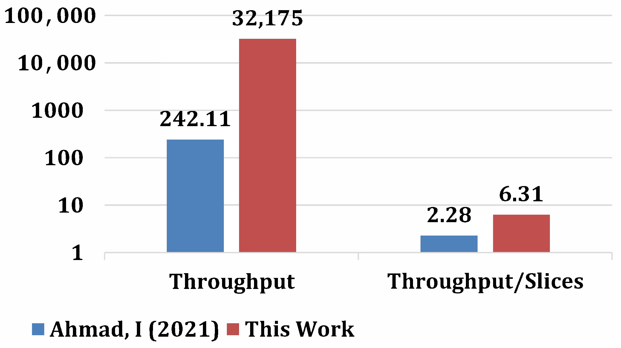
4.2. Comparisons with State-of-the-Art

The ECPM designs of [12,17,19] support only the PM operation, without the consideration of the topmost layer of ECC (protocol layer). In other words, there are very few hardware designs that enfold the implementation of ECDH protocol on a reconfigurable FPGA. The comparison to state-of-the-art architectures is shown in Table 3. Column one indicates the reference to existing hardware implementations of the ECDH protocol. Column two offers the implemented ECC model in addition to the used algorithms for the execution of either public or shared key generation. The targeted FPGA device used for the implementation is shown in column three. We have evaluated the FPGA slices for hardware resource comparisons. The corresponding hardware resources are presented in column four. The timing details (in terms of clock frequency (MHz) and latency (μs)) for generating a single shared key are presented in the last two columns (five and six) respectively.
Comparison with [17,19,31] over G F ( 2 163 ) on Virtex-7 and Kintex-7 FPGA. On Virtex-7 FPGA, our ECDH architecture takes 2.28 (ratio of 11,657 over 5102) times lower FPGA slices as compared to the low-latency ECPM design of [17]. Moreover, our design with a 233-bit key length achieves a 2 (ratio of 318 over 159) times higher clock frequency. When comparing the latency, the architecture of [17] is 5.49 (ratio of 15.54 over 2.83) times more efficient as compared to our work. The reason for this efficiency is the different supported key lengths (233 in our work while a 163 in [17]—see column two in Table 3). Another ECPM architecture on Virtex-7 is reported in [19]. Due to distinct key lengths, their design consumes lower FPGA slices (3657) when compared to our 233-bit design (5102). On the contrary, our ECDH architecture achieves 2.35 (ratio of 318 over 135) times higher clock frequency. Additionally, the ECPM design of [19] requires 2 (ratio of 25.3 over 15.54) times higher computational time (latency) as compared to our ECDH design.
On Kintex-7 FPGA, the architecture of [31] utilizes 2.70 (ratio of 6102 over 2253) times lower FPGA slices as compared to our Kintex-7 implementation. The cause for the use of lower slices in [31] is the use of lower key-length (i.e., 163). An additional reason is the use of a simple Double and Add PM algorithm which is vulnerable to simple power analysis attacks (a type of side-channel attack) for the general Weierstrass form of elliptic curves. On the other hand, we employed a Montgomery PM algorithm which is inherently subjected to simple power analysis attacks even if the Weierstrass form of elliptic curves is used. Although we utilize a higher key length (i.e., 233), our design achieves a comparable clock frequency of 304 MHz while 306 MHz is obtained in [31] over a 163-bit key length. Moreover, our proposed PM architecture requires lower computational time because we used projective coordinates for the execution of PM operation whereas a simple affine coordinate system is used in [31].
Comparison with [12] over G F ( 2 233 ) on Virtex-7 FPGA. On Virtex-7 FPGA, a two-stage pipeline design of [12] utilizes 1.09 (ratio of 5120 over 5102) times higher slices as compared to our two-stage pipelined architecture. Similar to hardware resources, the architecture of [12] requires higher computational time as compared to this work (given in the last column of Table 3). On the other hand, the ECPM architecture of [12] is 1.12 (ratio of 357 over 318) times faster in terms of clock frequency as compared to our design. The reason is the support for all the ECC layers in our design while the protocol layer is not considered for implementation in [12].
Comparison with ECDH design of [35] over G F ( 2 233 ) on Virtex-7 FPGA. Although, our design utilizes 2.82 (ratio of 4763 over 1809) times higher slices on Virtex-7 FPGA when compared to the most recent ECDH architecture of [35], however, it is 5.08 (ratio of 318 over 62.5) times faster in terms of clock frequency. The latency requirement of the presented architecture is 132.88 (ratio of 4130 over 31.08) times lower as compared to the most recent design. Moreover, we have compared our FoM results with only the design of [35] as this architecture is specifically described for the ECDH implementation. Therefore, the calculated FoM values are illustrated in Figure 5. It shows that the proposed ECDH accelerator architecture results in higher throughput. Moreover, the proposed dedicated crypto processor architecture is 2.76 (ratio of 6.31 over 2.28) times faster in the context of t h r o u g h p u t a r e a .
Comparison with architecture of [33] over ECDH + SIKEX434 algorithms on Artix-7 FPGA. Our ECDH architecture utilizes 3.58 (ratio of 5957 over 1663) times lower FPGA slices. The reasons for the use of higher hardware resources in our work are (i) pipelining and (ii) a bit-parallel Karatsuba multiplier for multiplying polynomial coefficients. On the other hand, our ECDH design achieves 1.62 (ratio of 316 over 195) times higher clock frequency as we employed two-stage pipelining to reduce the critical path of the proposed architecture. Moreover, our design is 396.6 (ratio of 6200 over 15.63) times faster in terms of computational time (i.e., latency). There is always a tradeoff between hardware area and performance (in terms of clock frequency or latency).
Comparison with design of [32] over Ed25519 + X25519 curves on Artix-7 FPGA. The proposed ECDH design is 1.85 (ratio of 5957 over 3204) times more area efficient in terms of FPGA slices. Moreover, due to 2-stage pipelining, our ECDH architecture is 3.85 (ratio of 316 over 82) times faster in terms of operational frequency. The comparison to latency is not possible to provide as the relevant information is not described in [32].

4.3. Significance of This Work

The implementation results reported for our proposed t h r o u g h p u t a r e a architecture on different 7-series FPGA devices reveal the suitability of this work in applications that demand key authentication before starting communications. The typical examples include the IoTs, health-related applications, smart cards, automotive mobile/vehicles, etc. More precisely, the IoT nodes require key authentication prior to starting communications [7,8,10]. Moreover, in modern health care systems [1], authentication is needed to retrieve data securely on an unsecured cloud. The V2X needs authentication to start secure communication over the network/cloud [2]. Authentication is needed to make online payments in the case of smart cards. The identification of a human using his/her smart ID card is another application where authentication is essential. Based on [43,44], the aforementioned applications require low-power for data transmission and authentication purposes. We believe the reported values for high throughput and low area, in this work, result in low power. Therefore, our proposed design could be beneficial for secure communication in IoT-related applications, where both throughput and area parameters are desired for cryptographic computations.

5. Conclusions

This paper has presented a shared key generation architecture using the ECDH protocol of ECC over G F ( 2 233 ) with the consideration of high-speed and low-area at the same time. A 2-stage pipelining and a Karatsuba multiplier are incorporated to achieve high speed. The employed pipelining has reduced the critical path and improved clock frequency. Similarly, the utilization of the Karatsuba multiplier has decreased clock cycles. Towards the low-area goal, singular adder and multiplier units are included for arithmetic operations. These operations are addition, multiplication, squaring (providing similar inputs to the multiplier) and inversion (using the Itoh–Tsujii algorithm). This strategy has ultimately helped us to reduce the hardware resources. Two FSM-based dedicated controllers are employed for efficient control functionalities. The implementation results after place-and-route are provided on Virtex-7, Spartan-7, Artix-7 and Kintex-7 FPGA devices. Over G F ( 2 233 ) , the utilized FPGA slices are 5102 (Virtex-7), 5634 (Spartan-7), 5957 (Artix-7) and 6102 (Kintex-7). The computational time for one shared key generation is 31.08 (Virtex-7), 31.68 (Spartan-7), 31.28 (Artix-7) and 32.51 (Kintex-7). The proposed ECDH architecture outperforms others on Virtex-7 FPGA in terms of t h r o u g h p u t a r e a ( F P G A s l i c e s ) (the achieved value is 6.30). Moreover, it has been shown that the proposed architecture is 302.7 and 132.88 times faster in terms of latency as compared to state-of-the-art ECDH designs of [35,38], respectively. The achieved results and performance comparison statistics reveal the suitability of the proposed architecture in high-speed with low-area key agreement applications.

Author Contributions

Conceptualization, M.R. and A.A.; data extraction, S.Z.K. and Z.M.; results compilation, M.R. and S.Z.K.; validation, M.R. and Z.M.; writing—original draft preparation, S.Z.K. and H.K.; critical review, M.R. and I.B.; draft optimization, S.Z.K. and H.K.; supervision, M.R.; funding acquisition, A.A. All authors have read and agreed to the published version of the manuscript.

Funding

We are thankful for the support of the Deanship of Scientific Research at King Khalid University, Abha, Saudi Arabia for funding this work under grant number R.G.P.2/132/42.

Institutional Review Board Statement

Not applicable.

Informed Consent Statement

Not applicable.

Conflicts of Interest

The authors declare no conflict of interest.

References

  1. Ding, D.; Conti, M.; Solanas, A. A smart health application and its related privacy issues. In Proceedings of the 2016 Smart City Security and Privacy Workshop (SCSP-W), Vienna, Austria, 11 April 2016; pp. 1–5. [Google Scholar] [CrossRef]
  2. Kornaros, G.; Tomoutzoglou, O.; Mbakoyiannis, D.; Karadimitriou, N.; Coppola, M.; Montanari, E.; Deligiannis, I.; Gherardi, G. Towards holistic secure networking in connected vehicles through securing CAN-bus communication and firmware-over-the-air updating. J. Syst. Archit. 2020, 109, 101761. [Google Scholar] [CrossRef]
  3. Mun, H.; Han, K.; Lee, D.H. Ensuring Safety and Security in CAN-Based Automotive Embedded Systems: A Combination of Design Optimization and Secure Communication. IEEE Trans. Veh. Technol. 2020, 69, 7078–7091. [Google Scholar] [CrossRef]
  4. Xie, G.; Li, R.; Hu, S. Security-Aware Obfuscated Priority Assignment for CAN FD Messages in Real-Time Parallel Automotive Applications. IEEE Trans. Comput.-Aided Des. Integr. Circuits Syst. 2020, 39, 4413–4425. [Google Scholar] [CrossRef]
  5. Chandramouli, R.; Lee, P. Infrastructure Standards for Smart ID Card Deployment. IEEE Secur. Priv. 2007, 5, 92–96. [Google Scholar] [CrossRef]
  6. Premila Bai, T.D.; Raj, K.M.; Rabara, S.A. Elliptic Curve Cryptography Based Security Framework for Internet of Things (IoT) Enabled Smart Card. In Proceedings of the 2017 World Congress on Computing and Communication Technologies (WCCCT), Tiruchirappalli, India, 2–4 February 2017; pp. 43–46. [Google Scholar] [CrossRef]
  7. Vinoth, R.; Deborah, L.J.; Vijayakumar, P.; Kumar, N. Secure Multifactor Authenticated Key Agreement Scheme for Industrial IoT. IEEE Internet Things J. 2021, 8, 3801–3811. [Google Scholar] [CrossRef]
  8. Srinivas, J.; Das, A.K.; Wazid, M.; Kumar, N. Anonymous Lightweight Chaotic Map-Based Authenticated Key Agreement Protocol for Industrial Internet of Things. IEEE Trans. Dependable Secur. Comput. 2020, 17, 1133–1146. [Google Scholar] [CrossRef]
  9. Sahu, A.K.; Sharma, S.; Puthal, D. Lightweight Multi-Party Authentication and Key Agreement Protocol in IoT-Based E-Healthcare Service. ACM Trans. Multimedia Comput. Commun. Appl. 2021, 17, 64. [Google Scholar] [CrossRef]
  10. Rahman, M.S.; Hossam-E-Haider, M. Quantum IoT: A Quantum Approach in IoT Security Maintenance. In Proceedings of the 2019 International Conference on Robotics, Electrical and Signal Processing Techniques (ICREST), Dhaka, Bangladesh, 10–12 January 2019; pp. 269–272. [Google Scholar] [CrossRef]
  11. Rashid, M.; Imran, M.; Jafri, A.R.; Al-Somani, T.F. Flexible Architectures for Cryptographic Algorithms—A Systematic Literature Review. J. Circuits Syst. Comput. 2019, 28, 1930003. [Google Scholar] [CrossRef]
  12. Imran, M.; Rashid, M.; Jafri, A.R.; Kashif, M. Throughput/area optimised pipelined architecture for elliptic curve crypto processor. IET Comput. Digit. Tech. 2019, 13, 361–368. [Google Scholar] [CrossRef] [Green Version]
  13. Bansal, M.; Gupta, S.; Mathur, S. Comparison of ECC and RSA Algorithm with DNA Encoding for IoT Security. In Proceedings of the 2021 6th International Conference on Inventive Computation Technologies (ICICT), Coimbatore, India, 20–22 January 2021; pp. 1340–1343. [Google Scholar] [CrossRef]
  14. Hankerson, D.; Menezes, A.J.; Vanstone, S. Guide to Elliptic Curve Cryptography; Springer: New York, NY, USA, 2004; pp. 1–311. Available online: https://0-link-springer-com.brum.beds.ac.uk/book/10.1007/b97644 (accessed on 13 August 2021).
  15. Liusvaara, I. CFRG Elliptic Curve Diffie-Hellman (ECDH) and Signatures in JSON Object Signing and Encryption (JOSE). RFC 8037. 2017. Available online: https://www.rfc-editor.org/info/rfc8037 (accessed on 7 January 2022).
  16. Rashidi, B. Low-Cost and Fast Hardware Implementations of Point Multiplication on Binary Edwards Curves. In Proceedings of the Iranian Conference on Electrical Engineering (ICEE), Mashhad, Iran, 8–10 May 2018; pp. 17–22. [Google Scholar] [CrossRef]
  17. Khan, Z.U.A.; Benaissa, M. High-Speed and Low-Latency ECC Processor Implementation Over GF(2m) on FPGA. IEEE Trans. Very Large Scale Integr. (VLSI) Syst. 2017, 25, 165–176. [Google Scholar] [CrossRef] [Green Version]
  18. Khan, Z.U.A.; Benaissa, M. Low area ECC implementation on FPGA. In Proceedings of the 2013 IEEE 20th International Conference on Electronics, Circuits, and Systems (ICECS), Abu Dhabi, United Arab Emirates, 8–11 December 2013; pp. 581–584. [Google Scholar] [CrossRef]
  19. Imran, M.; Rashid, M.; Shafi, I. Lopez Dahab based elliptic crypto processor (ECP) over GF(2163) for low-area applications on FPGA. In Proceedings of the 2018 International Conference on Engineering and Emerging Technologies (ICEET), Lahore, Pakistan, 22–23 February 2018; pp. 1–6. [Google Scholar] [CrossRef]
  20. Batina, L.; Mentens, N.; Ors, S.; Preneel, B. Serial multiplier architectures over GF(2/sup n/) for elliptic curve cryptosystems. In Proceedings of the 12th IEEE Mediterranean Electrotechnical Conference (IEEE Cat. No.04CH37521), Dubrovnik, Croatia, 12–15 May 2004; Volume 2, pp. 779–782. [Google Scholar] [CrossRef]
  21. Kodali, R.K.; Gomatam, P.; Boppana, L. FPGA implementation of multipliers for ECC. In Proceedings of the 2014 2nd International Conference on Emerging Technology Trends in Electronics, Communication and Networking, Surat, India, 26–27 December 2014; pp. 1–5. [Google Scholar] [CrossRef]
  22. Imran, M.; Abideen, Z.U.; Pagliarini, S. An Open-source Library of Large Integer Polynomial Multipliers. In Proceedings of the 2021 24th International Symposium on Design and Diagnostics of Electronic Circuits Systems (DDECS), Vienna, Austria, 7–9 April 2021; pp. 145–150. [Google Scholar] [CrossRef]
  23. Heidarpur, M.; Mirhassani, M. An Efficient and High-Speed Overlap-Free Karatsuba-Based Finite-Field Multiplier for FGPA Implementation. IEEE Trans. Very Large Scale Integr. (VLSI) Syst. 2021, 29, 667–676. [Google Scholar] [CrossRef]
  24. Lee, C.Y.; Zeghid, M.; Sghaier, A.; Ahmed, H.Y.; Xie, J. Efficient Hardware Implementation of Large Field-Size Elliptic Curve Cryptographic Processor. IEEE Access 2022, 10, 7926–7936. [Google Scholar] [CrossRef]
  25. Imran, M.; Rashid, M. Architectural review of polynomial bases finite field multipliers over GF(2m). In Proceedings of the 2017 International Conference on Communication, Computing and Digital Systems (C-CODE), Islamabad, Pakistan, 8–9 March 2017; pp. 331–336. [Google Scholar] [CrossRef]
  26. Gaudry, P. Index Calculus for Abelian Varieties and the Elliptic Curve Discrete Logarithm Problem. Cryptology ePrint Archive, Report 2004/073. 2004. Available online: https://ia.cr/2004/073 (accessed on 4 January 2022).
  27. Petit, C.; Quisquater, J.J. On Polynomial Systems Arising from a Weil Descent. Cryptology ePrint Archive, Report 2012/146. 2012. Available online: https://ia.cr/2012/146 (accessed on 19 January 2022).
  28. Chen, L.; Moody, D.; Regenscheid, A. Recommendations for Discrete Logarithm-Based Cryptography: Elliptic Curve Domain Parameters. Available online: https://nvlpubs.nist.gov/nistpubs/SpecialPublications/NIST.SP.800-186-draft.pdf (accessed on 4 April 2022).
  29. Raso, O.; Mlynek, P.; Fujdiak, R.; Pospichal, L.; Kubicek, P. Implementation of Elliptic Curve Diffie Hellman in ultra-low power microcontroller. In Proceedings of the 2015 38th International Conference on Telecommunications and Signal Processing (TSP), Prague, Czech Republic, 9–11 July 2015; pp. 662–666. [Google Scholar] [CrossRef]
  30. Fujdiak, R.; Misurec, J.; Mlynek, P.; Leonard, J. Cryptograph key distribution with elliptic curve Diffie-Hellman algorithm in low-power devices for power grids. Rev. Roum. Sci. Tech. 2016, 61, 84–88. [Google Scholar]
  31. Hossain, M.S.; Saeedi, E.; Kong, Y. High-performance FPGA Implementation of Elliptic Curve Cryptography Processor over Binary Field GF(2163). In Proceedings of the 2nd International Conference on Information Systems Security and Privacy (ICISSP 2016), Rome, Italy, 19–21 February 2016; pp. 415–422. [Google Scholar] [CrossRef] [Green Version]
  32. Turan, F.; Verbauwhede, I. Compact and Flexible FPGA Implementation of Ed25519 and X25519. ACM Trans. Embed. Comput. Syst. 2019, 18, 24. [Google Scholar] [CrossRef]
  33. Azarderakhsh, R.; Khatib, R.E.; Koziel, B.; Langenberg, B. Hardware Deployment of Hybrid PQC. Cryptology ePrint Archive, Report 2021/541. 2021. Available online: https://ia.cr/2021/541 (accessed on 24 December 2021).
  34. Ionita, D.M.; Simion, E. FPGA Offloading for Diffie-Hellman Key Exchange Using Elliptic Curves. Cryptology ePrint Archive, Report 2021/065. 2021. Available online: https://ia.cr/2021/065 (accessed on 26 December 2021).
  35. Ahmad, I.; Morales-Sandoval, M.; Flores, L.A.R.; Cumplido, R.; Garcia-Hernandez, J.J.; Feregrino, C.; Algredo, I. A Compact FPGA-Based Accelerator for Curve-Based Cryptography in Wireless Sensor Networks. J. Sens. 2021, 2021, 8860413. [Google Scholar] [CrossRef]
  36. Yang, P.; Xiong, N.; Ren, J. Data Security and Privacy Protection for Cloud Storage: A Survey. IEEE Access 2020, 8, 131723–131740. [Google Scholar] [CrossRef]
  37. Rawal, B.S.; Vivek, S.S. Secure Cloud Storage and File Sharing. In Proceedings of the 2017 IEEE International Conference on Smart Cloud (SmartCloud), New York, NY, USA, 3–5 November 2017; pp. 78–83. [Google Scholar] [CrossRef]
  38. Fournaris, A.P.; Zafeirakis, I.; Koulamas, C.; Sklavos, N.; Koufopavlou, O. Designing efficient elliptic Curve Diffie-Hellman accelerators for embedded systems. In Proceedings of the 2015 IEEE International Symposium on Circuits and Systems (ISCAS), Lisbon, Portugal, 24–27 May 2015; pp. 2025–2028. [Google Scholar] [CrossRef]
  39. NIST. Recommended Elliptic Curves for Federal Government Use. 1999. Available online: https://csrc.nist.gov/csrc/media/publications/fips/186/2/archive/2000-01-27/documents/fips186-2.pdf (accessed on 19 September 2021).
  40. Zode, P.; Deshmukh, R.B.; Samad, A. Fast Architecture of Modular Inversion Using Itoh-Tsujii Algorithm. In International Symposium on VLSI Design and Test; Kaushik, B.K., Dasgupta, S., Singh, V., Eds.; Springer: Singapore, 2017; pp. 48–55. Available online: https://www.springerprofessional.de/fast-architecture-of-modular-inversion-using-itoh-tsujii-algorit/15326436 (accessed on 11 December 2021).
  41. Wilson, P. Chapter 22—Finite State Machines in VHDL and Verilog. In Design Recipes for FPGAs, 2nd ed.; Wilson, P., Ed.; Newnes: Oxford, UK, 2016; pp. 305–309. [Google Scholar] [CrossRef]
  42. XILINX. 7 Series FPGAs Data Sheet: Overview. Available online: https://www.mouser.ee/pdfDocs/Virtex-7-ds180_7Series_Overview.pdf (accessed on 17 October 2021).
  43. Khan, S.Z.; Le Moullec, Y.; Alam, M.M. An NB-IoT-Based Edge-of-Things Framework for Energy-Efficient Image Transfer. Sensors 2021, 21, 5929. [Google Scholar] [CrossRef] [PubMed]
  44. Khan, S.M.Z.; Alam, M.M.; Le Moullec, Y.; Kuusik, A.; Pärand, S.; Verikoukis, C. An Empirical Modeling for the Baseline Energy Consumption of an NB-IoT Radio Transceiver. IEEE Internet Things J. 2021, 8, 14756–14772. [Google Scholar] [CrossRef]
Figure 1. Typical and adopted ECC hierarchies. (a) A typical ECC hierarchy; (b) adopted ECC hierarchy in this article.
Applsci 12 04091 g001
Figure 2. ECDH protocol for shared key generation or key agreement.
Applsci 12 04091 g002
Figure 3. Proposed ECDH accelerator architecture for key-agreement.
Applsci 12 04091 g003
Figure 4. FSM controller of our proposed ECDH accelerator architecture.
Applsci 12 04091 g004
Figure 5. Comparison with [35] in terms of throughput/slices on Virtex-7 FPGA.
Applsci 12 04091 g005
Table 1. Status of instructions of P A d d and P D b l functions of Algorithm 1 in a two-stage pipelining.
CCsInstructions of PAdd and PDblStatus of Instructions of Algorithm 1 in 2-Stage Pipelining
Without SchedulingProposed Scheduling
[R][EWB]Hazard[R][EWB]Hazard
1 P A d d I n s t 1 Z 1 = X 2 × Z 1 P A d d I n s t 1 P A d d I n s t 1
2 P A d d I n s t 2 X 1 = X 1 × Z 2 P A d d I n s t 2 P A d d I n s t 1 P A d d I n s t 2 P A d d I n s t 1
3 P A d d I n s t 3 T 1 = X 1 + Z 1 P A d d I n s t 2 X 1 P D b l I n s t 1 P A d d I n s t 2
4 P A d d I n s t 4 X 1 = X 1 × Z 1 P A d d I n s t 3 P A d d I n s t 3 P D b l I n s t 1
5 P A d d I n s t 5 Z 1 = T 1 2 P A d d I n s t 4 P A d d I n s t 3 P A d d I n s t 4 P A d d I n s t 3
6 P A d d I n s t 6 T 1 = x p × Z 1 P A d d I n s t 5 P A d d I n s t 4 P A d d I n s t 5 P A d d I n s t 4
7 P A d d I n s t 7 X 1 = X 1 + T 1 P A d d I n s t 5 Z 1 P D b l I n s t 2 P A d d I n s t 5
8 P D b l I n s t 1 Z 2 = Z 2 2 P A d d I n s t 6 P A d d I n s t 6 P D b l I n s t 2
9 P D b l I n s t 2 T 1 = Z 2 2 P A d d I n s t 6 T 1 P D b l I n s t 3 P A d d I n s t 6
10 P D b l I n s t 3 T 1 = b × T 1 P A d d I n s t 7 P A d d I n s t 7 P D b l I n s t 3
11 P D b l I n s t 4 X 2 = X 2 2 P D b l I n s t 1 P A d d I n s t 7 P D b l I n s t 4 P A d d I n s t 7
12 P D b l I n s t 5 Z 2 = X 2 × Z 2 P D b l I n s t 1 Z 2 P D b l I n s t 4 X 2
13 P D b l I n s t 6 X 2 = X 2 2 P D b l I n s t 2 P D b l I n s t 5
14 P D b l I n s t 7 X 2 = X 2 + T 1 P D b l I n s t 2 T 1 P D b l I n s t 6 P D b l I n s t 5
15 P D b l I n s t 3 P D b l I n s t 6 X 2
16 P D b l I n s t 4 P D b l I n s t 3 P D b l I n s t 7
17 P D b l I n s t 4 X 2 P D b l I n s t 7
18 P D b l I n s t 5
19 P D b l I n s t 6 P D b l I n s t 5
20 P D b l I n s t 6 X 2
21 P D b l I n s t 7
22 P D b l I n s t 7
Table 2. Implementation results after place-and-route over G F ( 2 233 ) on different FPGA devices.
DeviceUtilized AreaFreq (in MHz)Public KeyShared KeyFoM
SlicesLUTsFFsCCsLat (in μs)CCsLat (in μs)
Virtex-7510212,3392459318494215.54988631.086.30
Spartan-7563412,8912463312494215.83988631.685.60
Artix-7595713,1052461316494215.63988631.285.36
Kintex-7610213,2582466304494216.25988632.515.04
Lat: determines the time (or latency) to compute either one public or shared key.
Table 3. Comparison to state-of-the-art architectures over 7-series FPGA devices.
Ref #. GF ( 2 m ) /AlgorithmDeviceFPGA SlicesFreq. (in MHz)Latency (in μs)
Designs for specific to Elliptic-curve Point Multiplication computation
[17] G F ( 2 163 ) /MontgomeryVirtex-7116571592.83
[19] G F ( 2 163 ) /MontgomeryVirtex-7365713525.30
[31] G F ( 2 163 ) /Double and AddKintex-72253 (7963 LUTs)3061060
[12] G F ( 2 233 ) /MontgomeryVirtex-7512035715.78
This work G F ( 2 233 ) /MontgomeryVirtex-7510231815.54
This work G F ( 2 233 ) /MontgomeryKintex-7610230416.25
Designs for shared key generation
[35] G F ( 2 233 ) /MontgomeryVirtex-71809624130.00
[33]ECDH + SIKEX434/–Artix-716631956200
[32]Ed25519 + X25519/–Artix-7320482
This work G F ( 2 233 ) /MontgomeryVirtex-7510231831.08
This work G F ( 2 233 ) /MontgomeryArtix-7595731615.63
A low-latency design is reported in [17]. In [33], the reported value of latency is for the key generation.
Publisher’s Note: MDPI stays neutral with regard to jurisdictional claims in published maps and institutional affiliations.

