
Electrospun Nanofibers for Integrated Sensing, Storage, and Computing Applications
by
 , , ,
, , ,
Yizhe Guo
1, 
Yancong Qiao
2,
Tianrui Cui
1,
Fan Wu
1,
Shourui Ji
1,
Yi Yang
1,*, 
He Tian
1,* and
Tianling Ren
1,* 1
School of Integrated Circuits and Beijing National Research Center for Information Science and Technology (BNRist), Tsinghua University, Beijing 100084, China
2
School of Biomedical Engineering, Sun Yat-sen University, Shenzhen 518707, China
*
Authors to whom correspondence should be addressed.
Appl. Sci. 2022, 12(9), 4370; https://0-doi-org.brum.beds.ac.uk/10.3390/app12094370
Submission received: 18 March 2022
/
Revised: 20 April 2022
/
Accepted: 24 April 2022
/
Published: 26 April 2022
(This article belongs to the Special Issue Recent Development and Applications of Nanoelectronics and Nanosensors)
Abstract
:Electrospun nanofibers have become the most promising building blocks for future high-performance electronic devices because of the advantages of larger specific surface area, higher porosity, more flexibility, and stronger mechanical strength over conventional film-based materials. Moreover, along with the properties of ease of fabrication and cost-effectiveness, a broad range of applications based on nanomaterials by electrospinning have sprung up. In this review, we aim to summarize basic principles, influence factors, and advanced methods of electrospinning to produce hundreds of nanofibers with different structures and arrangements. In addition, electrospun nanofiber based electronics composed of both two-terminal and three-terminal devices and their practical applications are discussed in the fields of sensing, storage, and computing, which give rise to the further integration to realize a comprehensive and brain-like system. Last but not least, the emulation of biological synapses through artificial synaptic transistors and additionally optoelectronics in recent years are included as an important step toward the construction of large-scale, multifunctional systems.
1. Introduction
One-dimensional (1D) nanostructures have attracted growing interest in the past few decades due to their fascinating properties and unique applications in areas ranging from physics, chemistry, biology, and material science [1,2,3,4,5]. Among different kinds of preparation methods for 1D materials, such as arc discharge, chemical vapor deposition (CVD), laser sputtering, and liquid-phase synthesis, the electrospinning method has been a standout for its simplicity and cost-effective characteristics for producing nanofibers. Currently, hundreds of polymers, inorganic compounds, and composites with one-dimensional nanostructures have been successfully developed based on electrospun materials. With the continuous research, it is believed that more and more types of 1D nanomaterials will be fabricated by the electrospinning method, which will play an increasingly important role in the field of science and technology shortly.
Electrospinning evolves from electrospray technology, and the key technique of electrospray is to destroy the equilibrium of the droplet: the electric field force must be increased to exceed the droplet surface tension so that the bigger droplet will split into smaller charged droplets, which is also known as “Rayleigh instability” phenomenon [6]. Based on this principle, electrospinning produces nanofibers by volatilization or solidification of the jet stream. Because of high aspect ratio, high specific surface area, and porosity of obtained nanofibers, together with effective control of the fiber arrangement and size, electrospinning would have great prospects for applications in electronic devices, energy storage, and biomedicine. This review paper aims to introduce the fundamentals of electrospinning and the current development of electrospun nanofiber-based electronics consisting of field-effect transistors, memory devices, and sensors, which suggests great possibilities for further research. State-of-the-art fiber producing methods, including coaxial electrospinning, near-field electrospinning, and corresponding complex fiber structure, are presented carefully. Furthermore, electrospun nanofiber-based electronic devices consisting of field-effect transistors, memory devices, sensors, and other electronic applications are discussed in detail. Finally, an outlook on the potential for comprehensive systems and some drawbacks are provided.
2. Different Types of Electrospun Nanofiber Process and Structures
As one of the most convenient and efficient ways to prepare nanofiber in today’s scientific research, the electrospinning technique emerged in the experiment of German scientist Anton Formhals in the 1930s, and it was originally used to prepare artificial silk-like fibers [7]. This ancient nanotechnology has been rediscovered for modern demands by Reneker’s group, who officially introduced the professional term “electrospinning” in the 1990s [8]. Today, blowout research has made this technique one of the most important methods for the multi-functional, large-scale, and low-cost preparation of continuous nanofibers with diameters as small as nanometers. Generally, the composition of this technology is very simple, mainly including a high-voltage power source, a syringe pump, a spinneret, and a conductive collector (Figure 1) [9]. In the electrospinning process, the droplets ejected by the spinneret generate jets, which are then stretched into nanofibers with the help of the electric field and deposited on the collector. These systems can be easily assembled to realize a spinning system in any laboratory. Electrospun nanofibers have a cross-linked ultra-fine fiber structure, which gives the material the characteristics of large specific surface area, light weight, high porosity, excellent thermal stability, and mechanical flexibility [10,11,12,13]. They have broad applications in filtration membranes, catalytic supports, energy storage, biomedical research, and photonic and electronic devices [14,15,16,17,18,19,20,21,22,23,24]. At present, the applications of electrospinning have not only been studied in the laboratory, but have also made some achievements in the field of commercialization. The first commercial product based on electrospun nanofibers, namely the air filtration technology Ultra-Web®, appeared in 1981 with the work of the Donaldson company [25]. Recently, the international market for electrospun fiber-based applications has been brisk, and the total value reached 927 million dollars in 2018 [26]. It is believed that in the future, the 1D nanomaterials prepared by electrospinning will continue to be developed and this will give full play to their potential to be used in various industries.
Electrospinning was originally used to spin polymer solutions into polymetric nanofibers. Organic polymers can be directly applied to electrospinning as long as they can be dissolved in appropriate solvents to obtain a viscous solution. Combined with sol-gel chemistry, electrospinning is enabled to prepare composite and ceramic nanofibers [27]. At present, a variety of organic polymers and metal oxides, such as TiO2, SnO2, ZnO, and CeO2 [28,29,30,31], can be prepared by electrospinning. One typical process of electrospinning includes the following three steps: (i) preparation of spinning solution from a sol-gel precursor, a polymer, and a solvent, (ii) fabrication of primary nanofibers by electrospinning under appropriate conditions, and (iii) calcination of the primary nanofiber at high temperature to remove organic components and obtain ceramic nanofibers. It was demonstrated that a cross-linked InTiO nanofiber network can be obtained using the InTiO precursor solution, composed of indium chloride tetrahydrate (InCl3·4H2O), titanium tetrachloride (TiCl4), and N, N-Dimethylformamide (DMF), by electrospinning [32]. The diameter of the nanofiber was around 220 nm and its randomly oriented distribution on the substrate was caused by the bending instability of the whipping process. Figure 2 is the SEM image of the above nanofiber prepared by the electrospinning. This approach is usually in the far-field mode with the use of a hollow needle as the spinneret to achieve solid unordered nanofibers. However, new methods comprising coaxial electrospinning, near-field electrospinning, and pretreatment with the precursor solution bring about changes in the traditional technology. Consequently, nanofibers with a complex structure, such as porous, hollow, or aligned arrangement, and adjustable characteristics are prepared.
2.1. Porous Nanofibers by Pretreatment
Nanofibers prepared by traditional electrospinning methods ought to have a solid structure, but porous fibers can have more advantages due to the dramatically increased specific surface area ratio of the material. In the previous study, there were several ways to generate porous nanofibers. First of all, different material concentrations in the solution can easily affect the morphology and pore formation of nanofibers. It has been proven that varying weight percentages of zeolitic imidazolate framework-8 (ZIF-8) can effectively manipulate the formation of pores in the poly (lactic acid) (PLA)/ZIF-8 nanofibers. Increasing concentrations of ZIF-8 (0, 1, 2, 3, 5 wt% based on the weight of PLA) were added to the precursor solution to produce porous fibers with rising pore size from 0.018 μm2 to 0.080 μm2 as exhibited in Figure 3a–e [33]. Besides, selectively removing one of the components from the as-spun fibers is another way to the formation of the porous structure. The calcination process in the fabrication of nanofibers will result in the removal of the organic components. When adding a highly volatile solvent into the spinning solution, pores would appear on the surface of nanofibers after the annealing process. This proper treatment of selective removal of the sacrificial components in the fiber is considered to be the most straightforward approach to generating nanofibers with pores, and several experiments have clarified the contributions of the solvent with volatility such as dichloromethane (DCM) to the porous nanofibers [9]. Finally, electrospinning the nanofibers directly into a cryogenic liquid causes polymer solvent phase separation, providing another route for porous structure formation. Polystyrene (PS), Poly (acrylonitrile) (PAN), and Poly (vinylidene fluoride) (PVDF) nanofibers with pores made by rapidly cooling the fibers before complete solidification can be seen in Figure 4f–h [34].
2.2. Hollow Nanofibers by Coaxial Spinneret
The special core-shell structure of electrospun nanofibers can bring high conductivity of several orders magnitude higher than those of common solid nanofibers [35]. Hence, a novel technique of coaxial electrospinning has attracted more attention for fabricating continuous core-shell composite nanofibers or further hollow nanofibers. As shown in Figure 4, the key component of the coaxial electrospinning system is the coaxial needle, with one smaller capillary inside and another larger one in coaxial geometry [36]. These two capillaries separately drive different fluids with tunable flow rates. By pumping both inner and outer precursor solution in the two needles, a compound Taylor cone consisting of the core fluid wrapped by the shell fluid would emerge at the end of the tip to generate continuous core-sheath nanofibers on the receiving plate. In this process, adjustable factors, including the physical properties of both inner and outer materials, as well as electrospinning parameters, altogether play important roles in successfully preparing nanofibers of coaxial morphology. Specifically, the immiscibility of the two electrospun solutions ensures the detached structure of the core and shell fiber instead of mixing or inversion. Sufficient viscosity is another solution factor influencing the production of long and continuous fibers. Moreover, two optimal flow rates of the coaxial fluids should be obtained to keep the inner fluid fully wrapped by the outer one.
Different kinds of materials, such as metal salts, eupolymers, and oligomers, have been made in pairs to realize the core-shell structure nanofibers [37,38,39,40]. Figure 5a shows a regular polymer nanofiber blend of poly (vinylidene fluoride) (PVDF) and polyaniline (PANI), and the production of the core-shell nanofibers is also observed by transmission electron microscopy in Figure 5b. Experiment results have proven that a core-shell electrospun fibrous mat had much better conductivity of 2.75 × 10⁻⁹ S cm−1 than 4.08 × 10⁻¹⁴ S cm−1 conductivity for a simple electrospun fibrous mat [41]. Notably, coaxial electrospinning is of great help to produce nanofibers by unspinnable liquids in that these liquids serve as the inner fluid while the outer fluid guides it to spin. For instance, ultrafine Polydimethylsiloxane (PDMS) fibers were prepared by the coaxial electrospinning method using a PDMS and polyvinylpyrrolidone (PVP) as core and sheath materials with the final removal of PVP [42] (Figure 5c–f). Based on core-shell nanofibers, hollow nanofibers can be achieved by the removal of the core materials. In a classic instance, PVP hollow nanofibers derived from PVP/mineral oil core-shell fibers were obtained by being immersed in hexane for 24 h to remove the mineral oil and the hollow structure of these electrospun fibers could be seen in Figure 5g,h [43]. Besides, more complex structures could be constructed in this way with the aid of more spin needles. In one study, multichannel tubes were created by three spinnerets in the layout of an equilateral triangle [44] (Figure 6). A mixture of PVP and Ti(OiPr)4 was added to the outer spinneret while the paraffin oil was fed into the inner three needles. The specific three-channel structure of hollow nanofibers was supposed to form after removing the core oil of the core-shell nanofibers by calcination.
2.3. Aligned Nanofibers by Special Collectors
Compared with the original unordered nanofibers, highly aligned nanofibers elicit considerable fascination among researchers on account of the improved performance resulting from their directionality. For example, one recent study indicated that the photoelectric devices made by aligned nanofibers tended to exhibit higher sensitivity than devices fabricated by the common messy nanofibers [45]. Among diverse approaches to realizing the aligned structure of fibers, near-field electrospinning stands out due to the ability to precisely control the positions of deposited nanofibers. Conventional electrospinning is usually conducted in the far-field mode with the distance between the needle and the collector larger than 5 cm, while near-field electrospinning works for a corresponding distance of 500 μm–5 cm, causing the thorough change of the stage at which the fibers will be deposited on the collector. A typical scheme of near-field electrospinning with a movable collector can be seen in Figure 7a [46]. With the decrease in spinning distance, the straight jet was put onto the collector in the absence of whipping instability. On this condition, the electric field between the spinneret and the collector is more concentrated, and the applied voltage and the accordingly flow rate could be reduced. In addition, near-field electrospinning allows for the desired fiber distribution by adjusting the average motion speed of the needle (Sn) and the relative movement speed of the collector (Sc), and this was demonstrated by using an electrospun solution blend of PEO, water, and ethanol [47]. However, when the Sc was smaller than Sn, the oscillation motion of the jet was inevitable, and wild coil fibers were deposited on the collector (Figure 7b). With the increase in the moving speed of the collector to 0.36 m/s, one aligned straight fiber of 0.49 μm diameter was achieved because of the vanishment of the unstable oscillation (Figure 7c). By carefully matching the motion speed of the jet and collector, a specified pattern of the nanofibers could be obtained (Figure 7d,e) [48,49].
Apart from near-field electrospinning, change of the collectors is also an efficient approach to producing aligned nanofibers. Researchers came up with an intriguing method utilizing a Cu wire-framed drum acting as a collector, different from the conventional electrospinning setup [50]. As shown in Figure 8a,b, the drum had two circular nonconducting disks with a hole cut in the center. Each disk had many saw-cut notches and two disks were mounted on the end of a pipe separately. Using this kind of peculiarly designed collector, aligned poly (methyl methacrylate) (PMMA) fibers were fabricated, and the fiber diameter ranged from 2.5 to 3.5 μm [51] (Figure 8c,d). Moreover, adopting collectors consisting of a pair of electrodes with an insulating gap (Figure 8e) was the most common method to obtain aligned nanofibers by exploiting the electrostatic forces associated with the electric field [52]. The separate collectors usually had applied voltages applied to let the electrostatic repulsion forces act in opposite directions and force the jet to align across the gap. Figure 8f shows a representative SEM image of uniaxially aligned polycaprolactone (PCL) nanofibers produced using this technique.
2.4. Parameters Affecting Electrospinning
Electrospinning gives the corresponding nanofibers many advantages over conventional film-based planar materials, such as better mechanical characteristics, more flexibility, better uniformity, enhanced electrical properties, more porosity, larger surface area, and ease of synthesis and processing. Nevertheless, its large-scale commercial production still has a long way to go. This sophisticated method involves many technological procedures and appropriate control over the whole electrospinning process is necessary to promote efficiency and fiber performance. The features of electrospun nanofibers are dependent on several parameters falling into three main categories: inner properties of the solution, conditions of the electrospinning process, and surrounding environmental factors.
Firstly, solution variables generally contain the molecular weight, viscosity, polarity, concentration, surface tension, electrical conductivity, and elasticity of the solvent. Among them, concentration is a typical factor affecting the morphology and characteristics of the electrospun nanofibers. To form the continuous fibers, a critical concentration should be reached for the occurrence of the electrospinning process. At low concentration, the diameter of nanofibers is smaller on average [53] and what is even worse is the formation of droplets and beaded nanofibers caused by insufficient chain entanglement to stabilize the surface tension of the jet. However, a much higher concentration could also harm the construction of fibers due to the relatively higher viscosity of the solution [54]. Consequently, proper concentration is the key to the formation of uniform and smooth nanofibrous materials, letting the electric field fully override the surface tension. The viscosity and surface tension of the solution impact the electrospinning process and fiber fabrication in the same manner as the concentration: In the solution with too high or low viscosity and surface tension, the formation of fibers will be limited. Thus, suitable parameters are crucial for the production of high-quality fibers. Particularly, the electrospinning process would be applied at lower applied voltages when lower surface tension is achieved [55]. Furthermore, the molecular weight of the targeted material in the electrospun solution plays a critical role in the formation of good nanofibers. With a lower molecular weight, a relatively increased diameter of the fibers appears [10]. Opposite to the anti-dependence of the molecular weight and fiber diameter, increased electrical conductivity of the solution would lead to increased fiber diameter, but a slight decrease would occur later [56].
Conditions of electrospinning process, such as applied voltage, feed rate of the solution, and the distance between the spinneret and the collector, are other influencing factors that belong to the following part to achieve tunable fiber morphology and quality after getting the electrospun solution ready. Particularly, electrospinning variables have a significant connection with the diameter of the fibers. For example, a smaller size of fibers will be collected on the plate with a small inner diameter of the spinneret as a result of the increased surface tension of the charged jet [57]. Then, the acceleration of the jet will be weakened for the need for more energy to overcome the interfacial tension, and more time for the jet to be stretched into a smaller diameter is needed. Besides, a growing flow rate and smaller distance between the needle and the collector will bring increased fiber diameter despite the extreme circumstances [58].
Environmental factors, including ambient humidity and temperature, influence the quality of the jet and its deposited fibers at any time. Studies have reported that high humidity will cause shorter solidification time and in such cases prolong the produced jet, whereas low humidity will lead to too thorough evaporation of the solvents, and the formation of the continuous fibers would be impeded [59]. Environmental temperature is another parameter that impacts the diameter of the nanofibers by controlling the viscosity of the solution [60]. Problematic beads or flat fibers will arise at low or high temperature. Summarized parameters that influence the nanofibers’ characteristics in the electrospinning process are presented in Table 1.
Based on the discussion above, it is easy for us to conclude that current electrospun fibers are to a great extent affected by complicated parameters throughout the whole production process. Hence, the final products cannot be precisely controlled for targeted characteristics. Significantly, on account of the above properties of being highly susceptible to environmental influences, minor changes could affect the final electrospun fibers and they are still far from industrial production.
3. Electrospun Nanofibers in Transistors: Computation and Multifunctional Electronics
Compared with other low-dimensional materials, one-dimensional (1D) nanostructures have emerged as competing candidates for the active materials for field-effect transistors with their various advantages of large specific surface area, better uniformity, and favorable carrier mobility. In this way, the directional charge transport channel confined by the nanofibers avoids electron scattering and enhances the efficiency of charge transmission. The creative application of electrospun fibers with the above benefits to the active layers of the field-effect transistors (FETs) will bring about new changes for these conventional electronic devices. Commonly, the study of electrospun nanofibers for transistors can be separated into two categories, namely metal oxide semiconductor transistors and polymer semiconductor transistors. Representative materials are zinc oxide (ZnO), indium oxide (In2O3), nickel oxide (NiO), stannic oxide (SnO2), copper oxide (CuO), and Polyethylene oxide (PEO), polyaniline (PANI), poly(3,3‴-didodecylquarterthiophene) (PQT-12), and poly (3-hexylthiophene-2,5-diyl) (P3HT), respectively.
3.1. Nanofiber Materials and Transistor Performance
There is no denying that the conductive polymer is the earliest material introduced to the channel layer for the classic transistor in the early stages of the development of the electrospinning technique. As early as 2003, camphorsulfonic-acid-doped PEO prepared by electrospinning was creatively used as the semiconductor layer instead of the common use for the substrate [61]. Corresponding FET was demonstrated to have the typical I–V characteristics and its mobility was measured to be 1.43 × 10⁻⁴ cm2 V−1 s−1. Since then, more and more organic polymers were brought to this new field. P3HT is one of the most widely used polymers in the organic thin-film transistor (OTFT) and displays new vigor when transformed into nanofiber by electrospinning. The mobility of transistors with a P3HT active layer has been increased from 4 × 10⁻⁴ to 2 in recent years, experiencing several orders of magnitude of improvement [62,63,64]. The main reason for the unsatisfactory mobility of the polymer organic field-effect transistor (OFET) is the molecular self-organization and structural defects that provide trapping or scattering sites. Later, a high-performance polymer, OFET, based on PANI nanofibers was put forward with super-high charge mobility of 11.6 cm2 V−1 s−1, for the reason that the quasi-1D nanostructure of electrospun fibers promoted the charge transfer by reducing grain boundary and doped gold nanoparticles provide “conducting bridges” between the semiconducting domains of PANI [65]. Moreover, combined with its portable nature, polymer FET exhibited high bending stability and flexibility. Aligned organic nanofibers composed of PEO, which assisted in the processing and semiconducting polymer PQT-12 of semiconducting properties, were spread on the stretchable poly(dimethylsiloxane) (PDMS)/poly(ethylene terephthalate) (PET) composite substrate to fabricate flexible FET, shown in Figure 9a, and these transistors showed remarkably higher mechanical stability than the ones deposited on the PDMS-only or film-type PET substrates [66]. Under strict bending conditions with a bending radius of 0.75 mm and repeated tests over 1000 cycles, its on-current retention could reach 82.3 (±6.7)%, while retention could hold to be 32.6 (±11.4)% and 14.6 (±20.0)% for transistors on PET and PDMS substrates, respectively (Figure 9b,c).
Besides the application of organic FET, metal oxide semiconducting nanofibers produced by electrospinning technology open up new possibilities for the fabrication of the field-effect transistor. In 2006, p-type CuO nanofiber was successfully made to further contribute to the transistor with a conductivity of 3 × 10⁻³ S/cm [67]. Two kinds of hybrid metal oxide materials (InZnO and HfInZnO) were adopted separately to achieve transistors with superior device performance, and their structures are shown in Figure 9e [68]. These transistors demonstrated negligible hysteresis, a decent electron mobility of 5.49 cm2 V−1 s−1, and a good on/off current ratio of 107.
3.2. Advanced Electrospinning Methods for Transistor Production
The study on the electrospun nanofiber transistors mainly focused on upgrading process technology to improve device characteristics, and impressive results have been achieved in the past few decades. The typical fabrication procedure of transistors with electrospun nanofiber semiconducting layer consists of solution preparation, fibers electrospinning, annealing and other treatments, electrode deposition, and final FET formation. Any details of these five steps directly impact the performance of the transistors, and thus great efforts have been made to adjust the process parameters to find the optimal ones.
For the solution preparation part, either the concertation or the ratio of the targeted element would change the properties of the fabricated fibers according to transistor performance. The transfer characteristics of poly(stearyl acrylates)(PSA)/poly(3-hexylthiophene)(P3HT) nanofiber-based FET for various blending ratios (Figure 10) were studied and most excellent electrical performance was obtained with 1:0.2 P3HT/PSA mixture electrospun nanofibers of 3.21 × 10⁻² cm2 V−1 s−1 mobility, which was two orders of magnitude more than that of pure P3HT nanofibers (1.92 × 10⁻⁴ cm2 V−1 s−1) due to the P3HT edge-on orientation, and a more compact structure of P3HT nanofibers were promoted by crystalline PSA to accelerate the transportation of the hole [69]. High-performance zinc tin oxide (ZnSnO) electrospun nanofibers with a variety of composition ratios were made [13], and optimized Zn0.3Sn0.7O nanofiber FET based on SiO2 dielectric showed a high on/off current ratio (Ion/Ioff) of 2 × 10⁷ and field-effect mobility (μFE) of 0.17 cm2 V−1 s−1 (Figure 11a–c). In addition, P3HT nanofiber-based organic field-effect transistors produced by the coaxial electrospinning method were prepared, in which the P3HT served as the core polymer and poly(methyl methacrylate) (PMMA) served as the shell polymer, followed by the extraction of PMMA(Figure 11g) [70]. Three types of solvent (chlorobenzene (CB), chloroform (CF), and 1,2,4-trichlorobenzene (TCB)) were used to pick the greatest one and CF was found to achieve nanofibers with the smallest fiber diameter, maximum FET mobility of 3.57 × 10⁻¹ cm2 V−1 s−1, and strongest flexibility. The reason why CF stood out among those three solvents is that stretching of the P3HT chain stretching along the long axis of the nanofiber during the electrospinning process was greatly promoted by a higher solubility in the chloroform system, which in turn enabled the formation of highly oriented crystalline grains after thermal annealing and resulted in an improvement of both the ductility of P3HT nanofibers and the performance of P3HT electrospun nanofiber-based transistors. As mentioned in the previous section, morphology and characteristics can be managed by changing the conditions of electrospinning. Aligned nanofibers were received by two parallel conducting Si strips as electrospinning collectors (Figure 11d), and corresponding transistors (Figure 11e) had greater mobility than disordered nanofiber-based FET, as shown in Figure 11f [71]. Besides, it was demonstrated that nanofiber networks with various channel coverage produced by altering the nanofiber collecting time during the electrospinning would affect the device performance. A higher density of nanofibers generally led to more conduct points for the carrier movement and thus larger on current (Ion), higher field-effect mobility, and greater on/off current ratio. However, when the NiO network coverage hit about 85%, the device’s current modulation capability deteriorated dramatically, with a tiny Ion/Ioff ratio and a low μFE value. This could be explained by the transition from a two-dimensional network plane to a three-dimensional spatial structure when the density of NiO nanofiber increases. The irregular channel thickness and morphologies were caused by the overlaying of a large number of individual fibers. Meanwhile, the higher overlapped fibers were unable to directly contact the bottom dielectric, but they were able to raise bulk resistance, resulting in poor carrier modulation under the bias voltage.
To address this issue, controllable doping to obtain binary-cation MOS was adopted to parallelly improve metal oxide properties for a variety of applications and fibers with a mixture of metal elements, such as Sn-doped ZnO (ZnSnO), Gd-doped In2O3 (InGdO), Mg-doped In2O3, Sr-doped In2O3, and Al-doped In2O3 [72,73,74], have appeared over the past period. Recently, Al doping was used to improve the morphology of ternary-cation InAlZnO (IAZO), nanofiber-based field-effect transistors [75]. As we all know, InZnO nanofibers are representative of the doped metal oxide nanofibers for transistor application, but InZnO nanofibers exhibit a coarse surface and are discrete as disconnected segments. By adding the Al elements to the InZnO fibers, morphology can be greatly improved and the IAZO nanofibers exhibit a smooth surface with invisible broken fibers, as well as an improved on/off current ratio of 107 and high electron mobility of ~10 cm2 V−1 s−1. The comparison among the transfer characteristics of the In2O3, InAlZnO, and InZnO FET is shown in Figure 11h.
Annealing and other treatments represent the primary procedure for easy and direct control, and different annealing temperature, time, and atmosphere have been confirmed to affect the mobility and current ratio of the FET by electrospinning. Water-induced (WI) In2O3 nanofibers with varied annealing dependence were prepared and experiments revealed that annealing temperature (280 °C, 310 °C, 350 °C, 380 °C) and hold time (0.5 h, 1 h, 1.5 h, etc.) would influence the traps in the bulk channel and/or at the interface between the channel and the dielectric, consequently changing the FETs performance in parallel [76]. Among changing annealing conditions, FET based on WI In2O3 nanofibers annealed at 380 °C for 1 h exhibited field-effect mobility (µFE) of 1.53 cm2 V−1 s−1, and an ON/OFF current ratio (ION/IOFF) of 8 × 10⁴ (Figure 11i–l). Similar research on ZnO and SnO2 transistors has proven the impact of annealing temperature and time on the grain size and continuity of the nanofibers and the consequent electrical performance of the transistors [77,78]. After fibers are fabricated by electrospinning on the collector, plasma treatment can selectively be applied to enhance the FET performance and stability. Using various ratios of Ar/O2 gas blends, the effects of plasma surface treatment on electrospun In-Ga-ZnO (IGZO) nanofibers and electrospun FETs were examined systematically [79]. As can be seen in Figure 12, because of the ability of Ar plasma to etch the nanofibers, Ar/O2 mixed plasma treated IGZO nanofibers showed a further reduction in diameter with an increase in the Ar ratio. In addition, when the O2 ratio in the Ar/O2 mixed-gas flow grew, the drain current increased. However, as the Ar ratio in the Ar/O2 mixed-gas flow increased, the drain current of the nanofiber-based FET was reduced. As a result, the highest performance of FET, which exhibited mobility of 5.32 cm2 V−1 s−1 and an on/off current ratio (ION/IOFF) of 4.35 × 10⁶, was obtained with the maximin O2 concentration in the Ar/O2 mixed-gas flow without the Ar gas. In summary, electrospun, nanofiber-based field-effect transistors have gained continuous improvement in performance through the persistent exploration of process factors, mobility, and the on/off current ratio for the current nanofiber transistors to become more competitive in the field of electronic devices based on 1D-nanostructure materials.
3.3. Typical Applications of Nanofiber-Based Transistors
Even though development is mainly focused towards promoting the process and technique for field-effect transistors with the nanofiber active layer to obtain more stable and reliable devices, several applications have emerged to demonstrate the value of introducing electrospinning to the fabrication of FETs. Preliminary gas and humidity sensing, light-emitting devices, and basic logic circuit successively show up, caused by the special feature of better homogeneity, more porosity, stronger mechanical strength, and larger surface areas. In 2011, the single PANI nanofiber field-effect transistor produced by near field electrospinning (Figure 13a,b) first appeared and this gas sensing transistor offered tunable sensitivity and excellent signal-to-noise ratio with applied field effect [80]. Compared with traditional polymer film and CNT FET sensors, this sensor had higher sensitivity (7% versus 1 ppm of NH3), greater reliability, and requires much less energy. The main gas sensing mechanism of the PANI nanofiber was the deprotonation of PANI by NH3, which caused a resistance rise. The response of this FET to the NH3 gas with varying concentrations can be seen in Figure 13c. Moreover, a field-effect transistor could be used to boost the sensitivity of a humidity sensor in an appropriate gate voltage region. For example, a kind of Ga-doped ZnO nanostructure transistor (Figure 13d) was fabricated and its voltage region was in the positive range because of its n-type semiconducting nature [81]. When the environmental relative humidity (RH) changed between 15% and 85%, the current response of the FET (Ids) changed accordingly, and cyclic behavior and consistency in its functionality were explicit in this way (Figure 13e). Low cost and flexible one-dimensional light-emitting transistors represent another potential application for nanofiber-based devices. As early as 2010, a single nanofiber transistor made by the light-emitting polymer poly(2-methoxy-5-(2-ethylhexoxy)-1,4-phenylenevinylene (MEH-PPV) (Figure 13f) was prepared and it exhibited controllable photoluminescence intensity through applied bias [82]. As shown in Figure 13g–j, the intensity of photoluminescence (PL) from single fibers within FETs can be electrically manipulated in a luminist mode, reducing by a factor of 1.5 when the gate voltage (VGS) is varied from 0 to −40 V. Textile-based OFETs containing PQT-12:PEO nanofibers also showed superior photosensitivity under wavelengths of 470 nm compared to those under 670 nm, indicating that they might be used as photosensors with targeted wavelength detection [66] (Figure 13k,l). Further photo-sensing study for this FET was performed using a 10 × 10 photodetector array and a star-shaped pattern achieved using a laser source can be exactly recognized with this high resolution, fabricated, textile-based device (Figure 13m,n).
Besides the form capability of sensing, electrospun nanofiber-based FETs can act as chemical sensors. For instance, at an unprecedentedly low concentration of 1 fM of the Bisphenol A(BPA), a field-effect transistor sensor using aptamer-modified multichannel carbon nanofibers (MCNFs) to detect the chemical showed remarkable sensitivity and specificity for BPA [83] (Figure 14a,b). It was also proven that an MCNFs FET sensor responds directly in seconds when exposed to BPA. Furthermore, typical and simple logic circuits are realized by electrospun nanofiber-based transistors, and their fundamental application of building blocks for hardware circuit implementation to execute complicated computation offers these kinds of transistors great opportunities to truly reform the future integrated circuits. For instance, FETs based on ZnSnO nanofiber mat were connected in series with a 2 MΩ external resistor to create a resistor-loaded inverter [13]. Voltage transfer characteristic (VTC) and a sharp inverter response with a maximum gain (defined as −∂VOUT/∂VIN) of 11 at VDD = 4 V are shown in Figure 14c,d. This transistor had a good noise tolerance ability and wonderful dynamic behavior of the inverter under an ac square wave signal. Subsequently, transistors with different electrospun nanofibers, such as InGdO, Sr-doped In2O3, Al, Ga, Cr doped In2O3, and IGZO, were put into the resistor-loaded inverter circuit with different operating voltage and gain.
In conclusion, the combination of 1D materials and transistors offers more chances for the cost-efficient electrospinning method to expand its application field. The number of varied fiber materials, including the majority of organic materials and metal-oxide semiconductors, is not inferior to the kinds of normal film channel materials, and special structures, such as hollow and core-shell fibers, for high-performance FETs have been successfully produced in this simple way. Nanofiber-based transistors coupling electrical, sensing and optical functionalities will play a significant role in innovative electronic devices in the near future and a summary of information on the electrical properties and applications of FETs with different kinds of nanofibers is shown in Table 2.
4. Applications of Electrospinning in Memory: Storage Electronics
In recent years, the usage of the semiconducting device as a memory device for storage purposes has seen huge growth. On the other hand, electrospinning is one of the most cutting-edge methods for producing fine fibers from a wide range of materials and can synthesize ultrafine fibers ranging from micrometers to nanometers with simplicity in preparation and the potential for large-scale production. Several decades of development have brought benefits to the morphology and performance of the electrospun nanofibers. Combing the memory device and electrospun nanofibers will undoubtedly be highly prospective for high-performance memory electronics at a low cost. As one of the key tasks of modern computers, a memory device’s basic objective is to provide an approach for storing and accessing binary digital data sequences of ‘1’s and ‘0’s. According to this premise, an electrospun nanofiber-based memory device stores data based on different electrical conductivity states (ON and OFF states) in response to an applied electric field, which entirely differs from the traditional silicon-based memory devices in which data are stored based on the amount of charge stored in the memory cells. However, there have not been many reports of electrospun materials being applied for memory devices and the number of published papers is limited.
Many studies for memory materials or devices involving the electrospun nanofiber mats are still in their infancy. Non-woven bead-free highly crystalline T-Nb2O5 nanofibers with a length of 100 μm and a diameter of 80–200 nm were produced by the sol-gel aided electrospinning method [107] (Figure 15a). Incorporated with nitrogen-doped diamond-like carbon (DLC) and Pt electrode, these Nb2O5 fibers exhibited memristive properties. Such as reproducible resistive switching with an on/off resistance ratio as high as 2 × 10⁴, as shown in Figure 15b. I–V characteristics for the embryonic memory device had a bipolar nature which began with a threshold voltage of 0.8–1.7 V and progressed to continuous conductivity development. Besides, a vertical sandwich Pt/erbium (Er)-doped sodium-potassium niobite (Er:NKN) fibers/Au structure was observed to have memristor-type current-voltage (I–V) characteristics with the changing resistance ratio of 102 from low-resistance to high-resistance state [108] (Figure 15c). The electrospun Er:NKN nanofibers (Figure 15d) provided the channel for the electrochemical migration of oxygen vacancies which started at the n-type Er:NKN oxide/high work function Pt cathode interface, and in turn brought about electric field-induced resistance switching characteristic for the devices. In addition, negative differential resistance was the key feature for the perovskite (CH3NH3PbI3) decorated electrospun TiO2 nanofibers (Figure 15e,f) due to the quantum-hybridization mechanism in Figure 15g and the “Write–read–erase–read” sequence of the electrical response of the composites was probed to determine the memory applications [109]. The voltage scan range of −2 V and +2 V was applied to “write” the high-conducting state and then to “erase” it back to a low-conducting state, respectively. Figure 15h depicts the current value that corresponds to the applied voltage value based on whether the following “write” or “erase” operation is performed, demonstrating the simple memory behavior. Furthermore, novel conductive polymer aligned nanofibers made of electrospun polycaprolactone (PCL) with a complex made of multiwalled carbon nanotubes (MCNT) and fullerene C60 (Figure 15i) displayed electrical switching behavior due to charge buildup of fullerene C60 based on electrical stimulation [110]. These conveniently prepared nanocomposites on interdigitated coplanar electrodes could be applied to write-once-read-many memory devices (WORM), which is one type of non-volatile memory device. With further electrical and thermal cycling, the devices could be thermally reset, reprogrammed, and wiped. Figure 15j indicates that the devices could be cycled at least six times using sequential thermal and electrical stimuli, with the exact annealing temperature condition of 60 °C.
Interest in one of the types of electronic memory devices, resistive memory devices, has increased markedly during the last few years. The most striking feature of this kind of device is the hysteresis loop in the current–voltage plane, which cannot be duplicated by other three-layer circuit elements, and the device resistance can be reversibly changed by an applied voltage while being maintained in its absence. It is well-known fact that the abrupt transition between two resistive switching states is caused by the formation and breaking of the conductive filament of the active layer. Initially, the device is in the high resistance state (HRS), with very little current flowing through it. The top electrode is biased while the bottom electrode is grounded during the electrical measurements. In this case, metal atoms from the top electrode are ionized and drift towards the bottom electrode with a positive voltage given to the top electrode. When the magnitude of the applied voltage (VSET) reaches a certain level of value, a conductive filament made up of ions originating from the top electrode forms a bridge between the top and bottom electrodes, allowing current to flow freely through the device, and the resistance of the device drops, leading to the low resistance state (LRS). The negative bias mode exhibits a similar pattern of behavior concerning electrochemical breakage of the conductive filament and the corresponding state-changing voltage is termed as the RESET voltage [111]. In 2020, Aditya A. Patil et al. innovatively came up with a memory device based on 1D functionalized multi-walled carbon nanotubes (f-MWCNTs)-TiO2 composite electrospun nanofibers [112]. The device structure can be seen in Figure 16a. This three-layer random-access memory (RAM) showed obvious bipolar resistive switching (RS) behavior with clear evidence of the hysteresis loop (Figure 16b). The composite nanofiber-based device had excellent endurance and memory retention qualities, as demonstrated in Figure 16c,d respectively, which suggested that this memory device could easily toggle between LRS and HRS 500 times and could also keep these two states until 104 s without any significant degradation. Among other kinds of organic fibers, cellulose fibers with biodegradability, biocompatibility, and high tensile strength provided good charge transport pathways as well as support for the formation of the conductive filament of the bipolar resistive switching operation [113]. The “Sandwich” structure of Ag/cellulose fibers/Al memory device (Figure 16e) was then fabricated using the electrospinning technique and worked on low resistive switching voltage (±1 V) instead of an additional electroforming step (Figure 16f). It also had excellent endurance for 6 × 10³ resistive switching cycles with a 10× memory window and great data retention capability for the 3 × 10² s without any observable degradation in the resistance states (Figure 16g,h). Moreover, cellulose–gelatine micro composite fibers (CGMFs) were fully used to realize the organic resistive switching devices and they are different from the previous ones in that test results proved that they had a pretty large current (~4 mA) when the RAM was in the LRS due to the formation of the conductive filament and the low resistance value of the CGMFs composite at SET voltage [114] (Figure 16i). These exploratory studies present the fact that cellulose fiber-based memristive devices represent a sensible option for the organic non-volatile memory application.
All in all, memory devices with electrospun nanofibers unlock the potential for electrospinning techniques with low cost and universality. Memory application with a nanofiber-based middle layer provides a directional transmission channel for the carriers and would offer an excellent chance to develop a more stable and larger capacity memory. Moreover, electrospun nanofibers can also be extended to the applications of electrodes of random-access memory (RRAM) [115] or the dielectric layer of field-effect transistors toward nonvolatile memory [116], indicating the versatility for the electrospun one-dimensional fibers.
5. Applications of Electrospinning in Sensors: Various Sensing Electronics
As the most popular two-terminal devices, sensors have been widely used in the field of industrial production, smart homes, environmental protection, health monitoring, and so on. Lately, an emerging development trajectory in sensors focuses on their flexibility and stretchability, and the electrospinning technique precisely has potential in this field as a result of its large surface-to-volume ratio, high tortuosity, high permeability, high porosity, and portable nature, especially providing strain and pressure sensors. Compared with other metal oxide materials, conductive and piezoelectric polymers prevail because they can exploit deformations induced by small forces. For instance, Someya and his group fabricated a nanomesh skin-strain gauge with breathable, ultrathin, and soft characteristics to continuously monitor skin strain without disturbing [117], and the electrospinning method was used for this nanomesh to produce the compact polyurethane (PU) nanofibers with extremely thin PDMS to reinforce the whole structure. The sensor was incredibly thin (430 nm) and ultralightweight (0.012 mg/cm2), which enable the sensor to stick to the skin and detect minute skin strains (Figure 17a). Distinguishable sweat pores cam be seen from the microscopic images of nanomeshes on the surface of artificial skin in Figure 17b and the as-fabricated sensor showed high mechanical durability (resistance degradation lower than 3% after 5000 repeating stretching and releasing cycles) and excellent sustainability (smaller than 5.3% electrical drift error under 40% strain for 12 h). With the unique properties of monitoring signals affecting the natural movement of the skin, the nanomesh sensor was harmlessly attached to the human face and successfully measured the facial strains during speech as shown in Figure 17c. The skin strain distribution on the right side of the face appeared to be symmetrical to the left side of the face with the black markers, indicating that these nanomesh devices accurately reflected actual skin deformations, and allowing the skin to be strained and compressed freely during speech. Furthermore, this device was proven to be capable of detecting stable full-range facial movements, e.g., joy, anger, sadness, fear, and other facial micro-expressions in real-time. This work demonstrated the great potential for the electrospinning technique to produce cutting-edge electronic skins (e-skins) and limitless possibilities to create more and more practical wearable electronic devices simply by electrospinning. Additionally, through the electrospinning technique, researchers prepared an aligned thermoplastic polyurethane (TPU) fibrous mat, then induced CNTs to wrap around the TPU mat through ultrasonication [118] (Figure 17d,e). This aligned CNTs/TPU fibrous strain sensor had a vertically aligned wave-like structure with ultra-high stretchability (900%) and excellent durability (10,000 cycles at the strain of 200%) (Figure 17f). The ultra-low detection limit (0.5%) and fast response time of 70 ms were also achieved, exhibiting a favorable sensitivity. Above fine sensing, performances were mainly due to the planned wave-like and joint fiber structure. Thus, the strain sensors were promising candidates for wearable devices to monitor real-time human activities.
Except for strain sensors, pressure sensors are also critical for the accurate measurement of small normal pressures to precisely monitor the external force on the dynamic human skin. There are various types of well-developed pressure sensors, e.g., capacitive [119], resistive [120], triboelectric [121], and piezoelectric [122]. Among all these sensors, resistive ones are the most easily fabricated and cost-effective types and hundreds of thousands of studies have been made in the past few decades. For example, stretchable resistive carbon nanotubes-embedded nanofiber sensing yarns were successfully prepared by a facile electrospinning technique and proved mechanically robust enough to be woven to a wearable textile sensor capable of distinguishing numerous mechanical inputs, such as pressure, stretching, and bending [120]. Delicate sensing micro/nanostructures and efficient conductive networks endow the sensors with high-pressure sensitivity (12.3 N−1), a wide sensing range (around 0.001–5 N), high durability over more than 10,000 cycles, as well as high gauge factors (114–720) over a large stretch range (0.1–220%). Besides, a piezoelectric sensor based on electrospun aligned nanofibrous arrays of poly(vinylidene-fluoride-co-trifluoroethylene) (P(VDF-TrFE)) was reported with an average diameter of 260 nm [123] (Figure 17g). With overall porosity of 65%, the three-dimensional nanofibers had excellent flexibility and were easy to bend (Figure 17i). The ultimate sensors offered exceptional piezoelectric characteristics, allowing for ultra-high sensitivity for pressure measurement, even at extremely small values (0.1 Pa).
Electrospun nanofibers with large specific surface area, good biocompatibility, and the ability to specifically detect biological molecules or chemical compounds have been widely researched for sensor applications, such as biosensing or gas sensing. For example, a new electrochemical biosensor based on functional composite nanofibers was created for the sensitive hybridization detection of the p53 tumor suppressor using methylene blue (MB) as an electrochemical indicator [124]. Electrospinning technology was applied to prepare carboxylated multi-walled carbon nanotubes (MWNTs) doped nylon 6 (PA6) composite nanofibers (MWNTs-PA6) to serve as the backbone for pyrrole (Py) electropolymerization (Figure 18a,b). Reproductivity and specificity of the fabricated sensor were tested by investigation after 10 days of storage at 4 °C and further being hybridized with the target wtp53. Results showed that this sensor remained highly sensitive and provided a stable platform as an electrochemical DNA biosensor. For the application of electrospun nanofibers for gas sensors, a conductive polymer with inherent porous nature for the thorough absorption of gas molecules is better than inorganic materials. A novel approach for highly efficient conducting polymers-based gas sensors was proposed by the introduction of polymeric sensitizers (polymeric adsorbent) within the conducting polymeric nanostructures to form 1D polymeric adsorbent/conducting polymer core-shell nanocomposites via electrospinning and solution-phase polymerization [125]. It was possible to observe stable and distinct responses for this gas sensor, as shown in Figure 18c, and high sensitivity was exhibited when an extremely low concentration of NH3 (20 ppb) stimulated the response as high as 3.8. Figure 18d shows that the response of SPEEK/PPy and PAN/PPy nanofibers increased rapidly under exposure to NH3 and then gradually decreased when the gas was absent. It was also obvious that the PAN/PPy nanofiber-based sensors had a recovery time of less than 25 s, which is significantly smaller than that of SPEEK/PPy nanofibers (180 s).
In summary, nanofibers prepared by the electrospinning technique always take a place in the applications of sensors for the fast and accurate detection of various signals, such as pressure, gas, chemical substances, biological materials, and so on, which mainly benefit from the universality of electrospinning based on solution preparation to produce the most variety of materials. Moreover, electrospun nanofibers with large specific surface area and porosity enable the exploration of e-skin and further research would prompt the development of electrospun nanofiber-based sensors towards higher performance and more flexibility for wearable and functional systems.
6. Artificial Synapses and Other Electronic Devices Prepared by Electrospinning
In addition to the electrospun nanofiber applications including transistors, memories, and sensors, mentioned above, electrospinning has been involved in many other fields, such as optoelectrical and biological devices. In particular, brain-inspired electronic devices have emerged as efficient approaches to reform traditional computing. With the scaling down of the critical channel length of the transistor in integrated circuits, the number of transistors per unit chip is growing exponentially following Moore’s Law, triggering many quantum effects by the small size of the FET and leading the improvement of integrated circuit performance into a bottleneck. Further, traditional von Neuman computers with separate storage and computing blocks could not effectively deal with the massive amount of information. Neuromorphic electronic devices as creative components with brand new architecture appear to be comprehensive innovations of the common computer chips, with advantages of extremely high efficiency, ultra-low power consumption, and flexible adaptive capability.
For the neural network in the human brain, neurons are the basic units for cognition and computation, and synapses that connect neurons and transmit information are also important elements for the formal function of nerve cells. Solid-state synaptic devices represent the underlying foundation for the implementation of brain-like computing systems and are as important as transistors for modern circuits. To successfully fabricate synaptic devices, careful attention should be paid to the basic functions and principles of biological synapses in neural networks. The action potential of a synapse is a process for generating impulses by a neuron, and the signal transmission between neurons utilizing synapses is the basis for information flow and data processing in the human brain. When an action potential is transmitted to an axon terminal, the presynaptic membrane will send out a pulse, and a change in the cell membrane potential on the postsynaptic membrane will follow. If the pulse on the presynaptic membrane causes positive ion channels on the postsynaptic membrane to open, such as Na+ ion channels, the cell membrane potential will rise and prompt the release of an action potential. Consequently, the potential is referred to as the excitatory postsynaptic potential (EPSP), and the corresponding rise in current is referred to as the excitatory postsynaptic current (EPSC). Conversely, while a pulse on the presynaptic membrane causes the opening of a negative ion channel, such as the Cl- ion channel, the post-synaptic cell membrane potential is referred to as the inhibitory postsynaptic potential (IPSP) and the corresponding decrease in current is referred to as the inhibitory postsynaptic current (IPSC) (Figure 19a,b). In this case, the most representative artificial electronic synapses, synaptic transistors, utilize the gate as the presynaptic pulse applied terminal while source and drain are combined to detect the postsynaptic current (Ids) (Figure 19c). As a result, nearly all synaptic behaviors could be imitated by the simple structure of synaptic transistors for the further construction of complicated neuromorphic networks.
Due to the enormous specific surface area, 1D electrospun nanofibers for artificial synapse applications can be in full contact with the surrounding dielectric, which significantly improves the device’s operating sensitivity and reduces power consumption. However, electrospun nanofiber-based FETs have not been deeply explored and few studies have been conducted to introduce 1D-nanostructure materials into brain-like computing. Ultralow power synaptic simulation through solid-ion gated organic field-effect transistors (OFETs) with a 3D interface conducting channel was realized in 2020 [128] and this single fiber field-effect transistor was made by the core-shell structure of PEO/PQT12 nanofiber joint with liquid electrolyte (PEDOT:PSS) as a gate dielectric. Figure 20a depicts a schematic picture of a biological synapse and PQT-12 fiber-based artificial synapse with a 3D ionic electrolyte as the transistor gate. The classic EPSC behavior of synaptic transistors induced by a presynaptic spike (−1 V, 0.1 s) applied on the gate electrode can be seen in Figure 20b. Moreover, paired-pulse facilitation (PPF) was proven by applying two consecutive impulses with a time interval of 0.2 s on the gate and the later EPSC was three times more than the former EPSC (Figure 20c). By changing the read voltage and amplitude of the pulse, minimum power consumption was calculated to be around 3.9 fJ per spike (Figure 20d,e), which was attributed to the large contacting interface area between the organic polymer and the solid ionic dielectric, offering a large number of ions to attach. Usually, the function of a high-pass filter can be realized by a synapse having a low probability of vesicle release in a biological neuromorphic network, which was also found for this single nanofiber FET with a gain of EPSC increasing from 1.2 to 6.6 when the frequency rising from 1 to 10 Hz (Figure 20f), reflecting the potential for this simple-fabricated device to realize the artificial synapse and further development in artificial intelligence and neuromorphic computing system applications.
In 2021, organic electrochemical transistors with PEDOT:PSS/polyacrylamide (PAAm) nanofiber as channel layer took the stage for comprehensive neuromorphic computing and sensing platforms to monitor the biological signals in real-time (Figure 21a,b) [129]. In the whole electrical system, the added PAAm served as an ion-blocking layer to enable the device to have long-term plasticity and to avoid too much energy consumption, which would happen with only PEDOT:PSS material. Typical transient current response and long-term potentiation and depression (LTD) concerning pulse number are shown in Figure 21c,d. This FET exhibited an ultralow energy consumption of 113 fJ, as shown in Figure 21e. Originated from electrospun nanofibers, this transistor possessed tunable electrical conductance by controlling the density of fibers, and the variation for the EPSC could be three orders of magnitude with electrospun volumes ranging from 0.5 to 30 µL (Figure 21f). Further software simulation performance based on the array arrangement of FET devices offered possible chances toward smart platforms comprised of neuromorphic devices for interacting with biology.
Apart from the organic-fiber-based field-effect transistors, metal oxide semiconductor FET with electrospun nanofibers open a path for mimicking neural components, such as the ZnSnO nanofiber-based FET with ion-gel dielectric (Figure 21g,h) [130]. The amplitude of EPSC in this device rose linearly with the duration time and finally reached a saturating value of 71 nA (Figure 21i–j), and the shift in synaptic response generated by paired-pulse stimulation at the same intensity was referred to as PPF (Figure 21k). Moreover, this one-dimensional fiber-based FET was proven to mimic the high-pass dynamic filtering property when the amplitude of the EPSC increased from 40 nA to 76 nA with the changing of the spike frequency from 1 Hz to 100 Hz (Figure 21l). It was also found that EPSC could not decay back to the original current value following intense stimulation in a brief amount of time, demonstrating the long-term synaptic plasticity of the device. Low power consumption of 0.44 pJ demonstrated its potential applications for energy-efficient artificial synapses for sophisticated neuromorphic networks.
Simultaneously, electrospun nanofibers also give full play to their advantages for various electronic devices. For instance, photoelectric detectors could have sensitive photoresponse and incredible electrical performance when they are fabricated by 1D electrospun nanofibers with a large specific area and increased photosensitive area of the materials. A novel UV photodetector with a ZnO nanofiber array was realized in this way. Aligned pure n-type ZnO nanofibers and Ag-doped p-type ZnO nanofibers formed a crossed array that functioned as homojunction to change the material conductivity under optical radiation and the device was fully transparent on the quartz substrate [131] (Figure 22a,b). The performance of this photodetector was considerably improved to have a high on/off ratio of 2.5 × 10⁴ together with a responsivity of 1 × 103 μm W−1 in the p-n junction form under zero bias voltage. (Figure 22c,d). Electrospun nanofibers were able to produce a heterojunction that acted as photodetector as well and the obtained SnO2/NiO nanofiber array (Figure 22e) was proven to have a high detectivity of 2.33 × 10¹³ Jones and responsivity up to 8.67 A W−1, as exhibited in Figure 22f, outperforming most of the state-of-art SnO2-based photodetectors [132]. Besides, electrospinning also brought new possibilities to the portable and wearable power source as conductive electrodes. A uniform, free-standing, Sn-based (Sn@CFC) electrode was fabricated by the electrospinning technique to serve in the sodium-ion batteries (SIBs) for large-scale energy storage instead of conventional lithium-ion batteries (LIBs) (Figure 22g) [133]. Ultra-small Sn nanoparticles were decorated around the three-dimensional carbon nanofibers, leading to the shortened pathway for sodium ions and electrons, mitigated volume expansion, and improved electrical conductivity. This fiber-based electrode showed high reversible areal capacity (1.68 mA h cm−2) and a long-life cycle of 1000 cycles with above 80% capacity retention in Figure 22h,i. Apart from electrode materials of SIBs and LIBs, electrospun fiber-based mats have gradually extended their applications to many other energy storage devices, such as supercapacitors, Li–S batteries, Li–CO2 batteries, Li–O2 batteries, and so on [134,135,136,137,138,139]. These studies demonstrated the fact that nanomaterials produced by electrospinning have become a potential option for high-efficiency photodetectors and electrodes, and inspired a new way to design other optoelectronic devices with various 1D semiconductor materials.
7. Conclusions and Future Insights
The electrospinning technique has experienced the process of rapid development, gaining widespread usage as a simple and convenient method to quickly produce fibrous nanomaterials from a broad spectrum of materials, and its fiber-based applications have extended to every corner of the electronic products, whether the devices are two-terminals, such as sensors and RRAM, or three-terminal ones, such as field-effect transistors. Combining the capability of logic computation for FETs, sensing for sensors, and storage for memories, an innovative system consisting of devices prepared only by electrospinning can act as a practical computer in which all these function modules are fabricated separately by a different process. In addition, electrospun, nanofiber-based, neuromorphic electronic devices inspired by the human brain with ultra-low power consumption provide new chances for the superior design for hardware integrated circuits, which will reform the current information processing technology. Moreover, integrated systems, including as-developed soft electronics, such as flexible sensors, energy supply, memory devices, and optoelectronics, have huge potential for revolutionary electronic skin products and this kind of assembly will offer tremendous opportunities for both future research and commercial products.
In this review, we collectively presented the development of the electrospinning technique, various approaches for preparing nanofibers with different properties, and their representative electronic applications. First, the introduction of the electrospinning technique and three different types of ways, including pretreatment of the solution, usage of the coaxial spinneret, and near-field electrospinning, that were taken to fabricate all types of nanofiber structures, such as aligned arrays, hollow tubes, core-sheath, porous structure, and multichannel tubes, were put forward. Afterward, three main categories of factors that had a powerful influence on the electrospun nanofibers, composed of inner properties of solutions, conditions of the electrospinning process, and surrounding environmental factors, were discussed in detail. Based on the advanced technology of the electrospinning process, various electronic applications involving most of the two and three-terminal devices were explored, e.g., field-effect transistors with electrospun fiber-based channel layer, memristor featured by 1D active layer, and stretchable and flexible sensors, as the most valuable applications for electrospun nanofibers. Especially, artificial synapses and optoelectronics based on electrospun fibers were studied to reveal the potential of the electrospinning technique for developing multifunctional systems with low energy consumption.
Nevertheless, to truly approach cost-effective, daily life applications or large-scale and efficient commercial production for electrospinning, there are still several remaining challenges. Firstly, considering the characteristics easily affected by the surrounding environmental parameters, the electrospun nanofibers tend to be varied in different production batches, which leads to the poor performance and inferior quality of the prepared devices. Consequently, the inconsistency and instability of electrospinning cannot ensure the reliability and efficiency of industrialization production. Moreover, the low output of the electrospinning process (0.01 g–2 g/h) owing to the use of single needle nozzles hinders the further development of the electrospun fiber-based applications. Although the volume of production will be increased through the use of needle-free methods [140], the needs of industrial production are still unsatisfied.
Author Contributions
Conceptualization, H.T.; resources, Y.Q., T.C. and Y.G.; writing—original draft preparation, Y.G.; writing—review and editing, Y.G., Y.Q., T.C., F.W., S.J., Y.Y., H.T. and T.R. All authors have read and agreed to the published version of the manuscript.
Funding
This work was supported by the National Natural Science Foundation of China (grant nos. 62022047, 61874065, U20A20168 and 51861145202), the National Key R&D Program (grant no. 2021YFC3002200 and 2020YFA0709800), The Beijing Natural Science Foundation (grant no. M22020), the Fok Ying-Tong Education Foundation (grant no. 171051), the Beijing National Research Center for Information Science and Technology Youth Innovation Fund (grant no. BNR2021RC01007), State Key Laboratory of New Ceramic and Fine Processing of Tsinghua University (grant no. KF202109) and the Research Fund from Beijing Innovation Center for Future Chip, Center for Flexible Electronics Technology of Tsinghua University, Tsinghua-Foshan Innovation Special Fund (TFISF) (2021THFS0217) and the Independent Research Program of Tsinghua University (grant no. 20193080047).
Institutional Review Board Statement
Not applicable.
Informed Consent Statement
Not applicable.
Data Availability Statement
Not applicable.
Conflicts of Interest
The authors declare no conflict of interest.
References
- Yang, C.; Chen, M.; Li, S.; Zhang, X.; Hua, C.; Bai, H.; Xiao, C.; Yang, S.A.; He, P.; Xu, Z.; et al. Coexistence of Ferroelectricity and Ferromagnetism in One-Dimensional SbN and BiN Nanowires. ACS Appl. Mater. Interfaces 2021, 13, 13517–13523. [Google Scholar] [CrossRef] [PubMed]
- Li, Y.; Dietrich, S.; Forsythe, C.; Taniguchi, T.; Watanabe, K.; Moon, P.; Dean, C.R. Anisotropic Band Flattening in Graphene with One-Dimensional Superlattices. Nat. Nanotechnol. 2021, 16, 525–530. [Google Scholar] [CrossRef] [PubMed]
- Yin, S.; Liu, S.; Zhang, H.; Jiao, S.; Xu, Y.; Wang, Z.; Li, X.; Wang, L.; Wang, H. Engineering One-Dimensional AuPd Nanospikes for Efficient Electrocatalytic Nitrogen Fixation. ACS Appl. Mater. Interfaces 2021, 13, 20233–20239. [Google Scholar] [CrossRef]
- Tong, Z.; Liao, Z.; Liu, Y.; Ma, M.; Bi, Y.; Huang, W.; Ma, Y.; Qiao, M.; Wu, G. Hierarchical Fe3O4/Fe@C@MoS2 Core-Shell Nanofibers for Efficient Microwave Absorption. Carbon 2021, 179, 646–654. [Google Scholar] [CrossRef]
- Bai, Y.; Zhou, L.; Wang, J.; Wu, W.; McGilly, L.J.; Halbertal, D.; Lo, C.F.B.; Liu, F.; Ardelean, J.; Rivera, P.; et al. Excitons in Strain-Induced One-Dimensional Moiré Potentials at Transition Metal Dichalcogenide Heterojunctions. Nat. Mater. 2020, 19, 1068–1073. [Google Scholar] [CrossRef]
- Luzio, A.; Canesi, E.; Bertarelli, C.; Caironi, M. Electrospun Polymer Fibers for Electronic Applications. Materials 2014, 7, 906–947. [Google Scholar] [CrossRef] [PubMed]
- Formhals, A. Method and Apparatus for Spinning. U.S. Patent No. 2160962, 6 June 1939. [Google Scholar]
- Doshi, J.; Reneker, D.H. Electrospinning Process and Applications of Electrospun Fibers. In Proceedings of the Conference Record of the 1993 IEEE Industry Applications Conference Twenty-Eighth IAS Annual Meeting, Toronto, ON, Canada, 2–8 October 1993; IEEE: Piscataway, NJ, USA; pp. 1698–1703. [Google Scholar]
- Xue, J.; Xie, J.; Liu, W.; Xia, Y. Electrospun Nanofibers: New Concepts, Materials, and Applications. Acc. Chem. Res. 2017, 50, 1976–1987. [Google Scholar] [CrossRef]
- Rahmati, M.; Mills, D.K.; Urbanska, A.M.; Saeb, M.R.; Venugopal, J.R.; Ramakrishna, S.; Mozafari, M. Electrospinning for Tissue Engineering Applications. Prog. Mater. Sci. 2021, 117, 100721. [Google Scholar] [CrossRef]
- Luraghi, A.; Peri, F.; Moroni, L. Electrospinning for Drug Delivery Applications: A Review. J. Control. Release 2021, 334, 463–484. [Google Scholar] [CrossRef]
- Movahedi, M.; Asefnejad, A.; Rafienia, M.; Khorasani, M.T. Potential of Novel Electrospun Core-Shell Structured Polyurethane/Starch (Hyaluronic Acid) Nanofibers for Skin Tissue Engineering: In Vitro and In Vivo Evaluation. Int. J. Biol. Macromol. 2020, 146, 627–637. [Google Scholar] [CrossRef]
- Wang, Z.; Meng, Y.; Cui, Y.; Fan, C.; Liu, G.; Shin, B.; Feng, D.; Shan, F. Low-Voltage and High-Performance Field-Effect Transistors Based on ZnxSn1 − xO Nanofibers with a ZrOx Dielectric. Nanoscale 2018, 10, 14712–14718. [Google Scholar] [CrossRef] [PubMed]
- Lu, T.; Cui, J.; Qu, Q.; Wang, Y.; Zhang, J.; Xiong, R.; Ma, W.; Huang, C. Multistructured Electrospun Nanofibers for Air Filtration: A Review. ACS Appl. Mater. Interfaces 2021, 13, 23293–23313. [Google Scholar] [CrossRef] [PubMed]
- Yang, Z.; Zhang, X.; Qin, Z.; Li, H.; Wang, J.; Zeng, G.; Liu, C.; Long, J.; Zhao, Y.; Li, Y.; et al. Airflow Synergistic Needleless Electrospinning of Instant Noodle-like Curly Nanofibrous Membranes for High-Efficiency Air Filtration. Small 2022, 18, 2107250. [Google Scholar] [CrossRef] [PubMed]
- Fu, Y.; Yu, H.-Y.; Jiang, C.; Zhang, T.-H.; Zhan, R.; Li, X.; Li, J.-F.; Tian, J.-H.; Yang, R. NiCo Alloy Nanoparticles Decorated on N-Doped Carbon Nanofibers as Highly Active and Durable Oxygen Electrocatalyst. Adv. Funct. Mater. 2018, 28, 1705094. [Google Scholar] [CrossRef]
- He, Y.; Guo, H.; Hwang, S.; Yang, X.; He, Z.; Braaten, J.; Karakalos, S.; Shan, W.; Wang, M.; Zhou, H.; et al. Single Cobalt Sites Dispersed in Hierarchically Porous Nanofiber Networks for Durable and High-Power PGM-Free Cathodes in Fuel Cells. Adv. Mater. 2020, 32, 2003577. [Google Scholar] [CrossRef] [PubMed]
- Zhu, S.; Nie, L. Progress in Fabrication of One-Dimensional Catalytic Materials by Electrospinning Technology. J. Ind. Eng. Chem. 2021, 93, 28–56. [Google Scholar] [CrossRef]
- Li, X.; Chen, W.; Qian, Q.; Huang, H.; Chen, Y.; Wang, Z.; Chen, Q.; Yang, J.; Li, J.; Mai, Y.-W. Electrospinning-Based Strategies for Battery Materials. Adv. Energy Mater. 2021, 11, 2000845. [Google Scholar] [CrossRef]
- Zhang, Y.; Zhang, X.; Silva, S.R.P.; Ding, B.; Zhang, P.; Shao, G. Lithium–Sulfur Batteries Meet Electrospinning: Recent Advances and the Key Parameters for High Gravimetric and Volume Energy Density. Adv. Sci. 2022, 9, 2103879. [Google Scholar] [CrossRef]
- Dziemidowicz, K.; Sang, Q.; Wu, J.; Zhang, Z.; Zhou, F.; Lagaron, J.M.; Mo, X.; Parker, G.J.M.; Yu, D.-G.; Zhu, L.-M.; et al. Electrospinning for Healthcare: Recent Advancements. J. Mater. Chem. B 2021, 9, 939–951. [Google Scholar] [CrossRef]
- Praveen, S.; Veeralingam, S.; Badhulika, S. A Flexible Self-Powered UV Photodetector and Optical UV Filter Based on β-Bi2O3/SnO2 Quantum Dots Schottky Heterojunction. Adv. Mater. Interfaces 2021, 8, 2100373. [Google Scholar] [CrossRef]
- Jun, L.; Chen, Q.; Fu, W.; Yang, Y.; Zhu, W.; Zhang, J. Electrospun Yb-Doped In2O3 Nanofiber Field-Effect Transistors for Highly Sensitive Ethanol Sensors. ACS Appl. Mater. Interfaces 2020, 12, 38425–38434. [Google Scholar] [CrossRef] [PubMed]
- Kim, D.-H.; Bae, J.; Lee, J.; Ahn, J.; Hwang, W.-T.; Ko, J.; Kim, I.-D. Porous Nanofiber Membrane: Rational Platform for Highly Sensitive Thermochromic Sensor. Adv. Funct. Mater. 2022, 2200463. [Google Scholar] [CrossRef]
- Balamurugan, R.; Sundarrajan, S.; Ramakrishna, S. Recent Trends in Nanofibrous Membranes and Their Suitability for Air and Water Filtrations. Membranes 2011, 1, 232–248. [Google Scholar] [CrossRef] [PubMed] [Green Version]
- Fadil, F.; Affandi, N.D.N.; Misnon, M.I.; Bonnia, N.N.; Harun, A.M.; Alam, M.K. Review on Electrospun Nanofiber-Applied Products. Polymers 2021, 13, 2087. [Google Scholar] [CrossRef]
- Liao, Y.; Loh, C.-H.; Tian, M.; Wang, R.; Fane, A.G. Progress in Electrospun Polymeric Nanofibrous Membranes for Water Treatment: Fabrication, Modification and Applications. Prog. Polym. Sci. 2018, 77, 69–94. [Google Scholar] [CrossRef]
- Qiao, J.; Zhang, X.; Xu, D.; Kong, L.; Lv, L.; Yang, F.; Wang, F.; Liu, W.; Liu, J. Design and Synthesis of TiO2/Co/Carbon Nanofibers with Tunable and Efficient Electromagnetic Absorption. Chem. Eng. J. 2020, 380, 122591. [Google Scholar] [CrossRef]
- Gao, S.; Wang, N.; Li, S.; Li, D.; Cui, Z.; Yue, G.; Liu, J.; Zhao, X.; Jiang, L.; Zhao, Y. A Multi-Wall Sn/SnO2@Carbon Hollow Nanofiber Anode Material for High-Rate and Long-Life Lithium-Ion Batteries. Angew. Chem. Int. Ed. 2020, 59, 2465–2472. [Google Scholar] [CrossRef]
- Du, H.; Yang, W.; Yi, W.; Sun, Y.; Yu, N.; Wang, J. Oxygen-Plasma-Assisted Enhanced Acetone-Sensing Properties of ZnO Nanofibers by Electrospinning. ACS Appl. Mater. Interfaces 2020, 12, 23084–23093. [Google Scholar] [CrossRef]
- Hu, Q.; Huang, B.; Li, Y.; Zhang, S.; Zhang, Y.; Hua, X.; Liu, G.; Li, B.; Zhou, J.; Xie, E.; et al. Methanol Gas Detection of Electrospun CeO2 Nanofibers by Regulating Ce3+/Ce4+ Mole Ratio via Pd Doping. Sens. Actuators B Chem. 2020, 307, 127638. [Google Scholar] [CrossRef]
- Li, Z.; Meng, Y.; Wang, C.; Cui, Y.; Yao, Z.; Shin, B.; Liu, G.; Shan, F. Enhancement-Mode Field-Effect Transistors Based on Ti-Doped In2O3 Nanowires Fabricated by Electrospinning. J. Phys. D Appl. Phys. 2019, 52, 225102. [Google Scholar] [CrossRef]
- Dai, X.; Li, X.; Wang, X. Morphology Controlled Porous Poly(Lactic Acid)/Zeolitic Imidazolate Framework-8 Fibrous Membranes with Superior PM2.5 Capture Capacity. Chem. Eng. J. 2018, 338, 82–91. [Google Scholar] [CrossRef]
- McCann, J.T.; Marquez, M.; Xia, Y. Highly Porous Fibers by Electrospinning into a Cryogenic Liquid. J. Am. Chem. Soc. 2006, 128, 1436–1437. [Google Scholar] [CrossRef] [PubMed]
- Han, D.; Steckl, A.J. Coaxial Electrospinning Formation of Complex Polymer Fibers and Their Applications. ChemPlusChem 2019, 84, 1453–1497. [Google Scholar] [CrossRef] [PubMed]
- Chen, R.; Huang, C.; Ke, Q.; He, C.; Wang, H.; Mo, X. Preparation and Characterization of Coaxial Electrospun Thermoplastic Polyurethane/Collagen Compound Nanofibers for Tissue Engineering Applications. Colloids Surf. B Biointerfaces 2010, 79, 315–325. [Google Scholar] [CrossRef] [PubMed]
- Xu, D.; Ge, K.; Chen, Y.; Qi, S.; Qiu, J.; Liu, Q. Cable-Like Core–Shell Mesoporous SnO2 Nanofibers by Single-Nozzle Electrospinning Phase Separation for Formaldehyde Sensing. Chem. A Eur. J. 2020, 26, 9365–9370. [Google Scholar] [CrossRef]
- Mendoza-Diaz, M.I.; Garcia-Gutierrez, D.F.; Sepulveda-Guzman, S.; Moreno-Cortez, I.E.; Garcia-Gutierrez, D.I. Tuning the Optoelectronic Properties of PEDOT:PSS-PVP Core–Shell Electrospun Nanofibers by Solvent-Quantum Dot Doping and Phase Inversion. Nanotechnology 2019, 30, 395601. [Google Scholar] [CrossRef]
- Lee, M.Y.; Oh, Y.; Hong, J.; Lee, S.J.; Seong, D.G.; Um, M.-K.; Oh, J.H. Fabrication of Stretchable and Transparent Core–Shell Polymeric Nanofibers Using Coaxial Electrospinning and Their Application to Phototransistors. Adv. Electron. Mater. 2021, 7, 2001000. [Google Scholar] [CrossRef]
- Yan, E.; Jiang, J.; Yang, X.; Fan, L.; Wang, Y.; An, Q.; Zhang, Z.; Lu, B.; Wang, D.; Zhang, D. PH-Sensitive Core-Shell Electrospun Nanofibers Based on Polyvinyl Alcohol/Polycaprolactone as a Potential Drug Delivery System for the Chemotherapy against Cervical Cancer. J. Drug Deliv. Sci. Technol. 2020, 55, 101455. [Google Scholar] [CrossRef]
- Sarvi, A.; Chimello, V.; Silva, A.B.; Bretas, R.E.; Sundararaj, U. Coaxial Electrospun Nanofibers of Poly(Vinylidene Fluoride)/Polyaniline Filled with Multi-Walled Carbon Nanotubes. Polym. Compos. 2014, 35, 1198–1203. [Google Scholar] [CrossRef]
- Niu, H.; Wang, H.; Zhou, H.; Lin, T. Ultrafine PDMS Fibers: Preparation from in Situ Curing-Electrospinning and Mechanical Characterization. RSC Adv. 2014, 4, 11782–11787. [Google Scholar] [CrossRef]
- Duan, G.; Greiner, A. Air-Blowing-Assisted Coaxial Electrospinning toward High Productivity of Core/Sheath and Hollow Fibers. Macromol. Mater. Eng. 2019, 304, 1800669. [Google Scholar] [CrossRef]
- Zhao, Y.; Cao, X.; Jiang, L. Bio-Mimic Multichannel Microtubes by a Facile Method. J. Am. Chem. Soc. 2007, 129, 764–765. [Google Scholar] [CrossRef]
- Song, Y.; Wang, Y.; Xu, L.; Wang, M. Fabrication and Characterization of Electrospun Aligned Porous PAN/Graphene Composite Nanofibers. Nanomaterials 2019, 9, 1782. [Google Scholar] [CrossRef] [PubMed] [Green Version]
- Huang, Y.; You, X.; Tang, Z.; Tong, K.-Y.; Guo, P.; Zhao, N. Interface Engineering of Flexible Piezoresistive Sensors via Near-Field Electrospinning Processed Spacer Layers. Small Methods 2021, 5, 2000842. [Google Scholar] [CrossRef] [PubMed]
- Zheng, G.; Li, W.; Wang, X.; Wu, D.; Sun, D.; Lin, L. Precision Deposition of a Nanofibre by Near-Field Electrospinning. J. Phys. D Appl. Phys. 2010, 43, 415501. [Google Scholar] [CrossRef]
- Bisht, G.S.; Canton, G.; Mirsepassi, A.; Kulinsky, L.; Oh, S.; Dunn-Rankin, D.; Madou, M.J. Controlled Continuous Patterning of Polymeric Nanofibers on Three-Dimensional Substrates Using Low-Voltage Near-Field Electrospinning. Nano Lett. 2011, 11, 1831–1837. [Google Scholar] [CrossRef]
- Xin, Y.; Reneker, D.H. Hierarchical Polystyrene Patterns Produced by Electrospinning. Polymer 2012, 53, 4254–4261. [Google Scholar] [CrossRef]
- Katta, P.; Alessandro, M.; Ramsier, R.D.; Chase, G.G. Continuous Electrospinning of Aligned Polymer Nanofibers onto a Wire Drum Collector. Nano Lett. 2004, 4, 2215–2218. [Google Scholar] [CrossRef]
- Zhang, H.-D.; Tang, C.-C.; Long, Y.-Z.; Zhang, J.-C.; Huang, R.; Li, J.-J.; Gu, C.-Z. High-Sensitivity Gas Sensors Based on Arranged Polyaniline/PMMA Composite Fibers. Sens. Actuators A Phys. 2014, 219, 123–127. [Google Scholar] [CrossRef]
- Li, D.; Wang, Y.; Xia, Y. Electrospinning of Polymeric and Ceramic Nanofibers as Uniaxially Aligned Arrays. Nano Lett. 2003, 3, 1167–1171. [Google Scholar] [CrossRef]
- Bhattarai, R.S.; Bachu, R.D.; Boddu, S.H.S.; Bhaduri, S. Biomedical Applications of Electrospun Nanofibers: Drug and Nanoparticle Delivery. Pharmaceutics 2019, 11, 5. [Google Scholar] [CrossRef] [PubMed] [Green Version]
- Topuz, F.; Abdulhamid, M.A.; Holtzl, T.; Szekely, G. Nanofiber Engineering of Microporous Polyimides through Electrospinning: Influence of Electrospinning Parameters and Salt Addition. Mater. Des. 2021, 198, 109280. [Google Scholar] [CrossRef]
- Haghi, A.K.; Akbari, M. Trends in Electrospinning of Natural Nanofibers. Phys. Status Solidi 2007, 204, 1830–1834. [Google Scholar] [CrossRef]
- Yang, Y.; Jia, Z.; Liu, J.; Li, Q.; Hou, L.; Wang, L.; Guan, Z. Effect of Electric Field Distribution Uniformity on Electrospinning. J. Appl. Phys. 2008, 103, 104307. [Google Scholar] [CrossRef]
- Zhang, H. Effects of Electrospinning Parameters on Morphology and Diameter of Electrospun PLGA/MWNTs Fibers and Cytocompatibility in Vitro. J. Bioact. Compat. Polym. 2011, 26, 590–606. [Google Scholar] [CrossRef]
- Li, Z.; Wang, C. Effects of Working Parameters on Electrospinning. In One-Dimensional Nanostructures: Electrospinning Technique and Unique Nanofibers; Li, Z., Wang, C., Eds.; Springer Briefs in Materials; Springer: Berlin/Heidelberg, Germany, 2013; pp. 15–28. ISBN 978-3-642-36427-3. [Google Scholar]
- Szewczyk, P.K.; Stachewicz, U. The Impact of Relative Humidity on Electrospun Polymer Fibers: From Structural Changes to Fiber Morphology. Adv. Colloid Interface Sci. 2020, 286, 102315. [Google Scholar] [CrossRef]
- Rodoplu, D.; Mutlu, M. Effects of Electrospinning Setup and Process Parameters on Nanofiber Morphology Intended for the Modification of Quartz Crystal Microbalance Surfaces. J. Eng. Fibers Fabr. 2012, 7, 118–123. [Google Scholar] [CrossRef] [Green Version]
- Pinto, N.J.; Johnson, A.T.; MacDiarmid, A.G.; Mueller, C.H.; Theofylaktos, N.; Robinson, D.C.; Miranda, F.A. Electrospun Polyaniline/Polyethylene Oxide Nanofiber Field-Effect Transistor. Appl. Phys. Lett. 2003, 83, 4244–4246. [Google Scholar] [CrossRef] [Green Version]
- Lee, S.; Moon, G.D.; Jeong, U. Continuous Production of Uniform Poly(3-Hexylthiophene) (P3HT) Nanofibers by Electrospinning and Their Electrical Properties. J. Mater. Chem. 2009, 19, 743–748. [Google Scholar] [CrossRef]
- Lee, S.W.; Lee, H.J.; Choi, J.H.; Koh, W.G.; Myoung, J.M.; Hur, J.H.; Park, J.J.; Cho, J.H.; Jeong, U. Periodic Array of Polyelectrolyte-Gated Organic Transistors from Electrospun Poly(3-Hexylthiophene) Nanofibers. Nano Lett. 2010, 10, 347–351. [Google Scholar] [CrossRef]
- González, R.; Pinto, N.J. Electrospun Poly(3-Hexylthiophene-2,5-Diyl) Fiber Field Effect Transistor. Synth. Met. 2005, 151, 275–278. [Google Scholar] [CrossRef]
- Wang, W.; Li, Z.; Xu, X.; Dong, B.; Zhang, H.; Wang, Z.; Wang, C.; Baughman, R.H.; Fang, S. Au-Doped Polyacrylonitrile–Polyaniline Core–Shell Electrospun Nanofibers Having High Field-Effect Mobilities. Small 2011, 7, 597–600. [Google Scholar] [CrossRef] [PubMed]
- Lee, M.Y.; Hong, J.; Lee, E.K.; Yu, H.; Kim, H.; Lee, J.U.; Lee, W.; Oh, J.H. Highly Flexible Organic Nanofiber Phototransistors Fabricated on a Textile Composite for Wearable Photosensors. Adv. Funct. Mater. 2016, 26, 1445–1453. [Google Scholar] [CrossRef]
- Wu, H.; Lin, D.; Pan, W. Fabrication, Assembly, and Electrical Characterization of CuO Nanofibers. Appl. Phys. Lett. 2006, 89, 133125. [Google Scholar] [CrossRef]
- Yoo, T.-H.; Hwang, D.K. Field Effect Transistors Based on One-Dimensional, Metal-Oxide Semiconducting Nanofiber Mats. J. Korean Phys. Soc. 2019, 74, 827–830. [Google Scholar] [CrossRef]
- Chou, C.-C.; Wu, H.-C.; Lin, C.-J.; Ghelichkhani, E.; Chen, W.-C. Morphology and Field-Effect Transistor Characteristics of Electrospun Nanofibers Prepared From Crystalline Poly(3-Hexylthiophene) and Polyacrylate Blends. Macromol. Chem. Phys. 2013, 214, 751–760. [Google Scholar] [CrossRef]
- Chen, J.-Y.; Su, C.-Y.; Hsu, C.-H.; Zhang, Y.-H.; Zhang, Q.-C.; Chang, C.-L.; Hua, C.-C.; Chen, W.-C. Solvent Effects on Morphology and Electrical Properties of Poly(3-Hexylthiophene) Electrospun Nanofibers. Polymers 2019, 11, 1501. [Google Scholar] [CrossRef] [Green Version]
- Liu, A.; Meng, Y.; Zhu, H.; Noh, Y.-Y.; Liu, G.; Shan, F. Electrospun p -Type Nickel Oxide Semiconducting Nanowires for Low-Voltage Field-Effect Transistors. ACS Appl. Mater. Interfaces 2018, 10, 25841–25849. [Google Scholar] [CrossRef]
- Zhu, X.; Li, Y.; Zhang, H.; Song, L.; Zu, H.; Qin, Y.; Liu, L.; Li, Y.; Wang, F. High-Performance Field Effect Transistors Based on Large Ratio Metal (Al, Ga, Cr) Doped In2O3 Nanofibers. J. Alloy. Compd. 2020, 830, 154578. [Google Scholar] [CrossRef]
- Zhang, H.; Meng, Y.; Song, L.; Luo, L.; Qin, Y.; Han, N.; Yang, Z.; Liu, L.; Ho, J.C.; Wang, F. High-Performance Enhancement-Mode Thin-Film Transistors Based on Mg-Doped In2O3 Nanofiber Networks. Nano Res. 2018, 11, 1227–1237. [Google Scholar] [CrossRef]
- Wang, Z.; Xin, Z.; Cui, Y.; Wang, C.; Wang, C.; Shin, B.; Liu, G.; Shan, F. The Role of Oxygen in Determining the Electrical Performance of ZnSnO Nanofiber Field-Effect Transistors. J. Phys. D Appl. Phys. 2020, 53, 015109. [Google Scholar] [CrossRef]
- He, J.; Liu, X.; Song, L.; Li, H.; Zu, H.; Li, J.; Zhang, H.; Zhang, J.; Qin, Y.; Wang, F. High Annealing Stability of InAlZnO Nanofiber Field-Effect Transistors with Improved Morphology by Al Doping. J. Phys. Chem. Lett. 2021, 12, 1339–1345. [Google Scholar] [CrossRef]
- Ding, Y.; Wang, C.; Xin, Z.; Cui, Y.; Wang, Z.; Liu, G.; Shan, F. Low-Temperature Fabrication of Nontoxic Indium Oxide Nanofibers and Their Application in Field-Effect Transistors. IEEE Electron Device Lett. 2020, 41, 413–416. [Google Scholar] [CrossRef]
- Zu, H.; Chang, Y.; Li, H.; He, J.; Li, J.; Zhu, X.; Zhang, J.; Wang, F. Modulating the Transport Properties of Metal Oxide Nanofibers Transistors by Controlling the Grain Size. IEEE Electron Device Lett. 2021, 42, 855–858. [Google Scholar] [CrossRef]
- Wang, F.; Song, L.; Zhang, H.; Meng, Y.; Luo, L.; Xi, Y.; Liu, L.; Han, N.; Yang, Z.; Tang, J.; et al. ZnO Nanofiber Thin-Film Transistors with Low-Operating Voltages. Adv. Electron. Mater. 2018, 4, 1700336. [Google Scholar] [CrossRef] [Green Version]
- Cho, S.-K.; Cho, W.-J. Performance Improvement in Electrospun InGaZnO Nanofibres Field-Effect-Transistors Using Low Thermal Budget Microwave Calcination and Ar/O2 Mixed-Plasma Surface Treatment. Sci. Rep. 2020, 10, 3645. [Google Scholar] [CrossRef]
- Chen, D.; Lei, S.; Chen, Y. A Single Polyaniline Nanofiber Field Effect Transistor and Its Gas Sensing Mechanisms. Sensors 2011, 11, 6509–6516. [Google Scholar] [CrossRef]
- Shmueli, Y.; Shter, G.E.; Assad, O.; Haick, H.; Sonntag, P.; Ricoux, P.; Grader, G.S. Structural and Electrical Properties of Single Ga/ZnO Nanofibers Synthesized by Electrospinning. J. Mater. Res. 2012, 27, 1672–1679. [Google Scholar] [CrossRef]
- Tu, D.; Pagliara, S.; Camposeo, A.; Persano, L.; Cingolani, R.; Pisignano, D. Single Light-Emitting Polymer Nanofiber Field-Effect Transistors. Nanoscale 2010, 2, 2217. [Google Scholar] [CrossRef]
- Kim, S.G.; Lee, J.S.; Jun, J.; Shin, D.H.; Jang, J. Ultrasensitive Bisphenol A Field-Effect Transistor Sensor Using an Aptamer-Modified Multichannel Carbon Nanofiber Transducer. ACS Appl. Mater. Interfaces 2016, 8, 6602–6610. [Google Scholar] [CrossRef]
- Liu, H.; Reccius, C.H.; Craighead, H.G. Single Electrospun Regioregular Poly(3-Hexylthiophene) Nanofiber Field-Effect Transistor. Appl. Phys. Lett. 2005, 87, 253106. [Google Scholar] [CrossRef]
- Lin, C.J.; Hsu, J.C.; Tsai, J.H.; Kuo, C.C.; Lee, W.Y.; Chen, W.C. High-Performance FETs Prepared From Electrospun Aligned P4TDPP Nanofibers. Macromol. Chem. Phys. 2011, 212, 2452–2458. [Google Scholar] [CrossRef]
- Canesi, E.V.; Luzio, A.; Saglio, B.; Bianco, A.; Caironi, M.; Bertarelli, C. N-Type Semiconducting Polymer Fibers. ACS Macro Lett. 2012, 1, 366–369. [Google Scholar] [CrossRef]
- Park, J.Y.; Kim, J.-J.; Kim, S.S. Electrical Transport Properties of ZnO Nanofibers. Microelectron. Eng. 2013, 101, 8–11. [Google Scholar] [CrossRef]
- Matsubara, K.; Huang, S.; Iwamoto, M.; Pan, W. Enhanced Conductivity and Gating Effect of P-Type Li-Doped NiO Nanowires. Nanoscale 2014, 6, 688–692. [Google Scholar] [CrossRef]
- Manuelli, A.; Persano, L.; Pisignano, D. Flexible Organic Field-Effect Transistors Based on Electrospun Conjugated Polymer Nanofibers with High Bending Stability. Org. Electron. 2014, 15, 1056–1061. [Google Scholar] [CrossRef]
- Cadafalch Gazquez, G.; Lei, S.; George, A.; Gullapalli, H.; Boukamp, B.A.; Ajayan, P.M.; ten Elshof, J.E. Low-Cost, Large-Area, Facile, and Rapid Fabrication of Aligned ZnO Nanowire Device Arrays. ACS Appl. Mater. Interfaces 2016, 8, 13466–13471. [Google Scholar] [CrossRef]
- Belyaev, M.; Putrolaynen, V.; Velichko, A.; Markova, N. Mobility-Modulation Field Effect Transistor Based on Electrospun Aluminum Doped Zinc Oxide Nanowires. ECS J. Solid State Sci. Technol. 2016, 5, Q92–Q97. [Google Scholar] [CrossRef]
- Ortiz, D.N.; Pinto, N.J. Ionic Liquid Gel Gated Electro-Spun Poly(3,4-Ethylenedioxythiophene) Doped with Poly(Styrene Sulfonic Acid) Nano-Ribbon. Thin Solid Film. 2017, 636, 737–742. [Google Scholar] [CrossRef]
- Zhu, H.; Liu, A.; Liu, G.; Shan, F. Electrospun P-Type CuO Nanofibers for Low-Voltage Field-Effect Transistors. Appl. Phys. Lett. 2017, 111, 143501. [Google Scholar] [CrossRef]
- Shi, N.; Liu, D.; Jin, X.; Wu, W.; Zhang, J.; Yi, M.; Xie, L.; Guo, F.; Yang, L.; Ou, C.; et al. Floating-Gate Nanofibrous Electret Arrays for High Performance Nonvolatile Organic Transistor Memory Devices. Org. Electron. 2017, 49, 218–225. [Google Scholar] [CrossRef]
- Wang, C.; Meng, Y.; Guo, Z.; Shin, B.; Liu, G.; Shan, F. High-Performance Field-Effect Transistors Based on Gadolinium Doped Indium Oxide Nanofibers and Their Application in Logic Gate. Appl. Phys. Lett. 2018, 112, 213501. [Google Scholar] [CrossRef]
- Song, L.; Luo, L.; Li, X.; Liu, D.; Han, N.; Liu, L.; Qin, Y.; Ho, J.C.; Wang, F. Modulating Electrical Performances of In2O3 Nanofiber Channel Thin Film Transistors via Sr Doping. Adv. Electron. Mater. 2019, 5, 1800707. [Google Scholar] [CrossRef]
- Rosario, A.; Pinto, N.J. PEDOT-PSS Nanoribbon and Cast Film Field Effect Transistors with Ferroelectric Gating. Synth. Met. 2019, 247, 151–156. [Google Scholar] [CrossRef]
- Zhang, H.; Ye, J.; Qin, X. Facile Fabrication and Transistor Properties of Mixed Crystalline TiO2 Nanofibers FET Devices. Mater. Lett. 2019, 246, 99–102. [Google Scholar] [CrossRef]
- Fu, C.; Ding, Y.; Cui, Y.; Meng, Y.; Yao, Z.; Liu, G.; Shan, F. Self-Welding and Low-Temperature Formation of Metal Oxide Nanofiber Networks and Its Application to Electronic Devices. IEEE Electron Device Lett. 2020, 41, 62–65. [Google Scholar] [CrossRef]
- Kim, J.; Lee, W.; Choi, S.; Kim, K.-T.; Heo, J.-S.; Park, S.K.; Kim, Y.-H. Dual-Gate Crystalline Oxide-Nanowire Field-Effect Transistors Utilizing Ion-Gel Gate Dielectric. Appl. Surf. Sci. 2020, 515, 145988. [Google Scholar] [CrossRef]
- Chen, Q.; Li, J.; Fu, W.; Yang, Y.; Zhu, W.; Zhang, J. Detection of N,N-Dimethylformamide Vapor down to Ppb Level Using Electrospun InYbO Nanofibers Field-Effect Transistor. Sens. Actuators B Chem. 2020, 323, 128676. [Google Scholar] [CrossRef]
- Veeralingam, S.; Badhulika, S. Surface Functionalized β-Bi2O3 Nanofibers Based Flexible, Field-Effect Transistor-Biosensor (BioFET) for Rapid, Label-Free Detection of Serotonin in Biological Fluids. Sens. Actuators B Chem. 2020, 321, 128540. [Google Scholar] [CrossRef]
- Hong, E.-K.; Cho, W.-J. High Sensitivity In-Ga-Zn-O Nanofiber-Based Double Gate Field Effect Transistors for Chemical Sensing. Sens. Actuators B Chem. 2021, 326, 128827. [Google Scholar] [CrossRef]
- Wang, J.; Ding, Y.; Wang, Z.; Tang, Q.; Chen, Q.; Liu, G.; Shan, F. Performance Enhancement of Field-Effect Transistors Based on In₂O₃ Nanofiber Networks by Plasma Treatment. IEEE Electron Device Lett. 2021, 42, 176–179. [Google Scholar] [CrossRef]
- Xia, Y.; He, G.; Wang, W.; Gao, Q.; Liu, Y. Low-Voltage Operating Field-Effect Transistors and Inverters Based on In₂O₃ Nanofiber Networks. IEEE Trans. Electron Devices 2021, 68, 2522–2529. [Google Scholar] [CrossRef]
- Wang, L.; Wang, L.; Li, G.; Zhu, Y.; Liu, C.; Zeng, L.; Zhong, S.; Wang, L.J. Three-Dimensional CuPc Films Decorated with Well-Ordered PVA Parallel Nanofiber Arrays for Low Concentration Detecting NO2 Sensor. Sens. Actuators B Chem. 2021, 337, 129781. [Google Scholar] [CrossRef]
- Grishin, A.; Velichko, A.; Jalalian, A. Nb2O5 Nanofiber Memristor. Appl. Phys. Lett. 2013, 103, 053111. [Google Scholar] [CrossRef]
- Markova, N.P.; Grishin, A.M. Biocompatible Er:(Na,K)NbO3 Nanofibers. J. Phys. Conf. Ser. 2017, 917, 042028. [Google Scholar] [CrossRef]
- Joseph, E.; Madhusudanan, S.P.; Mohanta, K.; Karthega, M.; Batabyal, S.K. Multiple Negative Differential Resistance in Perovskite (CH3NH3PbI3) Decorated Electrospun TiO2 Nanofibers. Appl. Phys. A 2020, 126, 707. [Google Scholar] [CrossRef]
- Molinari, F.N.; Barragán, E.; Bilbao, E.; Patrone, L.; Giménez, G.; Medrano, A.V.; Tolley, A.; Monsalve, L.N. An Electrospun Polymer Composite with Fullerene-Multiwalled Carbon Nanotube Exohedral Complexes Can Act as Memory Device. Polymer 2020, 194, 122380. [Google Scholar] [CrossRef] [Green Version]
- Oh, J.; Yoon, S.M. Resistive Memory Devices Based on Reticular Materials for Electrical Information Storage. ACS Appl. Mater. Interfaces 2021, 13, 56777–56792. [Google Scholar] [CrossRef]
- Patil, A.A.; Wagh, S.V.; Dongale, T.D.; Kim, D. Electrospun 1D F-MWCNTs-TiO2 Composite Nanofibers for Resistive Memory and Synaptic Learning Applications. Mater. Lett. 2020, 280, 128587. [Google Scholar] [CrossRef]
- Rananavare, A.P.; Kadam, S.J.; Prabhu, S.V.; Chavan, S.S.; Anbhule, P.V.; Dongale, T.D. Organic Non-Volatile Memory Device Based on Cellulose Fibers. Mater. Lett. 2018, 232, 99–102. [Google Scholar] [CrossRef]
- Chandane, P.T.; Dongale, T.D.; Patil, P.B.; Tiwari, A.P. Organic Resistive Switching Device Based on Cellulose-Gelatine Microcomposite Fibers. J. Mater. Sci. Mater. Electron. 2019, 30, 21288–21296. [Google Scholar] [CrossRef]
- Liu, H.-Y.; Hsieh, H.-C.; Chen, J.-Y.; Shih, C.-C.; Lee, W.-Y.; Chiang, Y.-C.; Chen, W.-C. Fabrication and Application of Highly Stretchable Conductive Fiber-Based Electrode of Epoxy/NBR Electrospun Fibers Spray-Coated with AgNW/PU Composites. Macromol. Chem. Phys. 2019, 220, 1800387. [Google Scholar] [CrossRef]
- Jian, P.-Z.; Chiu, Y.-C.; Sun, H.-S.; Chen, T.-Y.; Chen, W.-C.; Tung, S.-H. Using a Single Electrospun Polymer Nanofiber to Enhance Carrier Mobility in Organic Field-Effect Transistors toward Nonvolatile Memory. ACS Appl. Mater. Interfaces 2014, 6, 5506–5515. [Google Scholar] [CrossRef] [PubMed]
- Wang, Y.; Lee, S.; Yokota, T.; Wang, H.; Jiang, Z.; Wang, J.; Koizumi, M.; Someya, T. A Durable Nanomesh On-Skin Strain Gauge for Natural Skin Motion Monitoring with Minimum Mechanical Constraints. Sci. Adv. 2020, 6, eabb7043. [Google Scholar] [CrossRef] [PubMed]
- Ren, M.; Zhou, Y.; Wang, Y.; Zheng, G.; Dai, K.; Liu, C.; Shen, C. Highly Stretchable and Durable Strain Sensor Based on Carbon Nanotubes Decorated Thermoplastic Polyurethane Fibrous Network with Aligned Wave-like Structure. Chem. Eng. J. 2019, 360, 762–777. [Google Scholar] [CrossRef]
- Li, X.; Fan, Y.J.; Li, H.Y.; Cao, J.W.; Xiao, Y.C.; Wang, Y.; Liang, F.; Wang, H.L.; Jiang, Y.; Wang, Z.L.; et al. Ultracomfortable Hierarchical Nanonetwork for Highly Sensitive Pressure Sensor. ACS Nano 2020, 14, 9605–9612. [Google Scholar] [CrossRef] [PubMed]
- Qi, K.; Zhou, Y.; Ou, K.; Dai, Y.; You, X.; Wang, H.; He, J.; Qin, X.; Wang, R. Weavable and Stretchable Piezoresistive Carbon Nanotubes-Embedded Nanofiber Sensing Yarns for Highly Sensitive and Multimodal Wearable Textile Sensor. Carbon 2020, 170, 464–476. [Google Scholar] [CrossRef]
- Zhao, Z.; Huang, Q.; Yan, C.; Liu, Y.; Zeng, X.; Wei, X.; Hu, Y.; Zheng, Z. Machine-Washable and Breathable Pressure Sensors Based on Triboelectric Nanogenerators Enabled by Textile Technologies. Nano Energy 2020, 70, 104528. [Google Scholar] [CrossRef]
- Jiang, J.; Tu, S.; Fu, R.; Li, J.; Hu, F.; Yan, B.; Gu, Y.; Chen, S. Flexible Piezoelectric Pressure Tactile Sensor Based on Electrospun BaTiO3/Poly(Vinylidene Fluoride) Nanocomposite Membrane. ACS Appl. Mater. Interfaces 2020, 12, 33989–33998. [Google Scholar] [CrossRef]
- Persano, L.; Dagdeviren, C.; Su, Y.; Zhang, Y.; Girardo, S.; Pisignano, D.; Huang, Y.; Rogers, J.A. High Performance Piezoelectric Devices Based on Aligned Arrays of Nanofibers of Poly(Vinylidenefluoride-Co-Trifluoroethylene). Nat. Commun. 2013, 4, 1633. [Google Scholar] [CrossRef]
- Wang, X.; Wang, X.; Wang, X.; Chen, F.; Zhu, K.; Xu, Q.; Tang, M. Novel Electrochemical Biosensor Based on Functional Composite Nanofibers for Sensitive Detection of P53 Tumor Suppressor Gene. Anal. Chim. Acta 2013, 765, 63–69. [Google Scholar] [CrossRef]
- Wang, W.; Li, Z.; Jiang, T.; Zhao, Z.; Li, Y.; Wang, Z.; Wang, C. Sulfonated Poly(Ether Ether Ketone)/Polypyrrole Core–Shell Nanofibers: A Novel Polymeric Adsorbent/Conducting Polymer Nanostructures for Ultrasensitive Gas Sensors. ACS Appl. Mater. Interfaces 2012, 4, 6080–6084. [Google Scholar] [CrossRef] [PubMed]
- Zhu, W.; Liu, L.; Wen, C.-B.; Li, J. Spatiotemporal signal processing and device stability based on bi-layer bio-mimetic memristor. Acta Phys. Sin. 2021, 70, 178504–178509. [Google Scholar] [CrossRef]
- John, R.A.; Ko, J.; Kulkarni, M.R.; Tiwari, N.; Chien, N.A.; Ing, N.G.; Leong, W.L.; Mathews, N. Flexible Ionic-Electronic Hybrid Oxide Synaptic TFTs with Programmable Dynamic Plasticity for Brain-Inspired Neuromorphic Computing. Small 2017, 13, 1701193. [Google Scholar] [CrossRef]
- Liu, D.; Shi, Q.; Dai, S.; Huang, J. The Design of 3D-Interface Architecture in an Ultralow-Power, Electrospun Single-Fiber Synaptic Transistor for Neuromorphic Computing. Small 2020, 16, 1907472. [Google Scholar] [CrossRef] [PubMed]
- Lee, S.; Cho, Y.W.; Lee, J.; Jung, Y.; Oh, S.; Sun, J.; Kim, S.; Joo, Y. Nanofiber Channel Organic Electrochemical Transistors for Low-Power Neuromorphic Computing and Wide—Bandwidth Sensing Platforms. Adv. Sci. 2021, 8, 2001544. [Google Scholar] [CrossRef] [PubMed]
- Zhu, Y.; Shin, B.; Liu, G.; Shan, F. Electrospun ZnSnO Nanofibers for Neuromorphic Transistors With Ultralow Energy Consumption. IEEE Electron Device Lett. 2019, 40, 1776–1779. [Google Scholar] [CrossRef]
- Ning, Y.; Zhang, Z.; Teng, F.; Fang, X. Novel Transparent and Self-Powered UV Photodetector Based on Crossed ZnO Nanofiber Array Homojunction. Small 2018, 14, 1703754. [Google Scholar] [CrossRef]
- Long, Z.; Xu, X.; Yang, W.; Hu, M.; Shtansky, D.V.; Golberg, D.; Fang, X. Cross-Bar SnO2-NiO Nanofiber-Array-Based Transparent Photodetectors with High Detectivity. Adv. Electron. Mater. 2020, 6, 1901048. [Google Scholar] [CrossRef]
- He, W.; Chen, K.; Pathak, R.; Hummel, M.; Reza, K.M.; Ghimire, N.; Pokharel, J.; Lu, S.; Gu, Z.; Qiao, Q.; et al. High-Mass-Loading Sn-Based Anode Boosted by Pseudocapacitance for Long-Life Sodium-Ion Batteries. Chem. Eng. J. 2021, 414, 128638. [Google Scholar] [CrossRef]
- Xu, M.; Fu, N.; Wang, X.; Yang, Z. A High Energy Density Flexible Symmetric Supercapacitor Based on Al-Doped MnO2 Nanosheets @ Carbon Cloth Electrode Materials. J. Mater. Sci. Mater. Electron. 2020, 31, 16027–16036. [Google Scholar] [CrossRef]
- Li, J.; Zhang, W.; Zhang, X.; Huo, L.; Liang, J.; Wu, L.; Liu, Y.; Gao, J.; Pang, H.; Xue, H. Copolymer Derived Micro/Meso-Porous Carbon Nanofibers with Vacancy-Type Defects for High-Performance Supercapacitors. J. Mater. Chem. A 2020, 8, 2463–2471. [Google Scholar] [CrossRef]
- Chen, C.; Guan, J.; Li, N.W.; Lu, Y.; Luan, D.; Zhang, C.H.; Cheng, G.; Yu, L.; Lou, X.W. (David) Lotus-Root-Like Carbon Fibers Embedded with Ni–Co Nanoparticles for Dendrite-Free Lithium Metal Anodes. Adv. Mater. 2021, 33, 2100608. [Google Scholar] [CrossRef]
- Tao, L.; Xu, Z.; Kuai, C.; Zheng, X.; Wall, C.E.; Jiang, C.; Esker, A.R.; Zheng, Z.; Lin, F. Flexible Lignin Carbon Membranes with Surface Ozonolysis to Host Lean Lithium Metal Anodes for Nickel-Rich Layered Oxide Batteries. Energy Storage Mater. 2020, 24, 129–137. [Google Scholar] [CrossRef]
- Liu, B.; Sun, Y.; Liu, L.; Chen, J.; Yang, B.; Xu, S.; Yan, X. Recent Advances in Understanding Li–CO2 Electrochemistry. Energy Environ. Sci. 2019, 12, 887–922. [Google Scholar] [CrossRef]
- Jeong, M.-G.; Kwak, W.-J.; Shin, H.-J.; Sun, Y.-K.; Jung, H.-G. Perpendicularly Aligned TiC-Coated Carbon Cloth Cathode for High-Performance Li-O2 Batteries. Chem. Eng. J. 2020, 399, 125699. [Google Scholar] [CrossRef]
- Xiong, J.; Liu, Y.; Li, A.; Wei, L.; Wang, L.; Qin, X.; Yu, J. Mass Production of High-Quality Nanofibers via Constructing Pre-Taylor Cones with High Curvature on Needleless Electrospinning. Mater. Des. 2021, 197, 109247. [Google Scholar] [CrossRef]
Figure 1.
Schematic setup image for electrospinning method. Reprinted with permission from Reference [9]. Copyright 2017 American Chemical Society.
Figure 1.
Schematic setup image for electrospinning method. Reprinted with permission from Reference [9]. Copyright 2017 American Chemical Society.

Figure 2.
SEM images of as-spun composite InTiO nanowires at different scales: (a) 2 μm, (b) 100 nm. Reprinted with permission from Reference [32]. Copyright 2019 IOP Publishing Ltd.
Figure 2.
SEM images of as-spun composite InTiO nanowires at different scales: (a) 2 μm, (b) 100 nm. Reprinted with permission from Reference [32]. Copyright 2019 IOP Publishing Ltd.

Figure 3.
SEM images of The SEM of PLA/ZIF-8 porous fibers with varied ZIF-8 weight percentage: (a) 0, (b) 1 wt%, (c) 2 wt%, (d) 3 wt%, and (e) 5 wt%. Reprinted with permission from Reference [33]. Copyright 2018 Elsevier B.V. (f) SEM image of PS porous electrospun nanofibers (g) PAN fibers electrospun into liquid nitrogen from DMF. (h) PVDF fibers electrospun into liquid nitrogen followed by drying in vacuo. The inset of (f–h) gives an SEM image of the broken end of the fiber at a higher magnification, indicating the fiber is porous throughout. Reprinted with permission from Reference [34]. Copyright 2006 American Chemical Society.

Figure 4.
Schematic diagram of a set-up for coaxial electrospinning Reprinted with permission from Reference [36]. Copyright 2010 Elsevier B.V. All rights reserved.
Figure 4.
Schematic diagram of a set-up for coaxial electrospinning Reprinted with permission from Reference [36]. Copyright 2010 Elsevier B.V. All rights reserved.

Figure 5.
(a) TEM image of PVDF/PANi solid nanofibers. (b) TEM image of PVDF/PVDF-PANI core-shell nanofibers. Reprinted with permission from Reference [41]. Copyright 2013 Society of Plastics Engineers. (c) TEM image of a single PDMS/PVP fiber. (d) SEM image of PDMS/PVP fibers produced at room temperature. (e) SEM image of PDMS fibers collected with PVP component removed (the inset is the histogram of fiber diameter distribution), (f) SEM image of PDMS/PVP fibers collected at room temperature after removal of PVP. Reprinted with permission from Reference [42]. Copyright 2014 Royal Society of Chemistry; RSC Publishing. (g,h) SEM images of PVP hollow nanofibers produced by coaxial electrospinning and afterward treatments. Reprinted with permission from Reference [43]. Copyright 2019 WILEY-VCH Verlag GmbH & Co. KGaA, Weinheim.

Figure 6.
(a) Schematic representation of a three-channel tube manufacturing system with segregated inner and exterior fluid tubes. (b) Side-view SEM image of sample after the removal of organic components. (c) Magnified SEM image of tubes in which the channels were divided into three independent flabellate parts by a Y-shape inner ridge. (d) TEM image of a three-channel tube with straight and continuous channels. Reprinted with permission from Reference [44]. Copyright 2007, American Chemical Society.

Figure 7.
(a) Schematic setup image for near-field electrospinning to directly write fibers on a collecting board. Reprinted with permission from Reference [46]. Copyright 2021 Wiley-VCH GmbH. (b–d) SEM images of the PEO nanofibers were deposited on a silicon substrate when the collector moved at speeds of (b) 0.03 m/s, and (c) 0.36 m/s, respectively. Reprinted with permission from Reference [47]. Copyright 2010 IOP Publishing. (d) SEM image of PEO fibers deposited in a pattern by controlling the motion of the collector along with both X and Y directions during near-field electrospinning. Reprinted with permission from Reference [48]. Copyright 2011, American Chemical Society. (e) The latticed pattern of polystyrene nanofibers by near-field electrospinning. Reprinted with permission from Reference [49]. Copyright 2012 Elsevier Ltd.

Figure 8.
(a) Images of copper wires wrapped disks, where electrospun nanofibers are collected on the copper wires and the magnified inset image shows the aligned nanofiber. (b) Apparatus for rotating the copper wire drum during electrospinning. Reprinted with permission from Reference [50]. Copyright 2004 American Chemical Society. (c) Photograph and (d) histogram showing the size distribution of aligned PMMA fibers. Reprinted with permission from Reference [51]. Copyright 2014 Elsevier B.V. (e) Diagram of the electrostatic forces acted on a charged nanofiber traversing an insulating gap. The electrostatic force (F1) was produced by the electric field while the Coulomb interactions (F2) originated from the positive charges on the nanofibers and the negative charges on the two grounded electrodes. (f) SEM image of the uniaxially aligned PCL nanofibers. Reprinted with permission from Reference [52]. Copyright 2003 American Chemical Society.

Figure 9.
(a) The manufacturing process of PDMS-buffered PET textile-based transistors and comparison of the actual (b) On- and (c) Off-currents of the PQT-12:PEO nanofiber OFETs prepared on various types of substrates as a function of bending radius. Reprinted with permission from Reference [66]. Copyright 2016 WILEY-VCH Verlag GmbH & Co. KGaA, Weinheim. (d,e) Schematic structure of InZnO and HfInZnO nanofiber transistors and the SEM images of the electrospun nanofibers acting as the channel layer. Reprinted with permission from Reference [68]. Copyright 2019 The Korean Physical Society. (d) Optical microscope image and scanning electron microscopy (SEM) image of InZnO nanofibers mats. (e) Schematic illustration of the transistor.

Figure 10.
Transfer characteristics of nanofiber-based transistors at different blending ratio of P3HT/PSA. Reprinted with permission from Reference [69]. Copyright 2013 WILEY-VCH Verlag GmbH & Co. KGaA, Weinheim.
Figure 10.
Transfer characteristics of nanofiber-based transistors at different blending ratio of P3HT/PSA. Reprinted with permission from Reference [69]. Copyright 2013 WILEY-VCH Verlag GmbH & Co. KGaA, Weinheim.

Figure 11.
(a) Transfer characteristics of ZnxSn1 − xO nanofiber-based FETs with various element composition ratios. (b) Output characteristics of Zn0.3Sn0.7O nanofiber-based transistors. (c) Mobility and threshold voltage of ZnxSn1 − xO nanofiber-based FETs as a function of various element composition ratios. Reproduced from Ref. [13] with permission from the Royal Society of Chemistry. (d) Schematic representation of aligned electrospinning process with parallel plates as collectors. (e) Structure of the transistor based on aligned NiO NW arrays. (f) The variation of μFE values for the FETs based on disordered and aligned NiO nanowires with variable channel coverage. Reprinted with permission from Reference [71]. Copyright 2017 American Chemical Society. (g) Schematic illustration of the setup for coaxial electrospinning setup and structure for poly(3-hexylthiophene-2,5-diyl) (P3HT) electrospun nanofiber-based field-effect transistors. Reprinted Reference [70] with permission from MDPI. (h) Transfer characteristics of In2O3, InZnO, and IAZO FETs at Vds = 30 V, and the inset shows the schematic diagram of the transistors. Reprinted with permission from Reference [75]. Copyright 2017 American Chemical Society. (i–l) Transfer characteristics of electrospun In2O3 nanofibers FETs with different annealing conditions: (i) In2O3 fiber-based FET annealed at 280 °C for 0.5, 5, 10, 15 h; (j) In2O3 fiber-based FET annealed at 310 °C for 0.5, 3, 6, 9 h; (k) In2O3 fiber-based FET annealed at 350 °C for 0.5, 1, 2, 3 h; (l) In2O3 fiber-based FET annealed at 380 °C for 0.5, 1, 1.5 h. Reprinted with permission from Reference [76]. Copyright 2020 IEEE.

Figure 12.
SEM images of (a) as-spun IGZO nanofibers at 5000 times magnifications, (b) IGZO nanofibers without plasma treatment, and with Ar/O2 mixed-plasma treatment under gas flow rates (in sccm) in the ratio of (c) 50/0, (d) 40/10, (e) 25/25, (f) 10/40, and (g) 0/50. (h) The average diameter of the electrospun IGZO nanofibers with plasma treatment at 30,000 times magnifications. Reprinted from Reference [79] Copyright 2020 Springer Nature.

Figure 13.
Applications of electrospun nanofiber-based transistors. (a–c) Structure and electrical characteristics of single PANI nanofiber field-effect transistor: (a,b) two different structures of the PANI nanofiber-based device. (c) The current response of the FET in real-time for various NH3 concentrations at VG = 0 V and VG = −10 V. Reprinted from Reference [80] Copyright 2011 MDPI. (d) A schematic illustration of the transistors based on GZO nanofibers and the according to electrical measurement circuits. (e) Source-drain current(Isd) of GZO FET as a function of time under exposure to 15% and 85% relative humidity. Reprinted with permission from Reference [81]. Copyright 2012 The Materials Research Society. (f–j): single nanofiber transistor based on MEH-PP and its photoluminescence properties: (f) Schematic layout of electrospinning process to fabricate single nanofiber-based FETs and the inset image shows the MEH-PPV molecular structure. (g) Bright-field and (h) fluorescence micrographs of a light-emitting single-fiber-based FET. (i) Normalized PL spectra of thin-film (dash-dotted line) and nanofiber embedded in a FET device with VDS = 0 V, and with VGS = 0 V (continuous line) or −40 V (circles). (j) Nanofiber PL spectra for VGS= 0 V (continuous line), −20 V (dashed line), and −40 V (dotted line). Reprinted with permission from Reference [82]. Copyright 2010 Royal Society of Chemistry. (k–n) Textile-based OFETs with PQT-12:PEO nanofibers with excellent photosensitivity: (k) Transfer characteristics of PDMS buffered textile-based phototransistors under light illumination with various wavelengths. (l) Real-time photoresponse behaviors under the illumination of monochromatic light with a wavelength of 470 nm (blue) and 670 nm (red). (m) Schematic depiction of the manufacturing process of photoimaging arrays (10 × 10) of the PDMS-buffered textile-based photosensors. (n) Spatial photo-sensing mapping of the textile-based photosensor matrix under light illumination with the star-shaped laser source. Reprinted with permission from Reference [66]. Copyright 2016 WILEY-VCH Verlag GmbH & Co. KGaA, Weinheim.

Figure 14.
(a) The normalized current of A-CMCNFs FET sensors generated with varying oxidation durations in real-time. (b) Calibration curves of FET sensors generated with different acid treatment times as a function of BPA concentration where S denotes the normalized current after 10 s of exposure to the BPA solution. Reprinted with permission from Reference [83]. Copyright 2016 American Chemical Society. (c,d) ZnSnO fiber-based FET and its demonstration of a resistor-loaded inverter: (c) VTC curves of the inverter based on Zn0.3Sn0.7O NFNs/ZrOx FETs with forward and reverse sweep. (d) Signal gains of the inverter as a function of VDD. Reproduced from Ref. [13] with permission from the Royal Society of Chemistry.

Figure 15.
Memory materials or devices involving the electrospun nanofiber and their characteristics. (a,b) morphology of Nb2O5 fiber and its corresponding memory device: (a) SEM images of Nb2O5 nanofibers annealed at 700 °C for 1 h in air and the insert shows the nanofibers with higher magnification. (b) I–V characteristics of DLC/Nb2O5 nanofiber/Pt junction recorded in a constant voltage mode with a 100 kΩ ballast resistor. Reprinted with permission from Reference [107]. Copyright 2013 AIP Publishing. (c,d) electrospun Er:NKN nanofiber mat and its resistance switching characteristic: (c) I–V characteristics of the vertical Au/NKN(260μm)/Pt/Si device and the inset image shows the I–V characteristics at low voltages in the planar Au/NKN(350μm)/Au cell on Sitall substrate. (d) SEM images of as-spun Er:NKN fibers. Reprinted from Reference [108] Copyright 2017 IOP publishing. (e–h) perovskite decorated electrospun TiO2 nanofibers and according memory applications: SEM image showing the morphology of (e) PVA-TiO2 mat and (f) perovskite decorated PVA-TiO2 mat. (g) I–V characteristics of both pristine PVA-TiO2 mat and perovskite decorated PVA-TiO2 mat. The inset box shows the enlarged region of numerous Negative Differential Resistance (NDR). (h) The switching performance of perovskite decorated TiO2 mat during a continuous “write–read–erase–read” sequence. The voltage pulse is depicted in black and the current response is depicted in red. Reprinted with permission from Reference [109]. Copyright 2020 Springer-Verlag GmbH Germany, part of Springer Nature. (i) Electron microscopy images of PCL-C60/MWCNT fibers showing parallel electrospun fibers onto interdigitated electrodes after the thermal treatment. (j) electrical resistance variation of PCL-C60/MWCNT fibers-based memory devices under electrical programming and thermal erasing cycles. Reprinted with permission from Reference [110]. Copyright 2020 Elsevier Ltd.

Figure 16.
Non-volatile memory device with resistive memory behavior and their electrospun nanofiber-based application. (a–d) Ag/f-MWCNTs-TiO2 nanofibers/FTO device and its bipolar resistive switching (RS) behavior: (a) Device construction of the composite NF-based memory cell. (b) I–V characteristic of the Ag/f-MWCNTs-TiO2/FTO cell. (c) Endurance and (d) retention property of the Ag/f-MWCNTs-TiO2/FTO memristive device. Reprinted with permission from Reference [112]. Copyright 2020 Elsevier Ltd. (e–h) Ag/cellulose fibers/Al memory device and its great endurance and data retention capability: (e) Typical device structure of cellulose fiber-based memory device. (f) I–V characteristics of the organic memory device. (g) Endurance and (h) retention memory properties of Ag/cellulose fibers/Al memory device. Reprinted with permission from Reference [113]. Copyright 2018 Elsevier B.V. (i) I–V characteristic of the Ag/CGMFs/FTO device in linear scale. Reprinted with permission from Reference [114]. Copyright 2019 Springer Science Business Media, LLC, part of Springer Nature.

Figure 17.
Sensing application for electrospinning methods. (a–c) Flexible/stretchable strain sensors from electrospun nanofibers: (a) Picture of nanomesh sensor attached to a fingerprint. (b) Micrographs of nanomeshes on the surface of artificial skin and distinct sweat pores are revealed. (c) Facial strain monitoring during the speech. The nanomesh-attached face (right side) exhibits skin strain mapping comparable to that of a face (left side) without nanomeshes. Reprinted with permission from Reference [117]. Copyright 2020 American Association for the Advancement of Science. (d–f) Illustration of the preparation process of aligned CNTs/TPU mats and CNTs/TPU strain sensor with superior performance: (d) Illustration of the pure aligned TPU fibrous network, (d′) Depiction of a pure TPU mat, and (d″) SEM image of pure TPU fibers, the white circle represents a joint between two TPU fibers. (e) Illustration of CNTs/aligned TPU fibrous network, (e′) Depiction, and (e″) SEM image of the CNTs/TPU strain sensor. (f) The sensing performance of the strain sensor in 10,000 stretching-releasing cycles towards a strain from 0 to 200% and the insets represent the sensing behaviors in 3000–3010 and 7000–7010 cycles. Reprinted with permission from Reference [118]. Copyright 2018 Elsevier B.V. (g,h) Piezoelectric sensors based on electrospun P(VDF-TrFE) with excellent flexibility: (g) SEM image of aligned nanofibers (scale bar, 10 μm). (h) Picture of highly aligned piezoelectric fibers with free-standing condition (scale bar, 1 cm). Reprinted with permission from Reference [123]. Copyright 2013, Nature Publishing Group, a division of Macmillan Publishers Limited.

Figure 18.
SEM image of (a) MWNTs–PA6 composite nanofibers and (b) MWNTs–PA6–PPy electrode and the inset shows the partial surface morphology of the fibers. Reprinted with permission from Reference [124]. Copyright 2012 Elsevier B.V. (c,d) Conducting polymer-based gas sensors and the device response to gas: (c) Increase in gas response of SPEEK/PPy nanofibers in a progressive manner with a successive injection of NH3 into the test chamber. The inset shows the response in the range of 20–500 ppb. (d) Response/recovery curves for SPEEK/PPy nanofibers at NH3 concentrations of 500 ppm at room temperature. Reprinted with permission from Reference [125]. Copyright 2012 American Chemical Society.

Figure 19.
Schematic diagram of the excitatory postsynaptic current and the inhibitory postsynaptic current for different presynaptic impulses. (a) EPSC (b) IPSC. Reprinted with permission from Reference [126]. Copyright 2021 Chinese Physical Society. (c) Comparability between biological synapses and artificial synaptic transistors. Reprinted with permission from Reference [127]. Copyright 2017 WILEY-VCH Verlag GmbH & Co. KGaA, Weinheim.

Figure 20.
Solid-ion gated OFETs with PEO/PQT12 nanofiber channel and its electrical properties: (a) Image of practical structure of the FET. (b) Typical ESPC behavior of the transistors triggered by a presynaptic spike (−1 V, 0.1 s). (c) Typical PPF behavior of the transistors triggered by a presynaptic spike (−1 V, 0.1 s on, 0.2 s off). (d) Exploration of the energy consumption of the transistors at varied spike intensities and read voltages. (e) The lowest-energy EPSC behavior of the device is triggered by −0.5 mV and recorded by −0.1 mV and the minimum energy consumption is about 3.9 fJ. (f) EPSC signals in response to ten presynaptic pulses of different frequencies. Reprinted with permission from Reference [128]. Copyright 2020 WILEY-VCH Verlag GmbH & Co. KGaA, Weinheim.

Figure 21.
Examples of transistor-based artificial synapses prepared by electrospinning. (a–f) A nanofiber channel OECT and the effect of DMSO on PEDOT:PSS/PAAm nanofibers and synaptic measurements: (a) Schematic illustration of a PEDOT:PSS/PAAm electrospun nanofiber-channel FET. (b) Diagram of the all-directional migration of ions through the surface of a nanofiber. (c) LTD is derived by applying consecutive VG pulses. (d) LTD and LTP concerning pulse number by symmetric pulses. (e) Different energy consumption for the different amplitude of EPSC originated from varied VG and fixed VDS. (f) Transfer characteristics of the FET’s configurable electrical conductance with 30 µL and 0.5 µL nanofiber channels and the inset image show the cross-section schematics of nanofiber channel OECTs with 30 µL (top) and 0.5 µL (bottom) nanofibers. Reprinted with permission from Reference [129]. Copyright 2021 The Authors. Advanced Science published by Wiley-VCH GmbH(open access). (g–l) ZnSnO nanofiber-based FET with electrolyte gate dielectric and its synaptic behavior: (g) SEM image of electrospun ZnSnO nanofiber networks after thermal annealing at 500 °C. (h) Schematic of the transistor with solid-ion electrolyte gate. (i) EPSCs triggered by gate pulses (VG = 0.5 V) of varied time duration and the inset figure depicts the exponential fitting result for EPSC decay behavior. (j) EPSC amplitude as a function of spike duration. (k) PPF characteristics of the synaptic transistor and the inset image show the PPF index as a function of ΔT. (l) EPSC signals in response to five presynaptic spike trains of distinct frequencies. Reprinted with permission from Reference [130]. Copyright 2019 IEEE.

Figure 22.
Electrospun nanofibers for optoelectronic applications. (a–d): A UV photodetector based on Crossed ZnO nanofiber array homojunction and its characteristics: (a) Image of the electrospun fiber collector with three conductive electrodes. (b) Optical image of the p-type and n-type ZnO nanofibers in cross array arrangement with two Ag-gel electrodes. (c) I–V curves of the crossed fiber array homojunction under a dark environment and UV illumination (360 nm, 2.5 mW cm−2). (d) Photoresponse spectrum of the p-n junction at zero voltage bias. Reprinted with permission from Reference [131]. Copyright 2018 WILEY-VCH Verlag GmbH & Co. KGaA, Weinheim. (e,f): SnO2/NiO nanofiber array-based photodetector and electrical measurements: (e) Photo of SnO2/NiO p-n junction arrays for photodetection. (f) Responsivity and detectivity of SnO2/NiO junction under −5 V bias. Reprinted with permission from Reference [132]. Copyright 2019 WILEY-VCH Verlag GmbH & Co. KGaA, Weinheim. (g–i): A uniform Sn-based (Sn@CFC) electrode in the SIBs: (g) Schematic representation of the synthesis process of the free-standing Sn@CFC electrode. (h) Galvanostatic discharge/charge profiles at the first cycle. (i) Long-term cycling performance of the fabricated electrode at 200 mA g−1. Reprinted with permission from Reference [133]. Copyright 2021 Elsevier B.V.


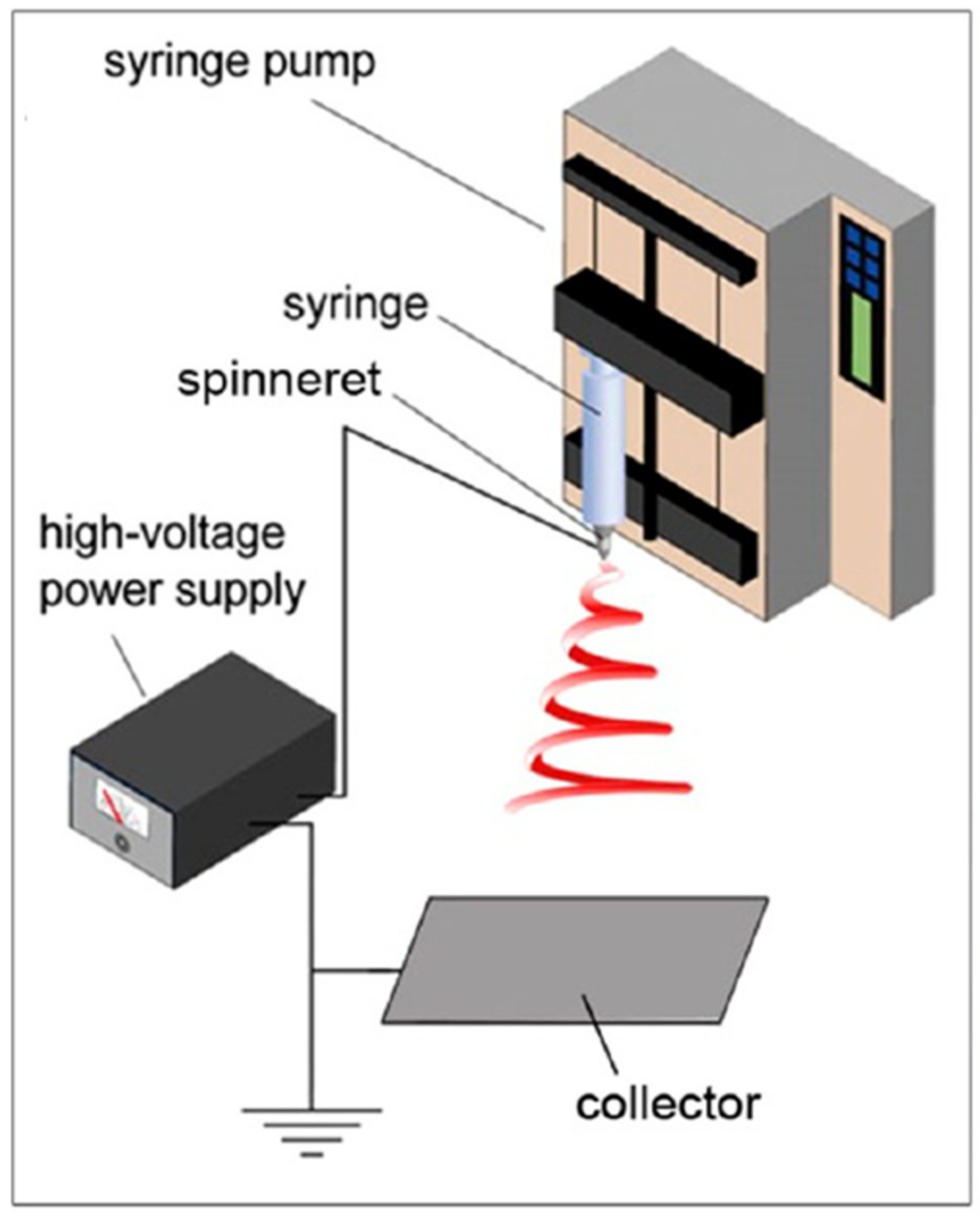
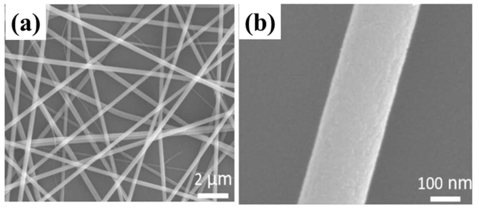
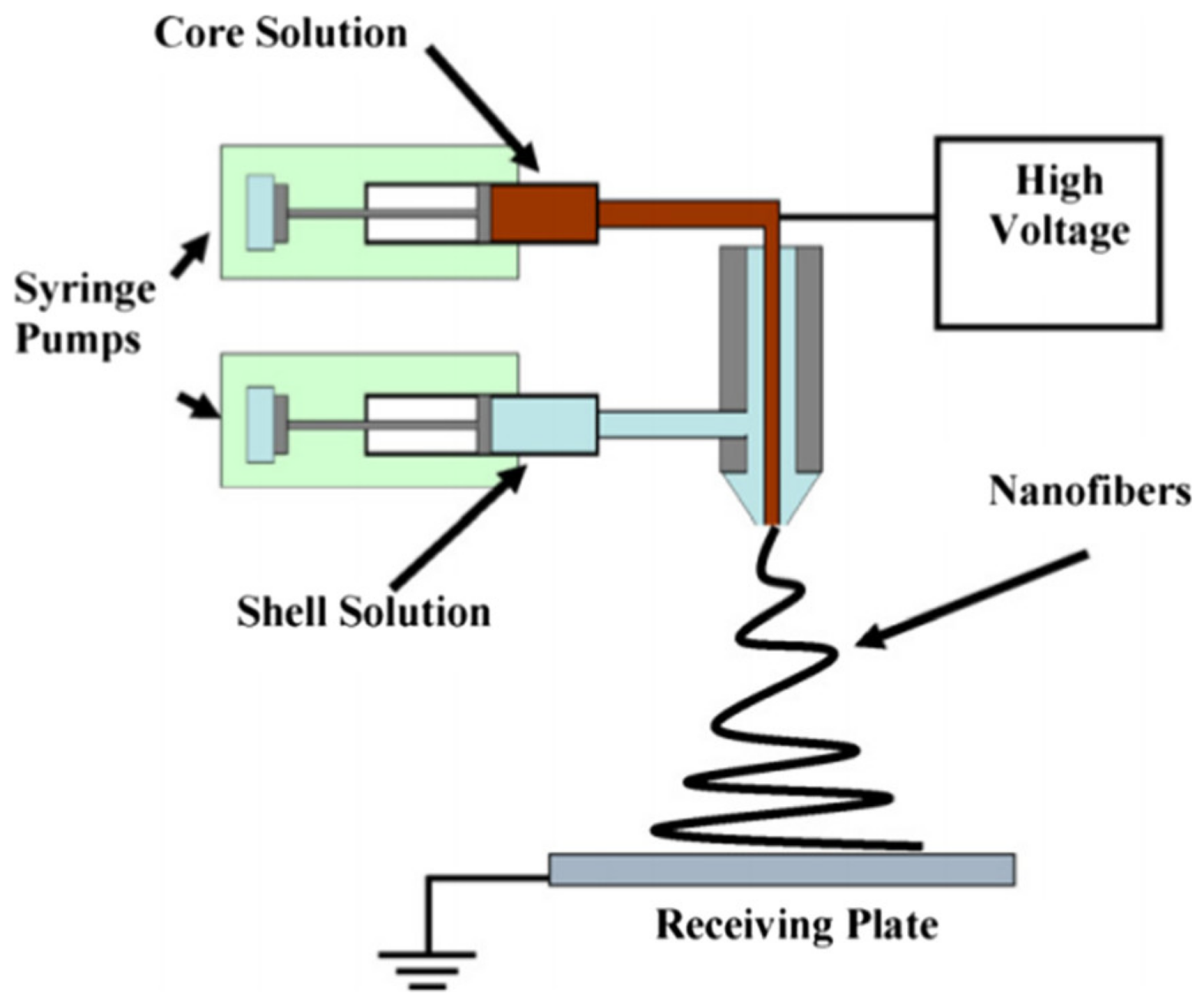
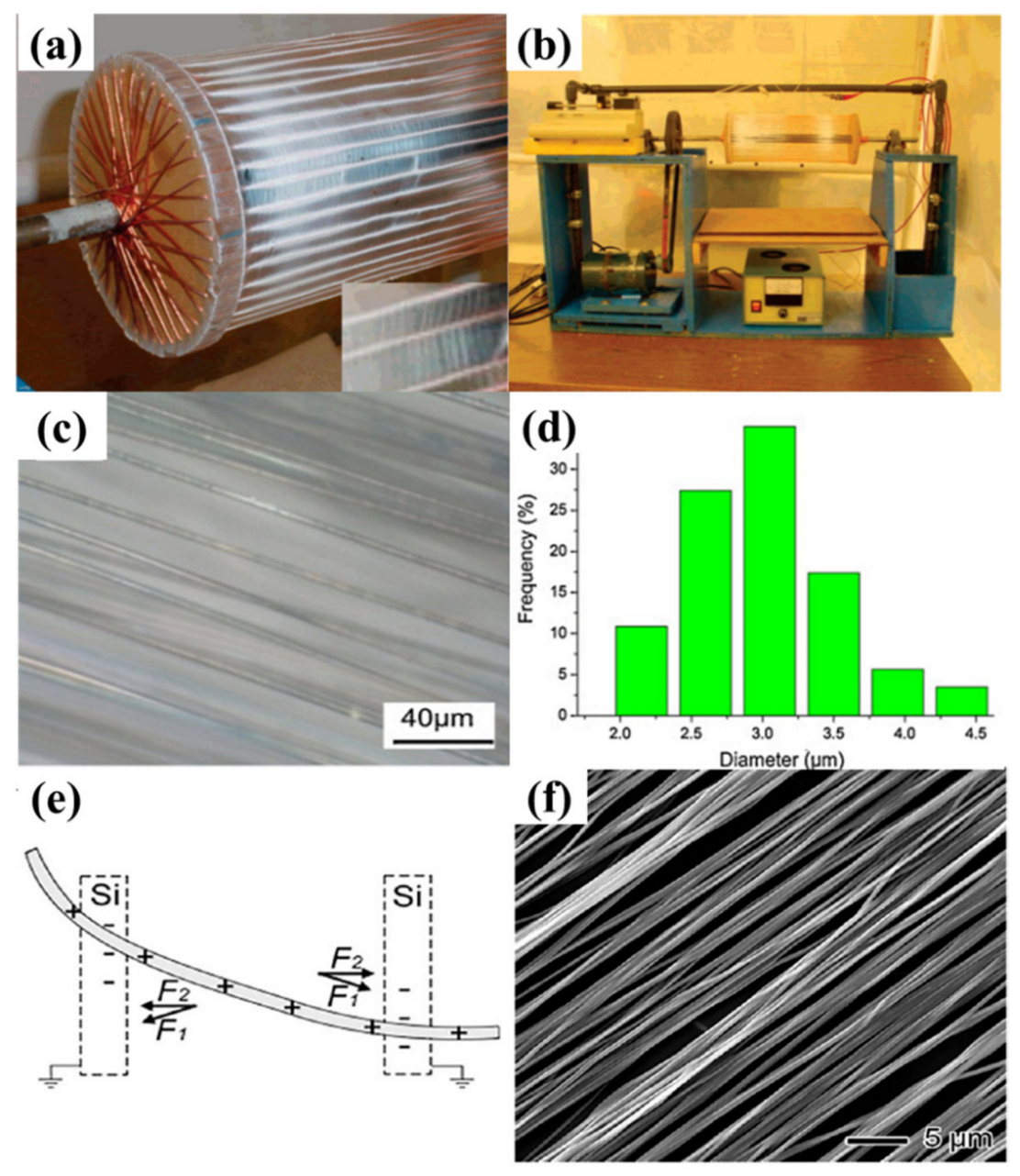
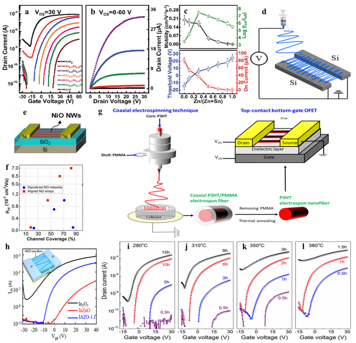
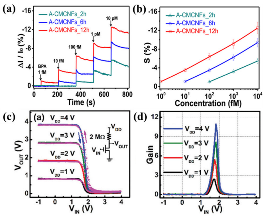
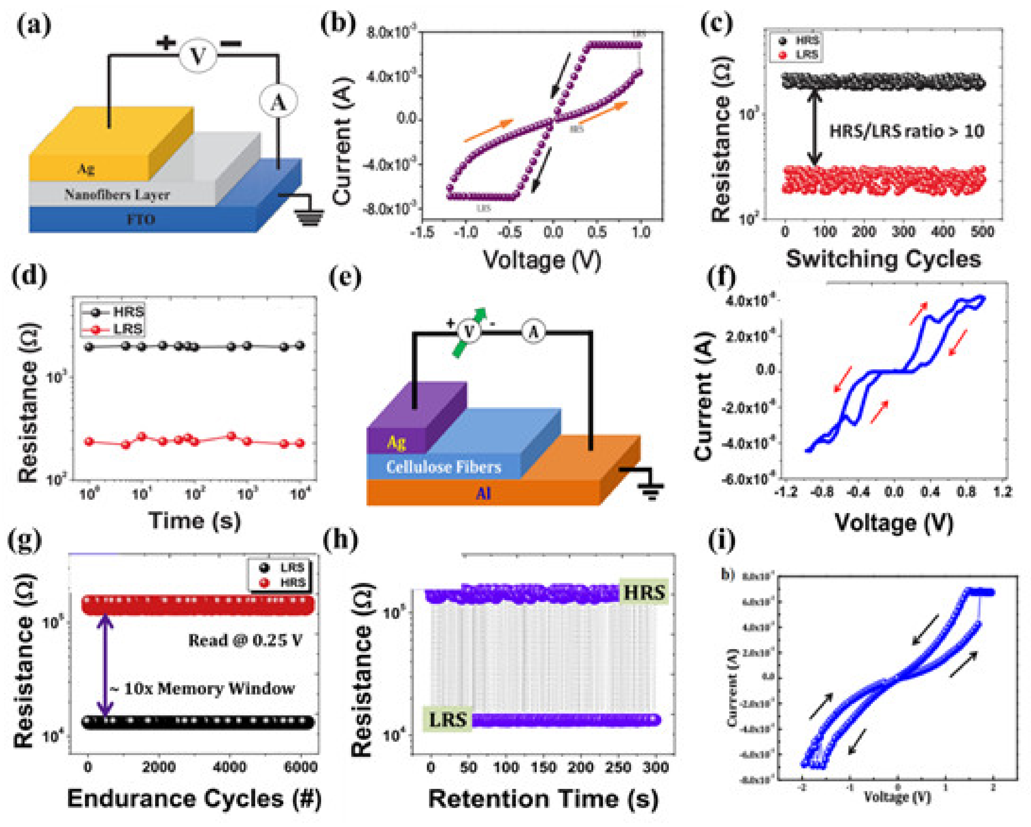
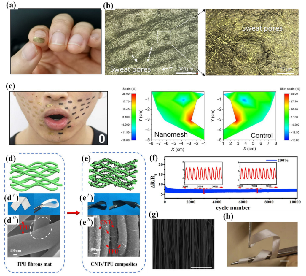
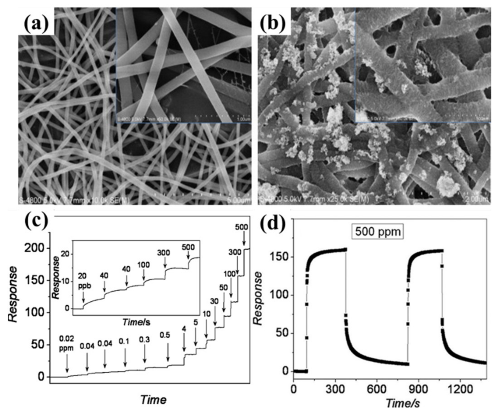
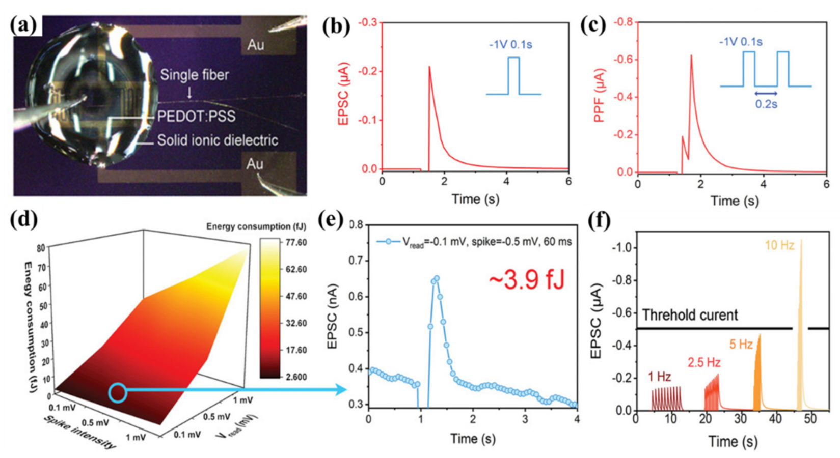
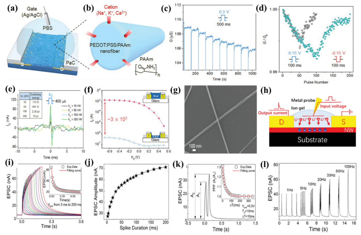
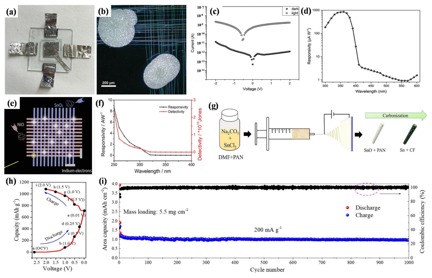
Table 1.
Parameters influencing the nanofibers’ characteristics in the electrospinning process.
| Category | Detailed Factors | Changes in Nanofibers |
|---|---|---|
| Solution Variables | Target material concentration | Fiber diameter increases with the rising concentration |
| Electrical conductivity of the solution | Fiber diameter increases with the rising conductivity. | |
| Viscosity and surface tension of the solution | Too high or too low factors lead to poor fiber morphology. | |
| The molecular weight of the target material | Fiber diameter decreases with increasing molecular weight. | |
| Conditions of Electrospinning Process | Spinneret inner diameter | Fiber size is smaller with a smaller spinneret inner diameter. |
| Flow rate | High flow rate causes increased fiber diameter. | |
| Distance between the needle and the collector | Smaller distance results in larger fiber diameter. | |
| Environmental Factors | Ambient humidity | High humidity prolongs the produced jet. |
| surrounding temperature | Temperature controls the viscosity of the solution and the fiber size. |
Table 2.
Electrical Properties and Applications of FETs with Different Kinds of Nanofibers.
| Year | Nanofiber Material | Mobility (μ, cm2 V−1 s−1) | Ion/Ioff | Characteristics | Applications | References |
|---|---|---|---|---|---|---|
| 2003 | Camphorsulfonic-acid-doped PEO | 1.43 × 10⁻⁴ | — | [61] | ||
| 2005 | RRP3HT | 0.03 | 103 | — | — | [84] |
| 2005 | P3HT | 4 × 10⁻⁴ | 7 | [64] | ||
| 2006 | CuO(p-type) | — | — | Conductivity~3 × 10⁻³ S/cm | — | [67] |
| 2009 | P3HT | 0.017 | 102 | [62] | ||
| 2010 | P3HT | 2 | 105 | Flexible, high frequency operation | [63] | |
| 2010 | MEH-PPV | 10−3 | 780 | Single nanofiber | Photoluminescence/Light-emitting | [82] |
| 2011 | P4TDPP/PMMA | 0.305 | 1.3 × 10⁵ | Crystalline-induced procedure | [85] | |
| 2011 | PANi(p-type) | 2 × 10⁻³ | Single nanofiber | Gas sensor with tunable sensitivity | [80] | |
| 2011 | Au-doped PANi | 11.6 | [65] | |||
| 2012 | P(NDI2OD-T2)/PEO | 0.1 | Single fiber, Stable | [86] | ||
| 2012 | GZO | 104 | Gas sensing including humidity | [81] | ||
| 2013 | ZnO | 4.6 × 10⁻³ | Different calcined atmosphere | [87] | ||
| 2013 | P3HT/PSA | 3.21 × 10⁻² | 104 | Excellent air resistive ability | [69] | |
| 2014 | LiNiO | 3.3 × 10⁻⁴ | Transparent | [88] | ||
| 2014 | P3DT:P3HT | 5.0 × 10⁻³ | High bending stability | [89] | ||
| 2016 | ZnO | 0.018 | 103 | Aligned | Photoconductivity | [90] |
| 2016 | PQT-12/PEO | 1.18 × 10⁻³ | 1.86 × 10³ | Flexible, highly stable under extreme bending conditions | Real-time photosensing | [66] |
| 2016 | MCNFs | High sensitivity, specificity and stability | BPA dection | [83] | ||
| 2016 | AZO | 3.3 × 10⁻³ | 103 | [91] | ||
| 2017 | PEDOT:PSS(p-type) | 5.5 | 730 | [92] | ||
| 2017 | CuO(p-type) | 3.5 | 3 × 10⁵ | Low operating voltage, fast switching speed | Driving unit for LED | [93] |
| 2017 | PS/DPP | 0.22 | 105 | Floating-gate transistor memory | [94] | |
| 2018 | NiO(p-type) | 2.8 | 104 | Excellent dynamic behavior | Light-emitting | [71] |
| 2018 | ZnO | 0.02 | 106 | Low-operating voltages | [78] | |
| 2018 | ZnSnO | 0.17 | 2 × 10⁷ | Low operating voltage | Resistor-loaded inverter | [13] |
| 2018 | InGdO | 17.4 | 108 | Low operating voltage | Resistor-loaded inverter | [95] |
| 2018 | Mg-doped In2O3 | 5.3 | 1.7 × 10⁵ | [73] | ||
| 2019 | Sr-doped In2O3 | 4.8 | 108 | Enhanced stability | Resistor-loaded inverters | [96] |
| 2019 | PEDOT-PSS(p-type) | 0.5 | Non-volatile charge storage | [97] | ||
| 2019 | InZnO | 5.49 | 107 | [68] | ||
| HfInZnO | 0.06 | 105 | ||||
| 2019 | TiO2 | Arranged nanofibers, Mixed anatase-rutile TiO2 | [98] | |||
| 2019 | P3HT | 0.357 | 4.57 × 10³ | Hollow (Coaxial electrospinning) | [70] | |
| 2020 | In2O3 | 1.27 | 5 × 10⁷ | Excellent reliability and reproducibility | [99] | |
| 2020 | In2O3 | 1.53 | 8 × 10⁴ | Nontoxic and low-temperature preparation | [76] | |
| 2020 | ZnSnO | 21.58 | 108 | Different annealing atmosphere and temperature | Resistor-loaded inverters | [74] |
| 2020 | IGO | 35.1 | 107 | Dual-gate structure | [100] | |
| 2020 | InYbO | 6.18 | 107 | Outstanding selectivity towards DMF | Gas sensing | [101] |
| 2020 | Al, Ga, Cr doped In2O3 | 2.0 | 108 | Low operating voltage | Resistor loaded inverter | [72] |
| 2020 | Al functionalized β-Bi2O3 | 64.4 | 106 | Excellent sensitivity, stability and reproducibility | Biosensor for detection of serotonin | [102] |
| 2020 | IGZO | 5.32 | 4.35 × 10⁶ | Good electrical properties and reliability | Resistor-loaded inverters | [79] |
| 2021 | IGZO | 2.45 | 3.8 × 10² | Double gate, high pH sensitivities | Chemical sensors | [103] |
| 2021 | In2O3 | 1.51 | 1.5 × 10⁷ | Ar/O2 plasma treatment | [104] | |
| 2021 | IAZO | 30 | 5.6 × 10⁶ | [75] | ||
| 2021 | In2O3 | 27.7 | 107 | Great stability | Resistor-loaded inverter | [105] |
| 2021 | SnO2 | 2.3 | 106 | Adjustable grain size | [77] | |
| 2021 | PVA (with evaporated CuPc) | 8.77 × 10⁻³ | 1.37 × 10³ | Short response and recovery time for detecting NO2 | Gas monitoring | [106] |
Publisher’s Note: MDPI stays neutral with regard to jurisdictional claims in published maps and institutional affiliations. |
© 2022 by the authors. Licensee MDPI, Basel, Switzerland. This article is an open access article distributed under the terms and conditions of the Creative Commons Attribution (CC BY) license (https://creativecommons.org/licenses/by/4.0/).
Share and Cite
MDPI and ACS Style
Guo, Y.; Qiao, Y.; Cui, T.; Wu, F.; Ji, S.; Yang, Y.; Tian, H.; Ren, T. Electrospun Nanofibers for Integrated Sensing, Storage, and Computing Applications. Appl. Sci. 2022, 12, 4370. https://0-doi-org.brum.beds.ac.uk/10.3390/app12094370
AMA Style
Guo Y, Qiao Y, Cui T, Wu F, Ji S, Yang Y, Tian H, Ren T. Electrospun Nanofibers for Integrated Sensing, Storage, and Computing Applications. Applied Sciences. 2022; 12(9):4370. https://0-doi-org.brum.beds.ac.uk/10.3390/app12094370
Chicago/Turabian StyleGuo, Yizhe, Yancong Qiao, Tianrui Cui, Fan Wu, Shourui Ji, Yi Yang, He Tian, and Tianling Ren. 2022. "Electrospun Nanofibers for Integrated Sensing, Storage, and Computing Applications" Applied Sciences 12, no. 9: 4370. https://0-doi-org.brum.beds.ac.uk/10.3390/app12094370
Note that from the first issue of 2016, this journal uses article numbers instead of page numbers. See further details here.