Article

Electronic Band Structure of Transition Metal Dichalcogenides from Ab Initio and Slater–Koster Tight-Binding Model

by
Jose Ángel Silva-Guillén
1,
Pablo San-Jose
2 and
Rafael Roldán
2,*
1
Fundación IMDEA Nanociencia, C/Faraday 9, Campus Cantoblanco, Madrid 28049, Spain
2
Instituto de Ciencia de Materiales de Madrid, ICMM-CSIC, Sor Juana Ines de la Cruz 3, Madrid 28049, Spain
*
Author to whom correspondence should be addressed.
Submission received: 19 July 2016 / Revised: 14 September 2016 / Accepted: 20 September 2016 / Published: 1 October 2016
(This article belongs to the Special Issue Two-Dimensional Transition Metal Dichalcogenides)

Abstract

:
Semiconducting transition metal dichalcogenides present a complex electronic band structure with a rich orbital contribution to their valence and conduction bands. The possibility to consider the electronic states from a tight-binding model is highly useful for the calculation of many physical properties, for which first principle calculations are more demanding in computational terms when having a large number of atoms. Here, we present a set of Slater–Koster parameters for a tight-binding model that accurately reproduce the structure and the orbital character of the valence and conduction bands of single layer MX 2 , where M = Mo, W and X = S, Se. The fit of the analytical tight-binding Hamiltonian is done based on band structure from ab initio calculations. The model is used to calculate the optical conductivity of the different compounds from the Kubo formula.

1. Introduction

Soon after the discovery of graphene by mechanical exfoliation, this technique was applied to the isolation of other families of van der Waals materials [1]. Among them, semiconducting transition metal dichalcogenides (TMD) are of special interest because they have a gap in the optical range of the energy spectrum, which is what makes them candidates for applications in photonics and optoelectronics [2,3,4]. The electronic properties of these materials are highly sensitive to external conditions such as strain, pressure or temperature. For instance, a direct-to-indirect gap and even a semiconducting-to-metal transition can be induced under specific conditions [5,6,7,8,9,10]. They also present a strong spin–orbit coupling (SOC) that, due to the absence of inversion symmetry in single layer samples, lifts the spin degeneracy of the energy bands [11]. In time reversal–symmetric situations, inequivalent valleys have opposite spin splitting, leading to the so called spin–valley coupling [12,13,14], which has been observed experimentally [15,16,17,18,19,20]. The coupling of the spin and valley degrees of freedom in semiconducting TMDs creates the possibility to manipulate them for future applications in spintronics and valleytronics nanodevices [15,21,22,23,24].
On the other hand, TMDs present a high stretchability. Moreover, external strain can be used to efficiently manipulate their electronic and optical properties [25]. Non-uniform strain profiles can be used to create funnels of excitons, which allows for capturing a broad light spectrum, concentrating carriers in specific regions of the samples [5,26]. Strain engineering can be also used to exploit the piezoelectric properties of atomically thin layers of TMDs, converting mechanical to electrical energy [27].
The rich orbital structure of the valence and conduction bands of semiconducting TMDs [28] complicates the construction of a tight-binding (TB) model for these systems. Such a TB model must be precise enough as to include all the pertinent orbitals of the relevant bands, but at the same time, simple enough as to be used without too much effort in calculations of optical and transport properties of these materials. The advantage of a tight-binding description with respect to first-principles methods is that it provides a simple starting point for the further inclusion of many-body electron–electron interaction, external strains, as well as of the dynamical effects of the electron–lattice interaction. Tight-binding approaches are often more convenient than ab initio methods for investigating systems involving a very large number of atoms [26], disordered and inhomogeneous samples [29], strained and/or bent samples [30,31], materials nanostructured in large scales (nanoribbons [32,33], ripples [34]) or in twisted multilayer materials. The aim of the present paper is twofold. Starting from the TB model for MoS 2 developed by Cappelluti et al. [35], we present a more accurate set of Slater–Koster parameters obtained from a more sophisticated fitting procedure, and we further generalize it to the other families of semiconducting TMDs, namely WS 2 , MoSe 2 and WSe 2 . Finally, we apply the obtained tight-binding models to calculate the optical conductivity of the four compounds.

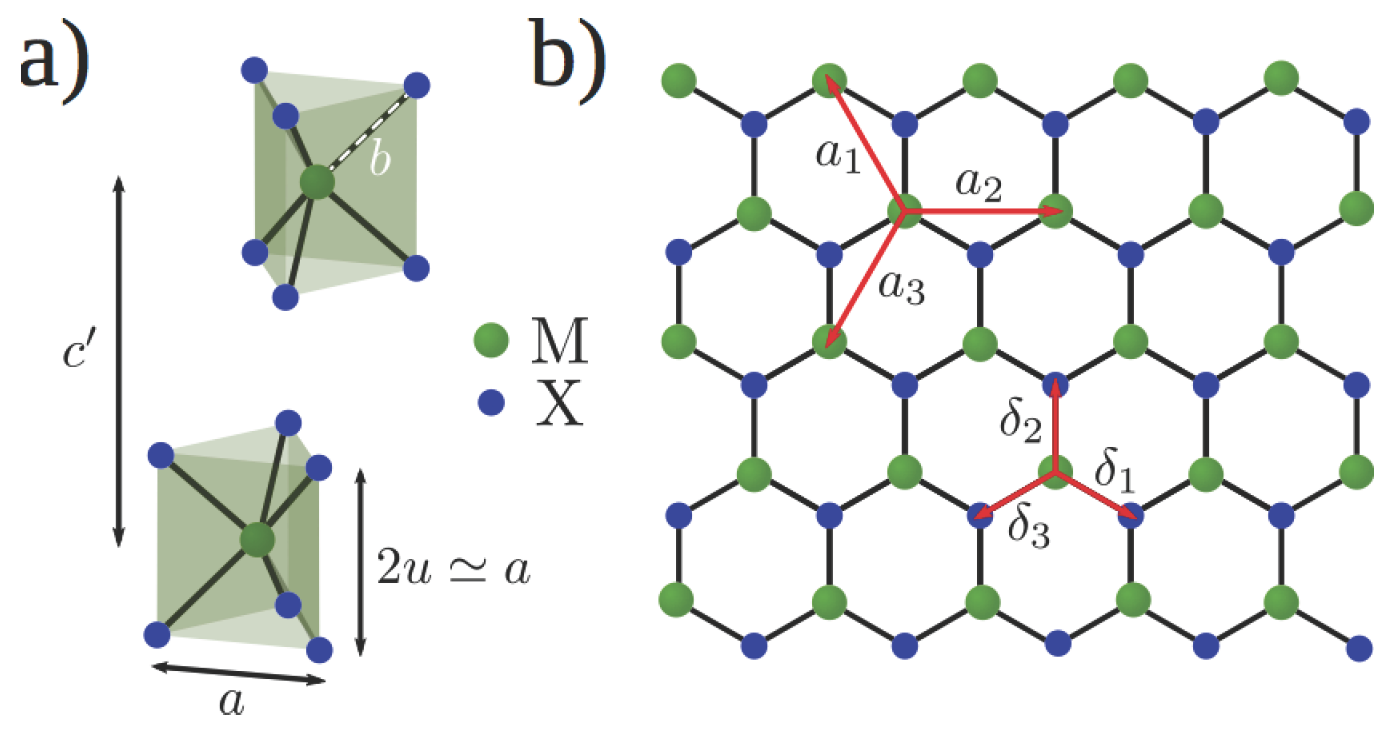
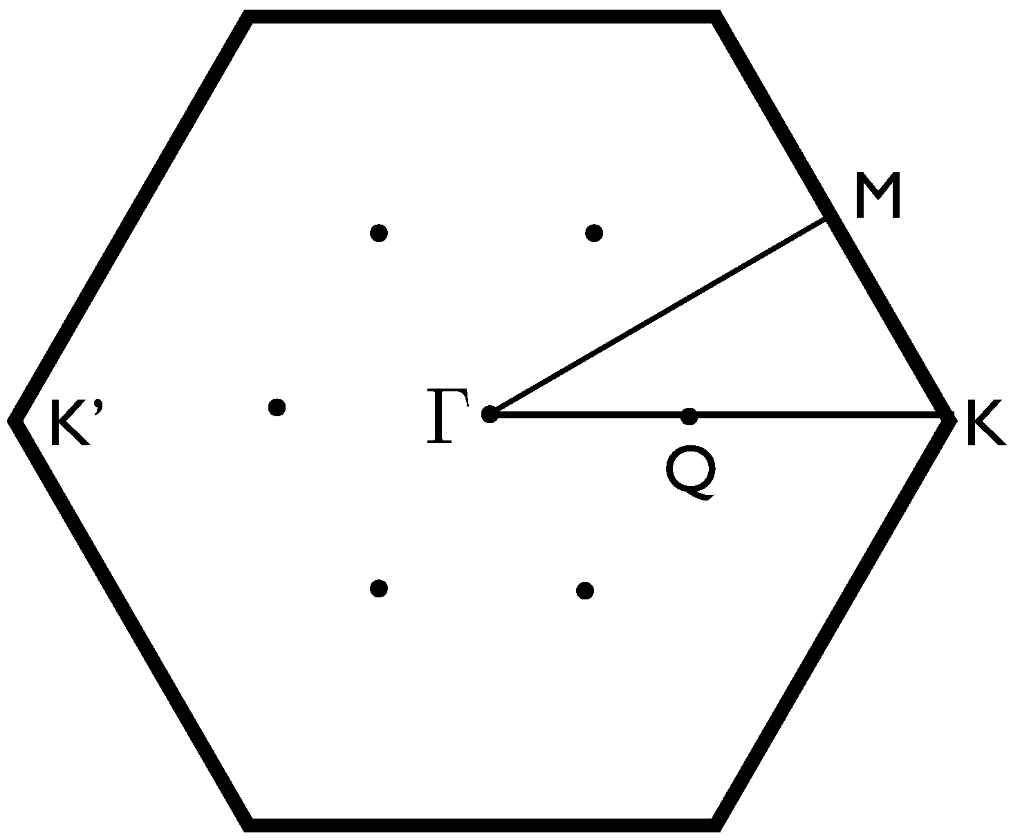
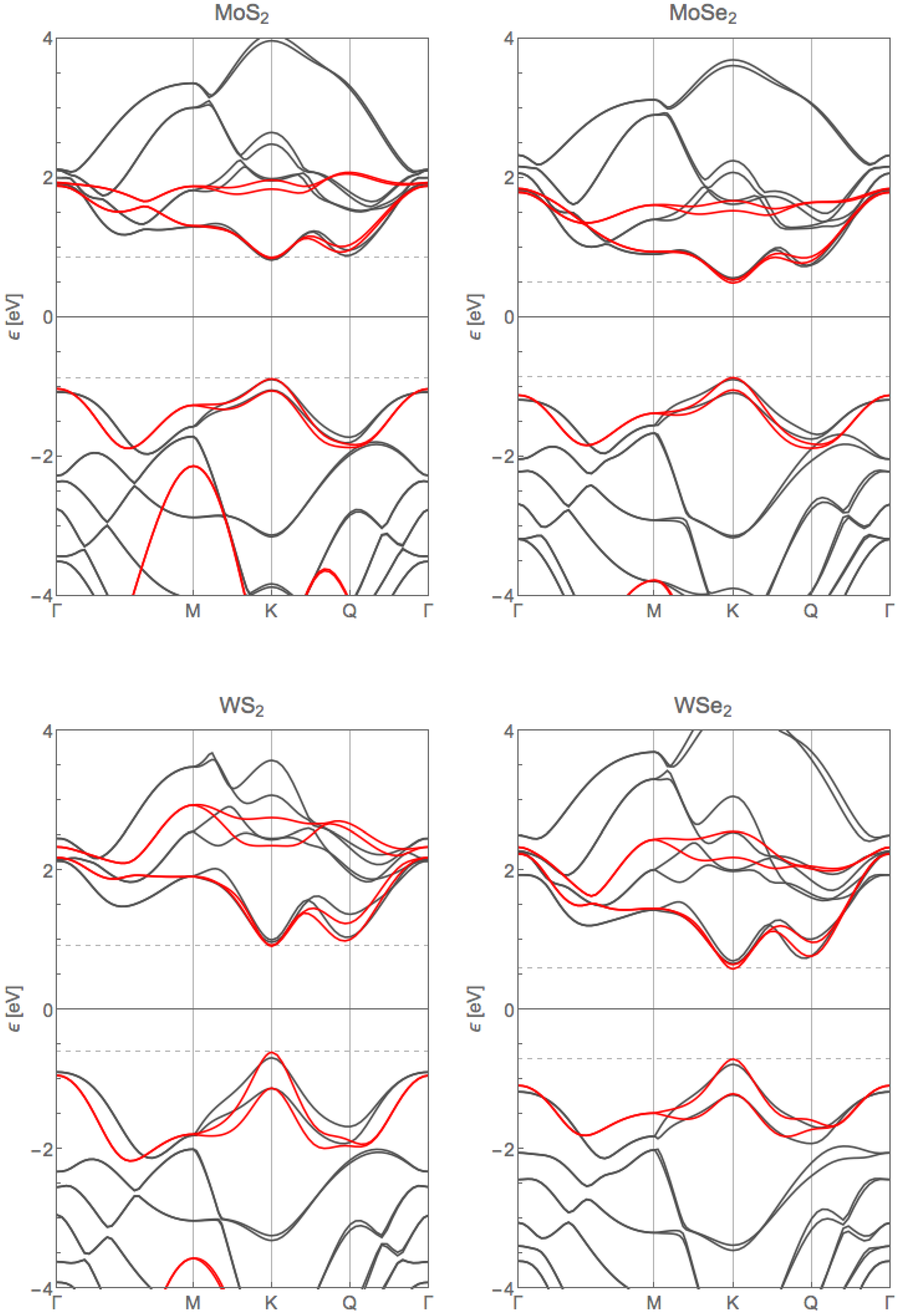
2. Electronic Band Structure

The crystal structure of MX 2 is schematically shown in Figure 1. A single layer is composed by an inner layer of metal M atoms ordered on a triangular lattice, which is sandwiched between two layers of chalcogen X atoms placed on the triangular lattice of alternating hollow sites. We use a notation such that a corresponds to the distance between nearest neighbor in-plane MM and XX atoms, b is the nearest neighbor MX separation and u is the distance between the M and X planes. The MX 2 crystal forms an almost perfect trigonal prism structure with b 7 / 12 a and u a / 2 . The lattice parameters of the bulk compounds corresponding to the more commonly studied TMDs are given in Table 1 [36,37,38]. The in-plane Brillouin zone is a hexagon, and it is shown in Figure 2. It contains the high-symmetry points Γ = ( 0 , 0 ) , K = 4 π / 3 a ( 1 , 0 ) and M = 4 π / 3 a ( 0 , 3 / 2 ) . The six Q points correspond to the approximate position of a local minimum of the conduction band.
In order to study the electronic band structure of single-layer TMDs, we use the Density Functional Theory (DFT) calculations presented by some of the authors in Reference [28], in which the intrinsic spin–orbit interaction term for all atoms is included. Figure 3 shows the band structures for single-layer M X 2 (black lines) together with the TB bands that will be discussed later (red lines) (DFT calculations were done using the Siesta code [39,40], with the exchange–correlation potential of Ceperly–Alder [41] as parametrized by Perdew and Zunger [42]. A split-valence double- ζ basis set including polarization functions was considered [43]. The energy cutoff and the BZ sampling were chosen to converge the total energy with a value of 300 Ry and 30 × 30 × 1 . The energy cutoff was set to 10 - 6 eV. Spin-orbit interaction of the different compounds was considered by following the method developed in Reference [44]. The lattice parameters used in the calculation are set to their experimental values [45,46,47] and are given in Table 1). One of the main characteristics of TMDs is that, contrary to what happens in other 2D crystals like graphene or phosphorene, the valence and conduction bands of M X 2 present a very rich orbital contribution. As explained in detail in Reference [35], they are made by hybridization of the d orbitals of the transition metal, and the p orbitals of the chalcogen. More specifically, the analysis of the orbital content of the set of bands containing the first four conduction bands and the first seven valence bands, which cover an energy window from −7 to 5 eV around the Fermi level, approximately, reveals that these bands are dominated by the five 4d (5d) orbitals of the metal Mo (W) and the six (three for each layer) 3p (4p) orbitals of the chalcogen S (Se), totaling to up to 93% of the total orbital weight [35].
Single-layer TMDs are direct gap semiconductors, with the gap located at the two inequivalent K and K’ points of the Brillouin zone (Figure 3). The main orbital character at the edge of the valence band is due to a combination of d x 2 - y 2 and d x y orbitals of the metal M, which hybridize with p x and p y orbitals of the chalcogen X. On the other hand, the edge of the conduction band is formed by d 3 z 2 - r 2 orbital of M, plus some contribution of p x and p y orbitals of X [35]. Contrary to single-layer samples, multi-layer compounds are indirect gap semiconductors. The edge of the valence band lies at the Γ point of the BZ, having a major contribution from d 3 z 2 - r 2 and p z orbitals of M and X atoms, respectively. The edge of the conduction band in multi-layer samples is placed at the Q point of the BZ. It is important to notice that the Q point is not a high symmetry point of the Brillouin zone, and therefore its exact position depends on the number of layers and on the specific compound. The orbital character at the Q point originates mainly from the d x y and d x 2 - y 2 orbitals of the metal M, plus p x and p y orbitals of the chalcogen X, plus a non negligible contribution of p z and d 3 z 2 - r 2 of X and M atoms, respectively. Figure 4 and Figure 5 and Figure B1, Figure B2 and Figure B3 represent these relative orbital weights in detail for the different compounds. The extremely rich orbital contribution to the relevant bands that occur in semiconducting TMDs complicates the derivation of a minimal TB model, valid in the whole Brillouin zone. Another important feature of TMDs is that they present a strong SOC, which leads to a large splitting of the valence band at the K and K’ points of the BZ (see Figure 3). The splitting is bigger for W than for Mo compounds, due to the heavier mass of the former. SOC also leads to a splitting of the conduction band at the K point, as well as at the minimum at the Q point [37,48].

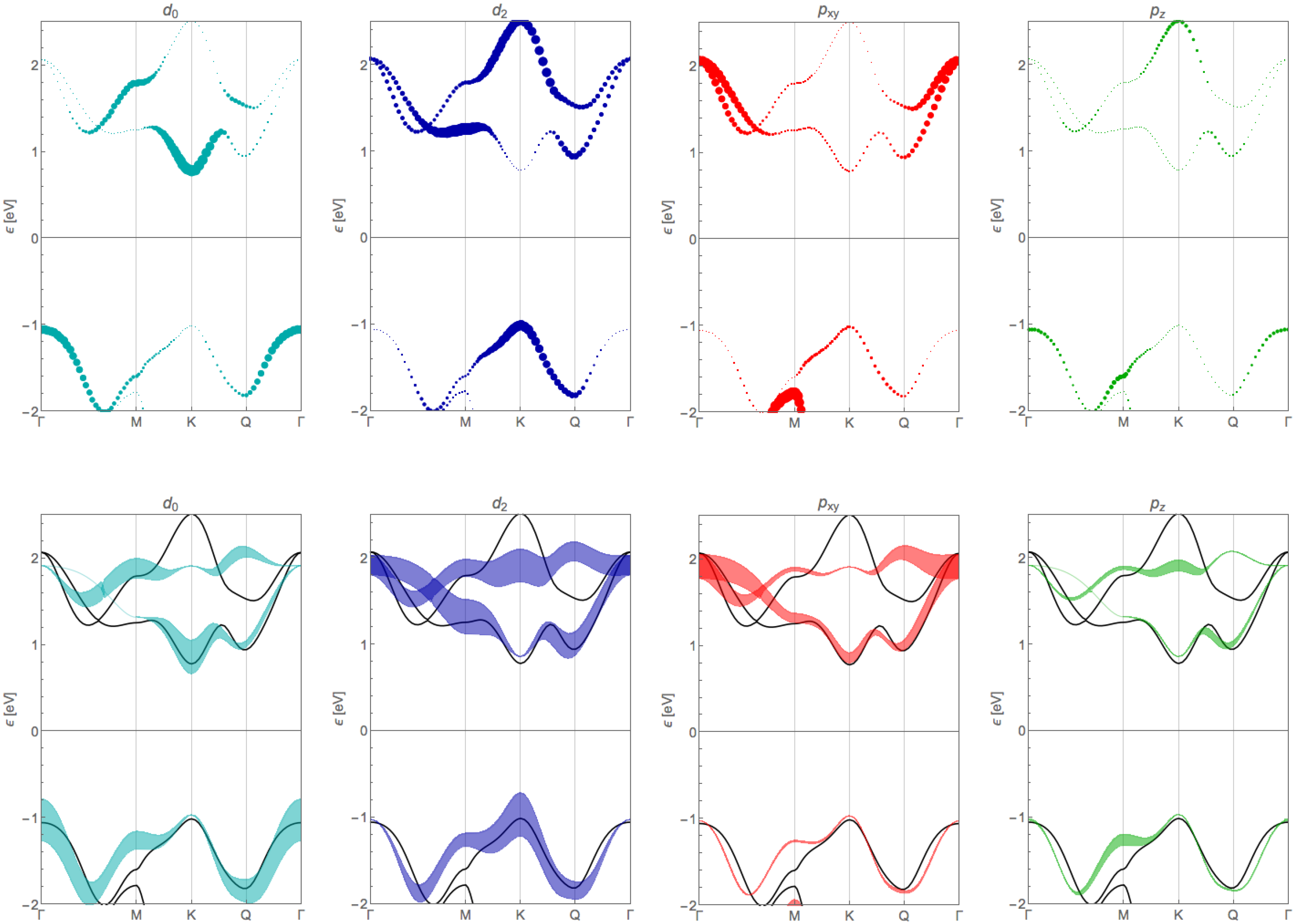
3. Tight-Binding Model

In this section, we consider the electronic band structure of TMDs, in the whole BZ, from a Slater–Koster tight-binding approximation [49]. We use the model developed by Cappelluti et al. [35], which contains 11 orbitals per layer. In particular, the model contains the five d orbitals of the metal M atom and the six p orbitals of the two chalcogen X atoms in the unit cell. The used scheme has been recently used in other works studying the electronic band structure of TMDs from a tight-binding perspective [50,51]. The corresponding base can be expressed as [35]
p x t , p y t , p z t , d 3 z 2 - r 2 , d x z , d y z , d x 2 - y 2 , d x y , p x b , p y b , p z b ,
where the indices t and b label the top and bottom chalcogen planes, respectively. The model is defined by the hopping integrals between the different orbitals, which are described in terms of σ , π and δ ligands. In the following, we reproduce the most important results, and we refer the reader to Reference [35,48] for details of the model. The Slater–Koster parameters that account for the relevant hopping processes of the model are V p d σ and V p d π for MX bonds, V d d σ , V d d π and V d d δ for MM bonds, and V p p σ and V p p π for XX bonds. Additional parameters of the theory are the crystal fields Δ 0 , Δ 1 , Δ 2 , Δ p , Δ z , describing, respectively, the atomic level of the l = 0 ( d 3 z 2 - r 2 ), the l = 1 ( d x z , d y z ), the l = 2 ( d x 2 - y 2 , d x y ) M orbitals, the in-plane ( p x , p y ) X orbitals and the out-of-plane p z X orbitals.
This model can be simplified by performing a unitary transformation that takes the p orbitals of the top and bottom layers of the X atoms into their symmetric and antisymmetric combinations with respect to the z-axis. This way, the 11-band model is decoupled into a 6 × 6 block with even (odd) symmetry of the p x , p y ( p z ) orbitals with respect to z - z inversion, and a 5 × 5 band block with opposite combination. Since low energy excitations belong exclusively to the first block, the fit to DFT that we will present later will be performed within this sector. Therefore, the relevant bands above and below the gap are well accounted for by the reduced Hilbert space:
ψ = d 3 z 2 - r 2 , d x 2 - y 2 , d x y , p x S , p y S , p z A ,
where the S and A superscripts stand for the symmetric and antisymmetric combinations of the p-orbitals of the X atom, p i S = 1 / 2 ( p i t + p i b ) and p i A = 1 / 2 ( p i t - p i b ) , with i = x , y , z . The tight-binding Hamiltonian defined by base (2), including local spin–orbit coupling, can be expressed in real space as
H = i , μ ν ϵ μ , ν c i , μ c i , ν + i j , μ ν [ t i j , μ ν c i , μ c j , ν + H . c . ] ,
where c i , μ ( c i , μ ) creates (annihilates) an electron in the unit cell i in the atomic orbital μ = 1 , , 6 , belonging to the Hilbert space defined by base (2). The Hamiltonian in k-space can be expressed as [30,35,48]:
H = H M M H M X H M X H X X , H M M = ϵ M + 2 i = 1 , 2 , 3 t i M M cos k · a i , H X X = ϵ X + 2 i = 1 , 2 , 3 t i X X cos k · a i , H M X = i = 1 , 2 , 3 t i M X e - i k · δ i ,
where the vectors ( δ i ) and ( a i ) are shown in Figure 1b. The analytical expressions for the TB model are given in Appendix A.

4. Slater–Koster Parameters from Fitting to Ab Initio Calculations

Finding the optimal set of Slater–Koster parameters for the TB model considered here is a difficult task. Two main requirements must be satisfied: a good reproduction of the structure of the relevant electronic bands, and faithful representation of the orbital contribution along such bands. The last condition is especially relevant because, for example, different kinds of strains do not affect all the hoppings in the same manner. Therefore, capturing the proper orbital contribution is essential when using the TB model for calculations of physical properties of strained membranes. The same happens when one considers the effect of vacancies, adatoms, etc.
In this work, we have obtained the Slater–Koster parameters for each compound from a minimization procedure that has the possibility to consider a band/momentum resolved weight that allows us to resolve more accurately particular k regions of selected bands (e.g., edges of the valence and conduction bands)(The calculation of tight-binding band structure and fitting to DFT have been performed using the MathQ package, developed by P. San-Jose. (Source: http://www.icmm.csic.es/sanjose/MathQ/MathQ.html)). Furthermore, we can apply constrictions for the orbital contribution at specific band regions, taking as a reference the information from the DFT wave-functions. The sets of Slater–Koster parameters that we have obtained for the four compounds are given in Table 2. During the fitting, we have used only the 6 × 6 block of the Hamiltonian because, as explained above, it accounts for the valence and conduction bands. Therefore, we obtain as output all the Slater–Koster parameters but one, Δ 1 , which is the crystal field corresponding to d 2 = d x z , y z orbitals, whose contribution is absent in the 6 × 6 block. What we have done to estimate the value of Δ 1 is to impose that the edges of the TB and DFT bands coincide for the lower energy band of the 5 × 5 block at the K point of the Brillouin zone. The band structure calculated with the 6 × 6 block of this model is plotted in Figure 3, as compared to DFT calculations. In Figure 4 and Figure 5 and Figure B1, Figure B2 and Figure B3, we compare the orbital contribution of the TB model, using the Slater–Koster parameters of Table 2, to the corresponding orbital contribution as obtained from DFT. We show the results for the most relevant orbitals ( d 0 = d 3 z 2 - r 2 , d 2 = d x y , d x 2 - y 2 , p x y = p x , p y and p z ), and we can conclude that the TB model not only presents an acceptable fit to the band structure, but, importantly, the wave-functions also reproduce the DFT orbital contribution at the most important points of the band structure. Table 3 contains the main orbital contribution of each compound at the most relevant edges of the band structure, namely valence and conduction bands at K point, and valence band at Γ point of the Brillouin zone. We notice that the main restriction of the TB model considered here is that it only includes up to next-nearest-neighbor hopping terms, and this is why the fit to the DFT bands cannot be perfect. More sophisticated methods such as DFT based tight-binding Hamiltonians represented in the basis of maximally localized Wannier functions can lead to better agreements, at the cost of inclusion of longer-range hopping terms [52]. For the case presented here, and due to the automatised fitting procedure, we can conclude that the set of parameters presented in Table 2 must be close to the ideal solution.

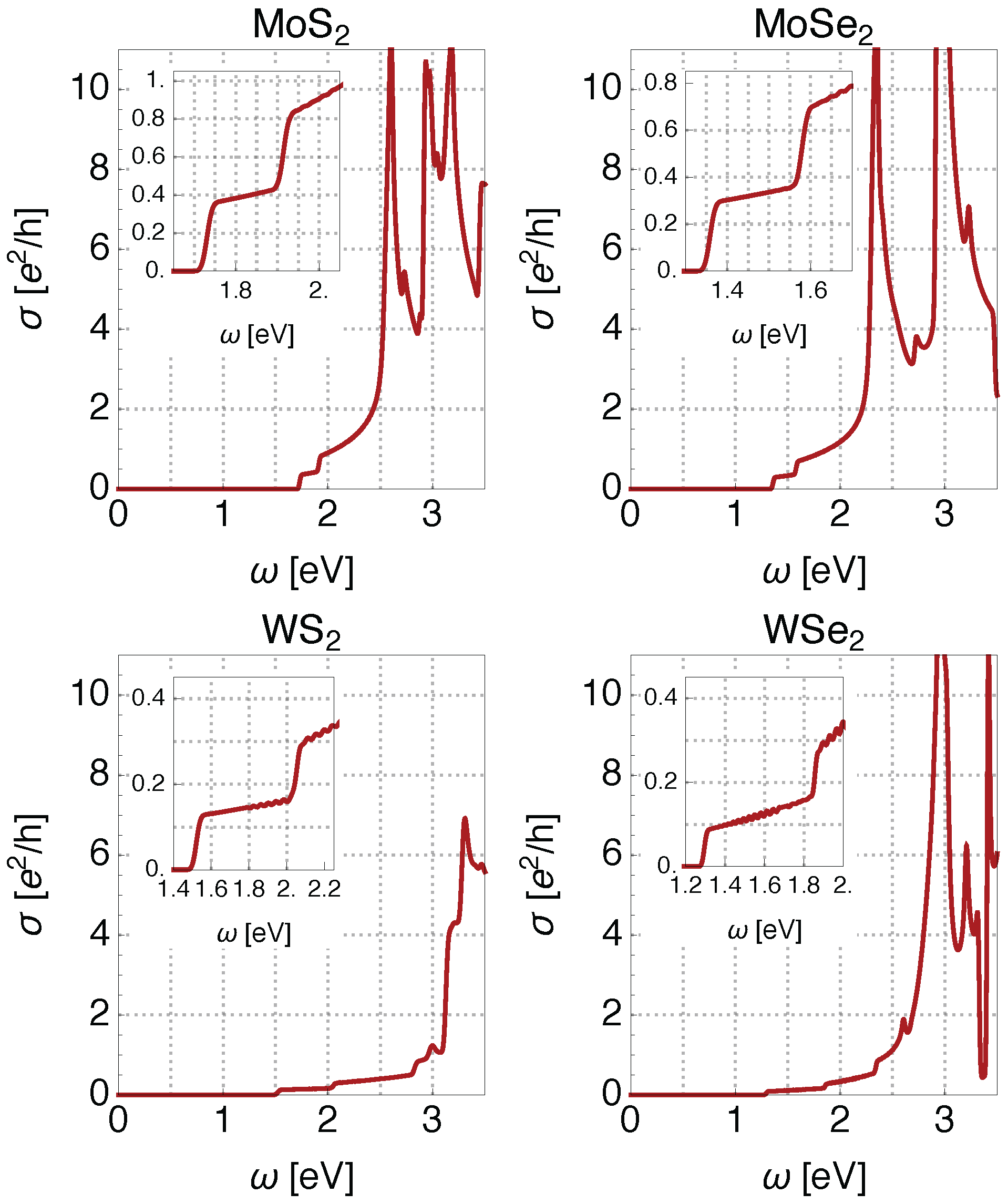
5. Optical Conductivity

Once we have the tight-binding models for the four compounds, we can use them to calculate physical observables as, for example, the optical conductivity σ ( ω ) . For this aim, we use the Kubo formula
σ ( ω ) = e 2 h A ω m n , k ( f ( E n ) - f ( E m ) ) × Ψ n ( k ) | v ^ | Ψ m ( k ) 2 δ [ ω - ( E n ( k ) - E m ( k ) ) ] ,
where A is the area of the unit cell, Ψ n ( k ) is the eigenstate of energy E n , f ( E n ) = 1 / ( 1 + e β E n ) is the Fermi–Dirac distribution function, in terms of the inverse temperature β = 1 / k B T and considering that the Fermi energy lies in the gap, and v ^ = ( 1 / ) H ^ / k is the velocity operator. The results are shown, for the approximate range of validity of our TB models (∼1 eV above and below the band gap), in Figure 5. We observe that, for all the compounds, there is a threshold for the onset of optical transitions that is equal to the gap Δ. The steplike structure of σ ( ω ) at low energies (see insets of each panel in Figure 5) is due to the SOC, which leads to two sets of optical transitions in the spectrum. Due to the stronger SOC of heavier W atoms, the effect is especially visible in WS 2 and WSe 2 , with plateaus of ∼0.4 eV in σ ( ω ) , corresponding to the energy splitting of the valence band at the K and K’ points of the Brillouin zone (see Figure 3). These transitions lead to the well-known A and B absorption peaks observed in photoluminescence [16]. We further notice that our results for the optical conductivity are in good agreement, even for the onset energy, with experimental measurements (see e.g., Reference [53]). At higher energies, the optical conductivity shows a series of peaks that are associated with optical transitions between flat bands in the spectrum (van Hove singularities). Such van Hove singularities are clearly evident for the valence and conduction bands at the M point of the Brillouin zone (see Figure 3). We notice that disorder (vacancies, adatoms, etc.), not included here, can lead to the creation of midgap states that allow for additional optical transitions in the spectrum [29].

6. Conclusions

In summary, we have generalized the tight-binding model for MoS 2 of Reference [35] to the other families of semiconducting TMDs: MoSe 2 , WS 2 and WSe 2 . Our main result is the set of Slater–Koster parameters of Table 2, which have been obtained from a fit to DFT calculations in which special care was paid to capture the main orbital contribution of the TB bands at the relevant regions of the band structure. The obtained models have been used to calculate the optical conductivity of the different compounds. This approximation can be straightforwardly generalized to multi-layer systems with arbitrary stacking orders, heterostructures made from the stacking of layers of different compounds, twisted multilayers, strained and/or disordered samples, etc.

Acknowledgments

We appreciate useful conversations with Emmanuele Cappelluti, Pablo Ordejón, Francisco Guinea, María Pilar López-Sancho and Habib Rostami. Jose Angel Silva-Guillén acknowledges financial support from European Union’s Seventh Framework Programme (FP7/2007–2013) through the ERC Advanced Grant NOV- GRAPHENE (GA 290846). Pablo San-Jose was supported by MINECO through Grant No. FIS2015-65706-P and the Ramón y Cajal programme RYC-2013-14645. Rafael Roldán acknowledges financial support from MINECO (FIS2014-58445-JIN).

Author Contributions

J.S.-G. performed the ab-initio calculations. P.S.-J. calculated the conductance curves. R.R. devised the project, performed the tight-binding fits and wrote the manuscript. All authors contributed to discussions.

Conflicts of Interest

The authors declare no conflict of interest.

Appendix A. On-Site and Hopping Matrices of the 6×6 Block

For convenience, we reproduce in this appendix the analytical expressions for the model. The on-site terms of the Hamiltonian can be written in the compact form [48]:
ϵ = ϵ M 0 0 ϵ X ,
where
ϵ M = Δ 0 0 0 0 Δ 2 - i λ M s ^ z 0 i λ M s ^ z Δ 2 , ϵ X = Δ p + t x x - i λ X 2 s ^ z 0 i λ X 2 s ^ z Δ p + t y y 0 0 0 Δ z - t z z ,
where λ M and λ X are the SOC of the metal (M) and chalcogen atoms (X), respectively, and s ^ z = ± is the z-component of the spin degree of freedom [48]. The effects of vertical hopping V p p between top and bottom X atoms are considered through the terms t x x = t y y = V p p π , and t z z = V p p σ . The nearest-neighbor hopping between M and X atoms are
t 1 M X = 2 7 7 - 9 V p d π + 3 V p d σ 3 3 V p d π - V p d σ 12 V p d π + 3 V p d σ 5 3 V p d π + 3 V p d σ 9 V p d π - 3 V p d σ - 2 3 V p d π + 3 V p d σ - V p d π - 3 3 V p d σ 5 3 V p d π + 3 V p d σ 6 V p d π - 3 3 V p d σ ,
t 2 M X = 2 7 7 0 - 6 3 V p d π + 2 V p d σ 12 V p d π + 3 V p d σ 0 - 6 V p d π - 4 3 V p d σ 4 3 V p d π - 6 V p d σ 14 V p d π 0 0 ,
t 3 M X = 2 7 7 9 V p d π - 3 V p d σ 3 3 V p d π - V p d σ 12 V p d π + 3 V p d σ - 5 3 V p d π - 3 V p d σ 9 V p d π - 3 V p d σ - 2 3 V p d π + 3 V p d σ - V p d π - 3 3 V p d σ - 5 3 V p d π - 3 V p d σ - 6 V p d π + 3 3 V p d σ ,
where the direction of the hopping labelled by subindices 1, 2, and 3 is shown in Figure 1b. Hopping terms corresponding to processes between the same kind of atoms, MM or XX (see Figure 1b), are given by
t 1 M M = 1 4 3 V d d δ + V d d σ 3 2 ( - V d d δ + V d d σ ) - 3 2 ( V d d δ - V d d σ ) 3 2 ( - V d d δ + V d d σ ) 1 4 ( V d d δ + 12 V d d π + 3 V d d σ ) 3 4 ( V d d δ - 4 V d d π + 3 V d d σ ) - 3 2 ( V d d δ - V d d σ ) 3 4 ( V d d δ - 4 V d d π + 3 V d d σ ) 1 4 ( 3 V d d δ + 4 V d d π + 9 V d d σ ) ,
t 2 M M = 1 4 3 V d d δ + V d d σ 3 ( V d d δ - V d d σ ) 0 3 ( V d d δ - V d d σ ) V d d δ + 3 V d d σ 0 0 0 4 V d d π ,
t 3 M M = 1 4 3 V d d δ + V d d σ 3 2 ( - V d d δ + V d d σ ) 3 2 ( V d d δ - V d d σ ) 3 2 ( - V d d δ + V d d σ ) 1 4 ( V d d δ + 12 V d d π + 3 V d d σ ) - 3 4 ( V d d δ - 4 V d d π + 3 V d d σ ) 3 2 ( V d d δ - V d d σ ) - 3 4 ( V d d δ - 4 V d d π + 3 V d d σ ) 1 4 ( 3 V d d δ + 4 V d d π + 9 V d d σ ) ,
t 1 X X = 1 4 3 V p p π + V p p σ 3 ( V p p π - V p p σ ) 0 3 ( V p p π - V p p σ ) V p p π + 3 V p p σ 0 0 0 4 V p p π ,
t 2 X X = V p p σ 0 0 0 V p p π 0 0 0 V p p π ,
t 3 X X = 1 4 3 V p p π + V p p σ - 3 ( V p p π - V p p σ ) 0 - 3 ( V p p π - V p p σ ) V p p π + 3 V p p σ 0 0 0 4 V p p π .

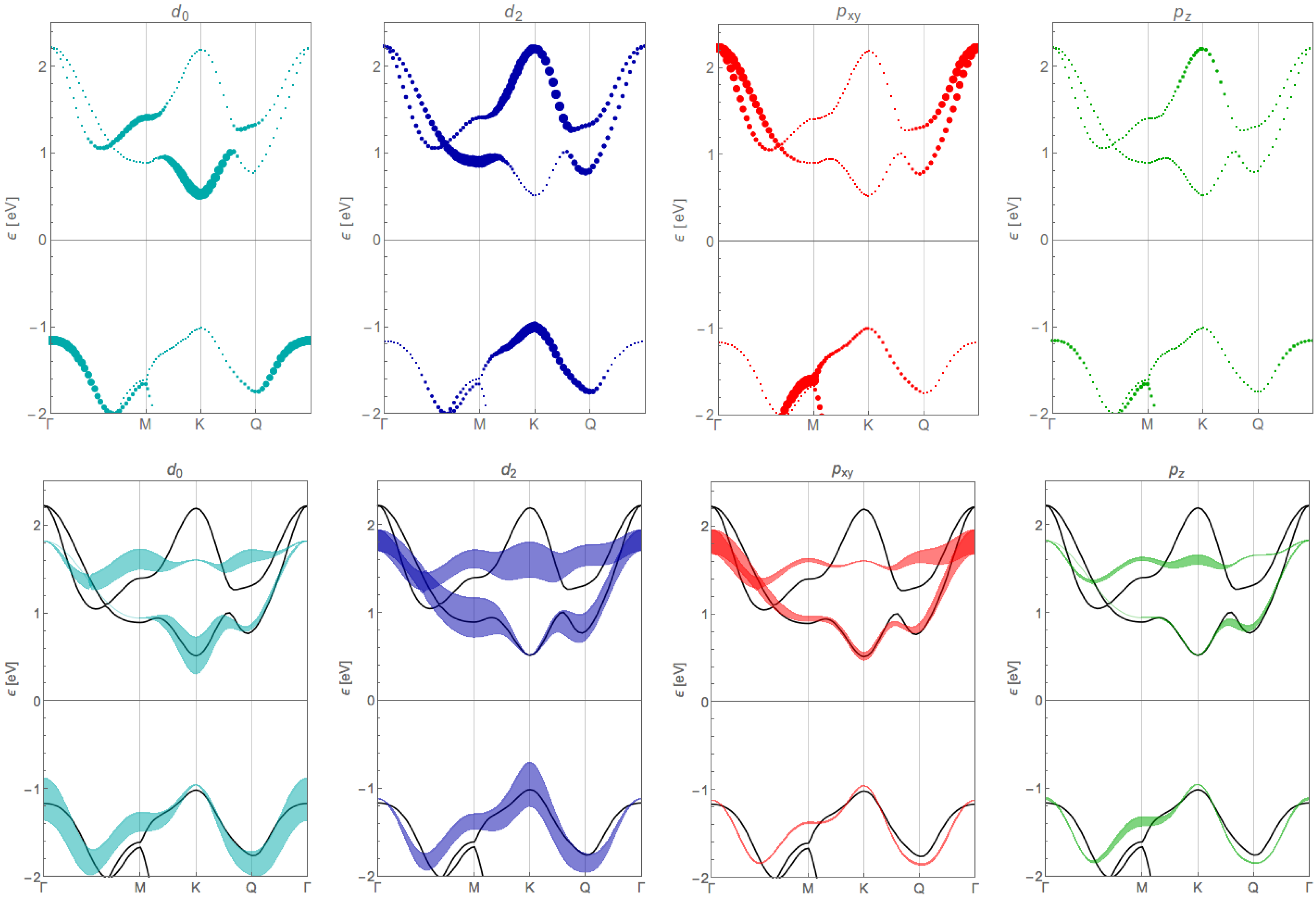
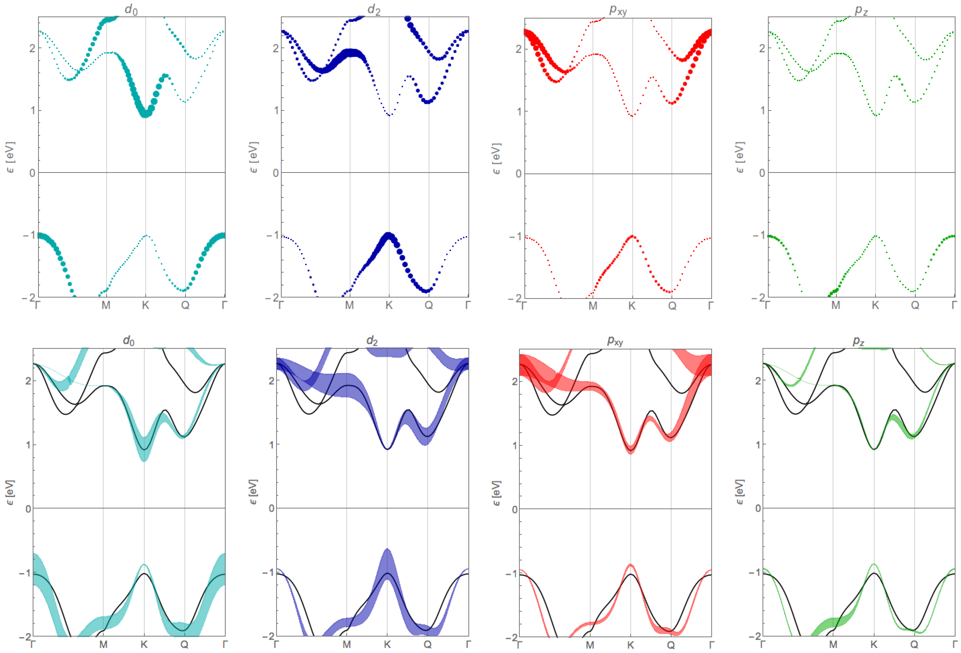
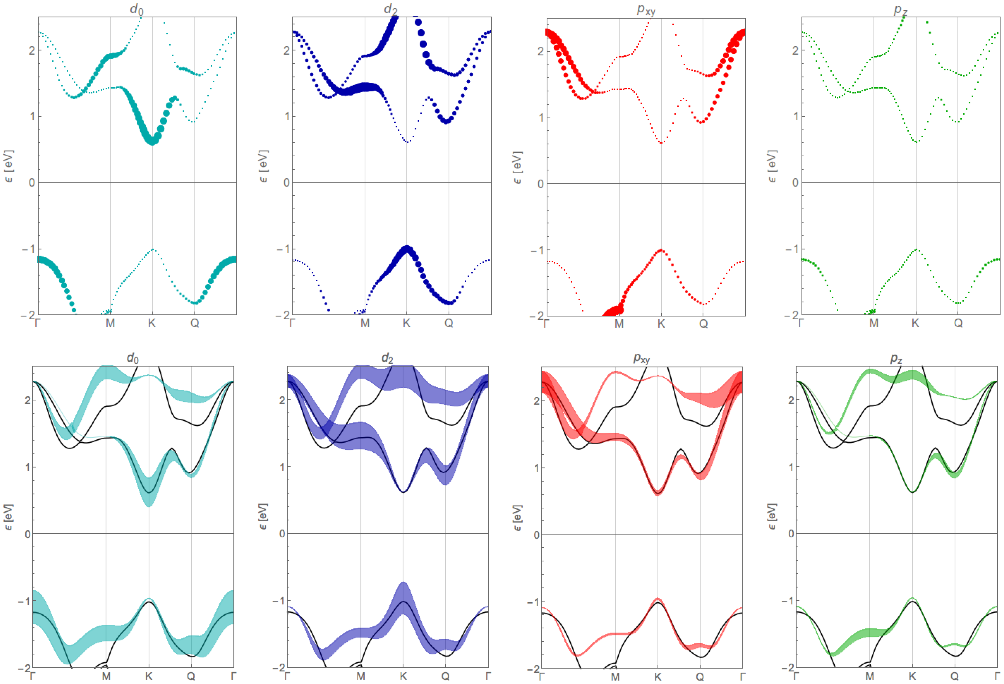
Appendix B. Orbital Contribution of the Tight-Binding Bands

In this appendix, we show the orbital contribution of the tight-binding bands, as compared to the DFT results, for MoSe 2 (Figure B1), WS 2 (Figure B2) and WSe 2 (Figure B3).
Figure B1. Same as Figure 4 but for MoSe 2 .
Applsci 06 00284 g006
Figure B2. Same as Figure 4 but for WS 2 .
Applsci 06 00284 g007
Figure B3. Same as Figure 4 but for WSe 2 .
Applsci 06 00284 g008

References

  1. Novoselov, K.S.; Jiang, D.; Schedin, F.; Booth, T.J.; Khotkevich, V.V.; Morozov, S.V.; Geim, A.K. Two-dimensional atomic crystals. Proc. Natl. Acad. Sci. USA 2005, 102, 10451–10453. [Google Scholar] [CrossRef] [PubMed]
  2. Wang, Q.H.; Kalantar-Zadeh, K.; Kis, A.; Coleman, J.N.; Strano, M.S. Electronics and optoelectronics of two-dimensional transition metal dichalcogenides. Nature Nanotech. 2012, 7, 699–712. [Google Scholar] [CrossRef] [PubMed]
  3. Jariwala, D.; Sangwan, V.K.; Lauhon, L.J.; Marks, T.J.; Hersam, M.C. Emerging Device Applications for Semiconducting Two-Dimensional Transition Metal Dichalcogenides. ACS Nano 2014, 8, 1102–1120. [Google Scholar] [CrossRef] [PubMed]
  4. Ganatra, R.; Zhang, Q. Few-Layer MoS2: A Promising Layered Semiconductor. ACS Nano 2014, 8, 4074–4099. [Google Scholar] [CrossRef] [PubMed]
  5. Feng, J.; Qian, X.; Huang, C.W.; Li, J. Strain-engineered artificial atom as a broad-spectrum solar energy funnel. Nat. Photonics 2012, 6, 866–872. [Google Scholar] [CrossRef]
  6. Pan, H.; Zhang, Y.W. Tuning the electronic and magnetic properties of MoS2 nanoribbons by strain engineering. J. Phys. Chem. C 2012, 116, 11752–11757. [Google Scholar] [CrossRef]
  7. Peelaers, H.; Van de Walle, C.G. Effects of strain on band structure and effective masses in MoS2. Phys. Rev. B 2012, 86. [Google Scholar] [CrossRef]
  8. Scalise, E.; Houssa, M.; Pourtois, G.; Afanas?ev, V.; Stesmans, A. First-principles study of strained 2D MoS2. Phys. E Low-Dimens. Syst. Nanostruct. 2014, 56, 416–421. [Google Scholar] [CrossRef]
  9. Molina-Sánchez, A.; Hummer, K.; Wirtz, L. Vibrational and optical properties of MoS2: From monolayer to bulk. Surf. Sci. Rep. 2015, 70, 554–586. [Google Scholar] [CrossRef]
  10. Brumme, T.; Calandra, M.; Mauri, F. First-principles theory of field-effect doping in transition-metal dichalcogenides: Structural properties, electronic structure, Hall coefficient, and electrical conductivity. Phys. Rev. B 2015, 91. [Google Scholar] [CrossRef]
  11. Zhu, Z.Y.; Cheng, Y.C.; Schwingenschlögl, U. Giant spin-orbit-induced spin splitting in two-dimensional transition-metal dichalcogenide semiconductors. Phys. Rev. B 2011, 84. [Google Scholar] [CrossRef]
  12. Xiao, D.; Liu, G.B.; Feng, W.; Xu, X.; Yao, W. Coupled Spin and Valley Physics in Monolayers of MoS2 and Other Group-VI Dichalcogenides. Phys. Rev. Lett. 2012, 108. [Google Scholar] [CrossRef] [PubMed]
  13. Xu, X.; Yao, W.; Xiao, D.; Heinz, T.F. Spin and pseudospins in layered transition metal dichalcogenides. Nat. Phys. 2014, 10, 343–350. [Google Scholar] [CrossRef]
  14. Babaee Touski, S.; Pourfath, M.; Roldán, R.; López-Sancho, M.P. Enhanced Spin-Flip Scattering by Surface Roughness in WS2 and MoS2 Nanoribbons. 2016; ArXiv e-prints. Available online: http://xxx.lanl.gov/abs/1606.03339 (accessed on 10 June 2016). [Google Scholar]
  15. Zeng, H.; Dai, J.; Yao, W.; Xiao, D.; Cui, X. Valley polarization in MoS2 monolayers by optical pumping. Nat. Nanotech. 2012, 7. [Google Scholar] [CrossRef] [PubMed]
  16. Mak, K.F.; He, K.; Sahn, J.; Heinz, T.F. Control of valley polarization in monolayer MoS2 by optical helicity. Nat. Nanotech. 2012, 7, 494–498. [Google Scholar] [CrossRef] [PubMed]
  17. Cao, T.; Wang, G.; Han, W.; Ye, H.; Zhu, C.; Shi, J.; Niu, Q.; Tan, P.; Wang, E.; Liu, B.; et al. Valley-selective circular dichroism of monolayer molybdenum disulphide. Nat. Commun. 2012, 3. [Google Scholar] [CrossRef] [PubMed]
  18. Zeng, H.; Liu, G.B.; Dai, J.; Yan, Y.; Zhu, B.; He, R.; Xie, L.; Xu, S.; Chen, X.; Yao, W.; et al. Optical signature of symmetry variations and spin-valley coupling in atomically thin tungsten dichalcogenides. Sci. Rep. 2013, 3. [Google Scholar] [CrossRef] [PubMed] [Green Version]
  19. Wu, S.; Ross, J.S.; Liu, G.B.; Aivazian, G.; Jones, A.; Fei, Z.; Zhu, W.; Xiao, D.; Yao, W.; Cobden, D.; et al. Electrical tuning of valley magnetic moment through symmetry control in bilayer MoS2. Nat. Phys. 2013, 9, 149–153. [Google Scholar] [CrossRef]
  20. Wang, Q.; Ge, S.; Li, X.; Qiu, J.; Ji, Y.; Feng, J.; Sun, D. Valley Carrier Dynamics in Monolayer Molybdenum Disulfide from Helicity-Resolved Ultrafast Pump–Probe Spectroscopy. ACS Nano 2013, 7, 11087–11093. [Google Scholar] [CrossRef] [PubMed]
  21. Mak, K.F.; He, K.; Lee, C.; Lee, G.H.; Hone, J.; Heinz, T.F.; Shan, J. Tightly bound trions in monolayer MoS2. Nat. Mat. 2013, 12. [Google Scholar] [CrossRef] [PubMed]
  22. Sallen, G.; Bouet, L.; Marie, X.; Wang, G.; Zhu, C.R.; Han, W.P.; Lu, Y.; Tan, P.H.; Amand, T.; Liu, B.L.; et al. Robust optical emission polarization in MoS2 monolayers through selective valley excitation. Phys. Rev. B 2012, 86. [Google Scholar] [CrossRef]
  23. Kormányos, A.; Zólyomi, V.; Drummond, N.D.; Burkard, G. Spin-Orbit Coupling, Quantum Dots, and Qubits in Monolayer Transition Metal Dichalcogenides. Phys. Rev. X 2014, 4. [Google Scholar] [CrossRef] [Green Version]
  24. Kormányos, A.; Burkard, G.; Gmitra, M.; Fabian, J.; Zólyomi, V.; Drummond, N.D.; Fal’ko, V. k * p theory for two-dimensional transition metal dichalcogenide semiconductors. 2D Mater. 2015, 2. [Google Scholar] [CrossRef]
  25. Roldán, R.; Castellanos-Gomez, A.; Cappelluti, E.; Guinea, F. Strain engineering in semiconducting two-dimensional crystals. J. Phys. Condens. Matter 2015, 27. [Google Scholar] [CrossRef] [PubMed]
  26. San-Jose, P.; Parente, V.; Guinea, F.; Roldán, R.; Prada, E. Inverse Funnel Effect of Excitons in Strained Black Phosphorus. Phys. Rev. X 2016, 6. [Google Scholar] [CrossRef]
  27. Wu, W.; Wang, L.; Li, Y.; Zhang, F.; Lin, L.; Niu, S.; Chenet, D.; Zhang, X.; Hao, Y.; Heinz, T.F.; et al. Piezoelectricity of single-atomic-layer MoS2 for energy conversion and piezotronics. Nature 2014, 514, 470–474. [Google Scholar] [CrossRef] [PubMed]
  28. Roldán, R.; Silva-Guillén, J.A.; López-Sancho, M.P.; Guinea, F.; Cappelluti, E.; Ordejón, P. Electronic properties of single-layer and multilayer transition metal dichalcogenides MX2 (M = Mo, W and X = S, Se). Ann. Phys. 2014, 526, 347–357. [Google Scholar] [CrossRef]
  29. Yuan, S.; Roldán, R.; Katsnelson, M.I.; Guinea, F. Effect of point defects on the optical and transport properties of MoS2 and WS2. Phys. Rev. B 2014, 90. [Google Scholar] [CrossRef]
  30. Rostami, H.; Roldán, R.; Cappelluti, E.; Asgari, R.; Guinea, F. Theory of strain in single-layer transition metal dichalcogenides. Phys. Rev. B 2015, 92. [Google Scholar] [CrossRef]
  31. Pearce, A.J.; Burkard, G. A Tight Binding Approach to Strain and Curvature in Monolayer Transition-Metal Dichalcogenides. 2015; ArXiv e-prints. Available online: http://xxx.lanl.gov/abs/1511.06254 (accessed on 22 November 2015). [Google Scholar]
  32. Rostami, H.; Asgari, R.; Guinea, F. Edge modes in zigzag and armchair ribbons of monolayer MoS2. 2015; ArXiv e-prints. Available online: http://xxx.lanl.gov/abs/1511.07003 (accessed on 22 November 2015). [Google Scholar]
  33. Farmanbar, M.; Amlaki, T.; Brocks, G. Green’s function approach to edge states in transition metal dichalcogenides. Phys. Rev. B 2016, 93. [Google Scholar] [CrossRef]
  34. Castellanos-Gomez, A.; Roldán, R.; Cappelluti, E.; Buscema, M.; Guinea, F.; van der Zant, H.S.J.; Steele, G.A. Local Strain Engineering in Atomically Thin MoS2. Nano Letters 2013, 13, 5361–5366. [Google Scholar] [CrossRef] [PubMed]
  35. Cappelluti, E.; Roldán, R.; Silva-Guillén, J.A.; Ordejón, P.; Guinea, F. Tight-binding model and direct-gap/indirect-gap transition in single-layer and multilayer MoS2. Phys. Rev. B 2013, 88. [Google Scholar] [CrossRef]
  36. Liu, G.B.; Shan, W.Y.; Yao, Y.; Yao, W.; Xiao, D. Three-band tight-binding model for monolayers of group-VIB transition metal dichalcogenides. Phys. Rev. B 2013, 88. [Google Scholar] [CrossRef]
  37. Kośmider, K.; González, J.W.; Fernández-Rossier, J. Large spin splitting in the conduction band of transition metal dichalcogenide monolayers. Phys. Rev. B 2013, 88. [Google Scholar] [CrossRef] [Green Version]
  38. Kumar, A.; Ahluwalia, P. Electronic structure of transition metal dichalcogenides monolayers 1H-MX2 (M= Mo, W; X= S, Se, Te) from ab-initio theory: new direct band gap semiconductors. Eur. Phys. J. B 2012, 85, 1–7. [Google Scholar] [CrossRef]
  39. Soler, J.; Artacho, E.; Gale, J.; García, A.; Junquera, J.; Ordejón, P.; Sánchez-Portal, D. The SIESTA method for ab initio order-N materials simulation. J. Phys. Condens. Matter 2002, 14, 2745–2779. [Google Scholar] [CrossRef]
  40. Artacho, E.; Anglada, E.; Dieguez, O.; Gale, J.; García, A.; Junquera, J.; Martin, R.; Ordejón, P.; Pruneda, J.M.; Sánchez-Portal, D.; Soler, J. The SIESTA method; developments and applicability. J. Phys. Condens. Matter 2008, 20. [Google Scholar] [CrossRef] [PubMed]
  41. Ceperley, D.; Alder, B.J. Ground State of the Electron Gas by a Stochastic Method. Phys. Rev. Lett. 1980, 45. [Google Scholar] [CrossRef]
  42. Perdew, P.; Zunger, A. Self-interaction correction to density-functional approximations for many-electron systems. Phys. Rev. B 1981, 23. [Google Scholar] [CrossRef]
  43. Artacho, E.; Sánchez-Portal, D.; Ordejón, P.; García, A.; Soler, J. Linear-Scaling ab-initio Calculations for Large and Complex Systems. Phys. Status Solidi B Basic Res. 1999, 215, 809–817. [Google Scholar] [CrossRef]
  44. Fernández-Seivane, L.; Oliveira, M.; Sanvito, S.; Ferrer, J. On-site approximation for spin-orbit coupling in linear combination of atomic orbitals density functional methods. J. Phys. Condens. Matter 2006, 18. [Google Scholar] [CrossRef]
  45. Bromley, R.A.; Murray, R.B.; Yoffe, A.D. The band structures of some transition metal dichalcogenides. III. Group VIA: trigonal prism materials. J. Phys. C Solid State Phys. 1972, 5. [Google Scholar] [CrossRef]
  46. Schutte, W.; Boer, J.D.; Jellinek, F. Crystal structures of tungsten disulfide and diselenide. J. Solid State Chem. 1987, 70, 207–209. [Google Scholar] [CrossRef]
  47. Kumar, A.; Ahluwalia, P.K. Electronic structure of transition metal dichalcogenides monolayers 1H-MX2 (M = Mo, W; X = S, Se, Te) from ab-initio theory: new direct band gap semiconductors. Eur. Phys. J. B 2012, 85. [Google Scholar] [CrossRef]
  48. Roldán, R.; López-Sancho, M.P.; Guinea, F.; Cappelluti, E.; Silva-Guillén, J.A.; Ordejón, P. Momentum dependence of spin–orbit interaction effects in single-layer and multi-layer transition metal dichalcogenides. 2D Mater. 2014, 1. [Google Scholar] [CrossRef]
  49. Slater, J.C.; Koster, G.F. Simplified LCAO Method for the Periodic Potential Problem. Phys. Rev. 1954, 94, 1498–1524. [Google Scholar] [CrossRef]
  50. Ridolfi, E.; Le, D.; Rahman, T.S.; Mucciolo, E.R.; Lewenkopf, C.H. A tight-binding model for MoS2 monolayers. J. Phys. Condens. Matter 2015, 27. [Google Scholar] [CrossRef] [PubMed]
  51. Fang, S.; Kuate Defo, R.; Shirodkar, S.N.; Lieu, S.; Tritsaris, G.A.; Kaxiras, E. Ab initio tight-binding Hamiltonian for transition metal dichalcogenides. Phys. Rev. B 2015, 92. [Google Scholar] [CrossRef]
  52. Lado, J.L.; Fernandez-Rossier, J. Landau Levels in two dimensional materials from first principles. 2016. ArXiv e-prints. [Google Scholar] [CrossRef]
  53. Mak, K.F.; Lee, C.; Hone, J.; Shan, J.; Heinz, T.F. Atomically Thin MoS2: A New Direct-Gap Semiconductor. Phys. Rev. Lett. 2010, 105. [Google Scholar] [CrossRef] [PubMed]
Figure 1. (a) Sketch of the atomic structure of MX 2 . The bulk compound has a 2H–MX 2 structure with two MX 2 layers per unit cell, each of them being built up from a trigonal prism coordination unit. The value of the lattice constants for each family is given in Table 1; (b) top view of monolayer M X 2 lattice. Green (blue) circles indicate M (X) atoms. The nearest neighbors ( δ i ) and the next nearest neighbors ( a i ) vector are shown in the figure.
Applsci 06 00284 g001
Figure 2. Two-dimensional Brillouin zone (BZ) of M X 2 . The high symmetry points Γ = ( 0 , 0 ) , K = 4 π / 3 a ( 1 , 0 ) and M = 4 π / 3 a ( 0 , 3 / 2 ) are shown. The Q points (which are not high symmetry points) indicate the position of the edges of the conduction band in multi-layer samples.
Applsci 06 00284 g002
Figure 3. Electronic band structure of single-layer M X 2 from Density Functional Theory (DFT) calculations (black lines) and from tight-binding (TB) (red lines).
Applsci 06 00284 g003
Figure 4. Band structure and orbital character of single-layer MoS 2 . The thickness of the bands represents the orbital weight, where the d character ( d 2 = d x 2 - y 2 , d x y and d 0 = d 3 z 2 - r 2 ) refers to the Mo atom 4 d orbitals, while the p character (where p x y = p x , p y ) refers to 3 p orbitals of sulfur. Top panels correspond to orbital weight from DFT calculations, whereas bottom panels correspond to orbital weight from TB results. The black lines in the bottom panels are the DFT bands. Notice that spin–orbit coupling is not included in these plots.
Applsci 06 00284 g004
Figure 5. Optical conductivity of the four compounds, calculated from the TB model. The insets show the respective low energy zooms of σ ( ω ) around the onset of optical transitions.
Applsci 06 00284 g005
Table 1. Lattice parameters for the TMDs (transition metal dichalcogenides) considered in the text. a represents the MM atomic distance, u the internal vertical separation between the M and the X planes, and c the distance between the metal M layers. In bulk systems, c = 2 c accounts for the z-axis lattice parameter. All values are in Å units.
au c
MoS 2 3 . 160 1 . 586 6 . 140
MoSe 2 3 . 288 1 . 664 6 . 451
WS 2 3 . 153 1 . 571 6 . 160
WSe 2 3 . 260 1 . 657 6 . 422
Table 2. Spin–orbit coupling λ α and tight-binding parameters for single-layer M X 2 , where the metal M is Mo or W and X is S or Se. All of the Slater–Koster parameters are in units of eV. Spin-Orbit (SO) coupling parameters are taken from Reference [37].
MoS 2 MoSe 2 WS 2 WSe 2
SOC λ M   0.086  0.089  0.271  0.251
λ X   0.052  0.256  0.057 0.439
Crystal Fields Δ 0 −1.094  −1.144−1.155−0.935
Δ 1 −0.050  −0.250−0.650−1.250
Δ 2 −1.511  −1.488−2.279−2.321
Δ p −3.559  −4.931−3.864−5.629
Δ z −6.886  −7.503−7.327−6.759
MX V p d σ 3.689  3.7287.9115.803
V p d π −1.241  −1.222−1.220−1.081
MM V d d σ −0.895  −0.823−1.328−1.129
V d d π 0.252  0.2150.1210.094
V d d δ 0.228  0.1920.4420.317
XX V p p σ 1.225  1.2561.1781.530
V p p π −0.467  −0.205−0.273−0.123
Table 3. Comparison of the orbital contribution at band edges at K and Γ points obtained from DFT (Density Functional Theory) and TB (tight-binding) models. K v (K c ) refers to the edge of the valence (conduction) band at K point, and Γ v refers to the edge of the valence band at the Γ point.
K v K c Γ v
DFTTBDFTTBDFTTB
MoS 2 d 0 0.00.00.820.770.660.96
d 2 0.761.00.00.00.00.0
p x y 0.200.00.120.230.00.0
p z 0.00.00.00.000.280.04
MoSe 2 d 0 0.00.00.830.830.710.96
d 2 0.781.00.00.00.00.0
p x y 0.180.00.100.170.00.0
p z 0.00.00.00.00.230.04
WS 2 d 0 0.00.00.800.760.640.98
d 2 0.740.940.00.00.00.0
p x y 0.210.060.070.240.00.0
p z 0.00.00.00.00.280.02
WSe 2 d 0 0.00.00.820.860.690.99
d 2 0.730.950.00.00.00.0
p x y 0.200.050.050.140.00.0
p z 0.00.00.00.00.230.01

