Article

Optical and Transport Properties of Ni-MoS2

Department of Electronic Engineering, National Changhua University of Education, No.2, Shi-Da Road, Changhua City, Changhua County 500, Taiwan
*
Author to whom correspondence should be addressed.
Submission received: 7 June 2016 / Accepted: 8 August 2016 / Published: 12 August 2016
(This article belongs to the Special Issue Two-Dimensional Transition Metal Dichalcogenides)

Abstract

:
In this paper, MoS2 and Ni-MoS2 crystal layers were fabricated by the chemical vapor transport method with iodine as the transport agent. Two direct band edge transitions of excitons at 1.9 and 2.1 eV were observed successfully for both MoS2 and Ni-MoS2 samples using temperature-dependent optical reflectance (R) measurement. Hall effect measurements were carried out to analyze the transport behavior of carriers in MoS2 and Ni-MoS2, which indicate that the Ni-MoS2 sample is n-type and has a higher resistance and lower mobility than the MoS2 sample has. A photoconductivity spectrum was performed which shows an additional Ni doping level existing at 1.2 eV and a higher photocurrent generating only for Ni-MoS2. The differences between MoS2 and Ni-MoS2 could be attributed to the effect of Ni atoms causing small lattice imperfections to form trap states around 1.2 eV. The temperature-dependent conductivity shows the presence of two shallow levels with activation energies (84 and 6.7 meV in MoS2; 57 and 6.5 meV in Ni-MoS2). Therefore, the Ni doping level leads to high resistance, low mobility and small activation energies. A series of experimental results could provide useful guidance for the fabrication of optoelectronic devices using MoS2 structures.

Graphical Abstract

1. Introduction

In recent years, transition metal dichalcogenides (TMDCs) have attracted great attention owing to their two-dimensional layer structure which is analogous to graphene [1,2]. As a member of the TMDC family, molybdenum disulfide (MoS2) with a direct bandgap is complementary to the graphene and suggests a great potential for logic devices, integrated circuits, and optoelectronics [3,4,5,6]. Therefore, MoS2 is rallied up as a finite-energy-bandgap alternative to graphene in advanced electronic and photonic device applications [7,8,9,10,11]. Several interesting properties of MoS2 have been also studied in terms of the optical properties and electrical structure. For example, Ayari et al. reported there is a transition for MoS2 from an indirect bandgap in the bulk to a direct gap in the few-layer structures [12], which would be desirable and beneficial for TMDC transistor development. Kadantsev et al. investigated the electronic structure of a single MoS2 monolayer using first-principles calculations [13], and their results point out that a single MoS2 monolayer is a direct K to K bandgap semiconductor. Howell et al. studied discontinuous characteristics in energy bands that exist at the interface of monolayer and multilayer thin films [14]. Amani et al. carried out a detailed study to understand the behavior of the electrical performance of monolayer MoS2 field-effect transistors using the chemical vapor deposition method [15]. Furthermore, Kenneth et al. demonstrated near-field electrical detection of silver nanowire plasmons with the atomically thin semiconductor molybdenum disulfide [16]. In spite of many relevant MoS2 characteristics being determined, so far little is known about the properties of the doping categories and their effect on optical and electrical characteristics in terms of whether MoS2 is a monolayer or bulk. A stable p-type MoS2 is important for TMDC device applications and has been performed by Nb doping against the native n-type propensity in unintentionally doped MoS2 [17]. In that study a stable p-type conduction with a degenerate hole density of ~3 × 1019 cm−3 in MoS2 has been demonstrated. Furthermore, Guha et al. pointed out that natural MoS2 was p-type in the early period [18]. Nevertheless, most studies revealed that MoS2 ought to be n-type [19,20]. Among these studies on dopants, little information has been published concerning the material and physical properties for Ni-MoS2 thin film. Herein, we have also undertaken a series of experiments to analyze the optical and electrical properties of pure MoS2 and Ni-MoS2.
In this paper, both MoS2 samples with and without the Ni dopant were prepared by the chemical vapor transport (CVT) method. In terms of optical and electrical properties, reflectance (R), transmittance, photoconductivity (PC), and Hall effect measurements were carried out for both samples. A series of experiments results confirmed the Ni dopant effect on fundamental material properties which could provide guidance for further electronic and optoelectronic devices of MoS2.

2. Experimental Details

The MoS2 single crystals were grown by the CVT method for this study, using I2 as a transporting agent. The iodine transport agent and the elements including Mo (99.99%), S (99.99%) and Ni (99.99%) were used for the crystal growth. The molar ratio of Mo/S is 1:2. The intentional doping concentration of Ni is 0.5%. Afterward, whole reactants were placed in quartz tubes which were evacuated to 2 × 10⁻⁵ torr and sealed. For growing the crystals, the quartz tube was placed in a three-zone furnace and grown at 1000 °C for 720 h. In order to obtain an optimal diffusion gradient for crystal growth, the temperature gradient was adjusted at 1050 to 935 °C. We carried out electron spectroscopy for chemical analysis (ESCA) for Ni-MoS2 to confirm existence of elements like nickel or iodine. Figure 1a,b shows the ESCA results which indicate our Ni-MoS2 actually has Ni atoms with low percentage of 0.2%. No iodine was detected for both samples using ESCA analysis which provides evidence that probably only a few iodine atoms in both samples. The sample surface was observed using an homemade optical microscope (OM) system. A 150 W Xenon lamp equipped with a PTI 0.25 m monochromator was used to provide monochromatic light which was chopped by a mechanical chopper at frequency of 200 Hz for R measurement. The monochromatic light reflected from the sample surface. Consequently the light was collected by lens, detected by a photomultiplier tube (PMT) and recorded by a lock-in amplifier. Meanwhile, a closed-cycle cryostat was utilized to control the temperature changing from 20 to 300 K for R experiment. The same light source and similar setup were also employed in PC and transmittance experiments. As for PC measurements, the sample was connected in series to a resistor (10 kΩ) and a constant voltage (1 V) to complete a circuit loop. The frequency of probe light was chopped and fixed 7 Hz. We utilized van der Pauw method to carry out Hall effect measurement at room temperature. The electrical properties of MoS2 and Ni-MoS2 were investigated including carrier concentration, resistance and mobility. Since the shape of sample is irregular, the four contacts were made to sides in square shape located at the edges of the sample with the same distance between each contact [21]. The temperature-dependent I-V measurements from 20 to 300 K were also carried out in a closed-cycle He-crysostat for temperature conductivity analysis. The samples were illuminated with monochromatic light of 1.2 eV filtered from a xenon lamp.

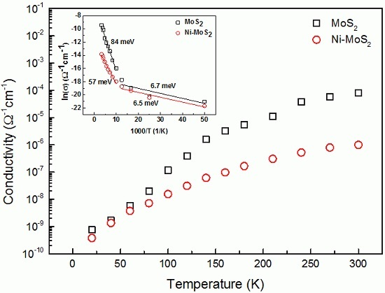
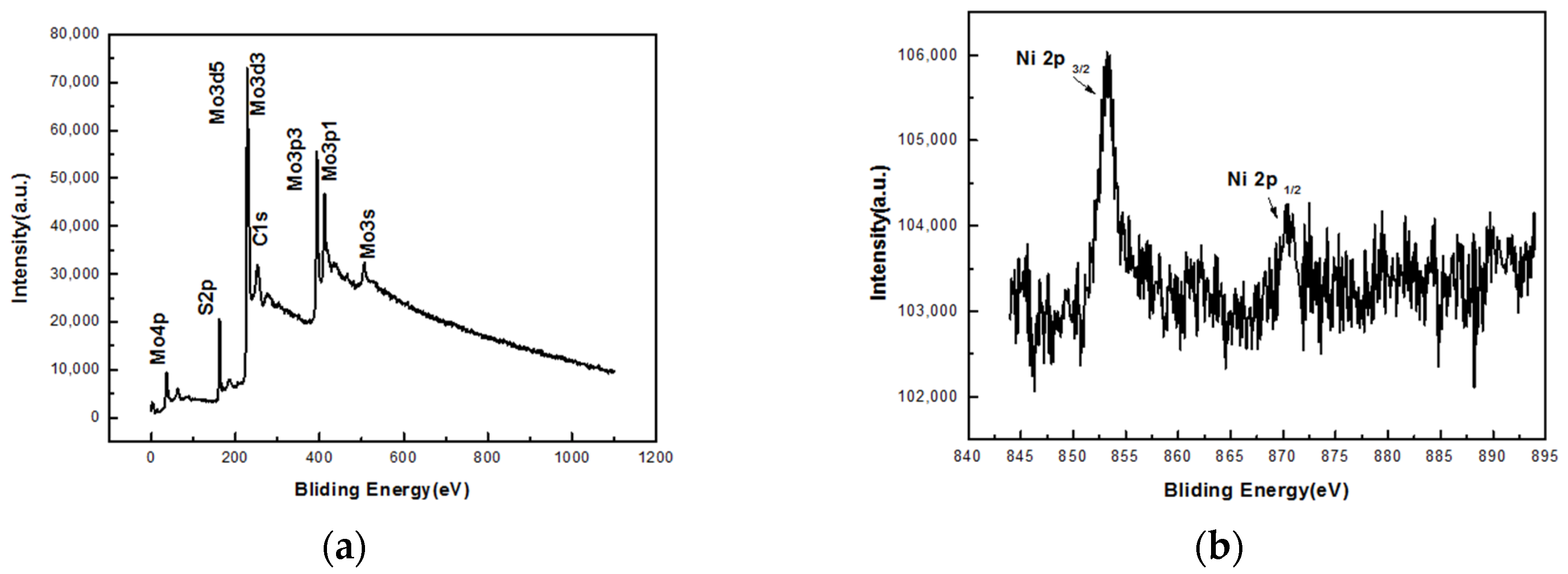
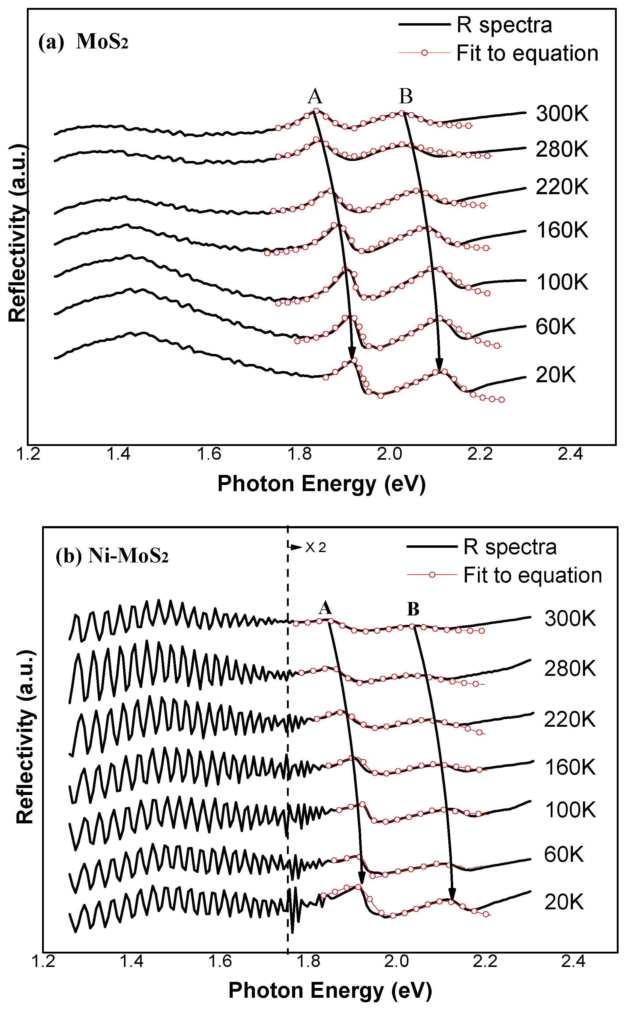
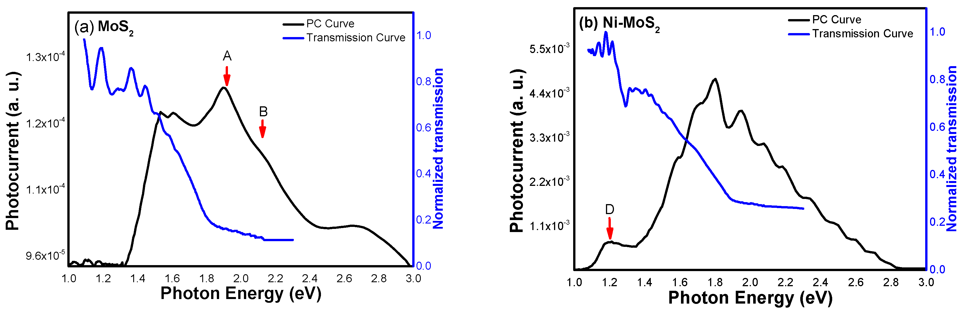
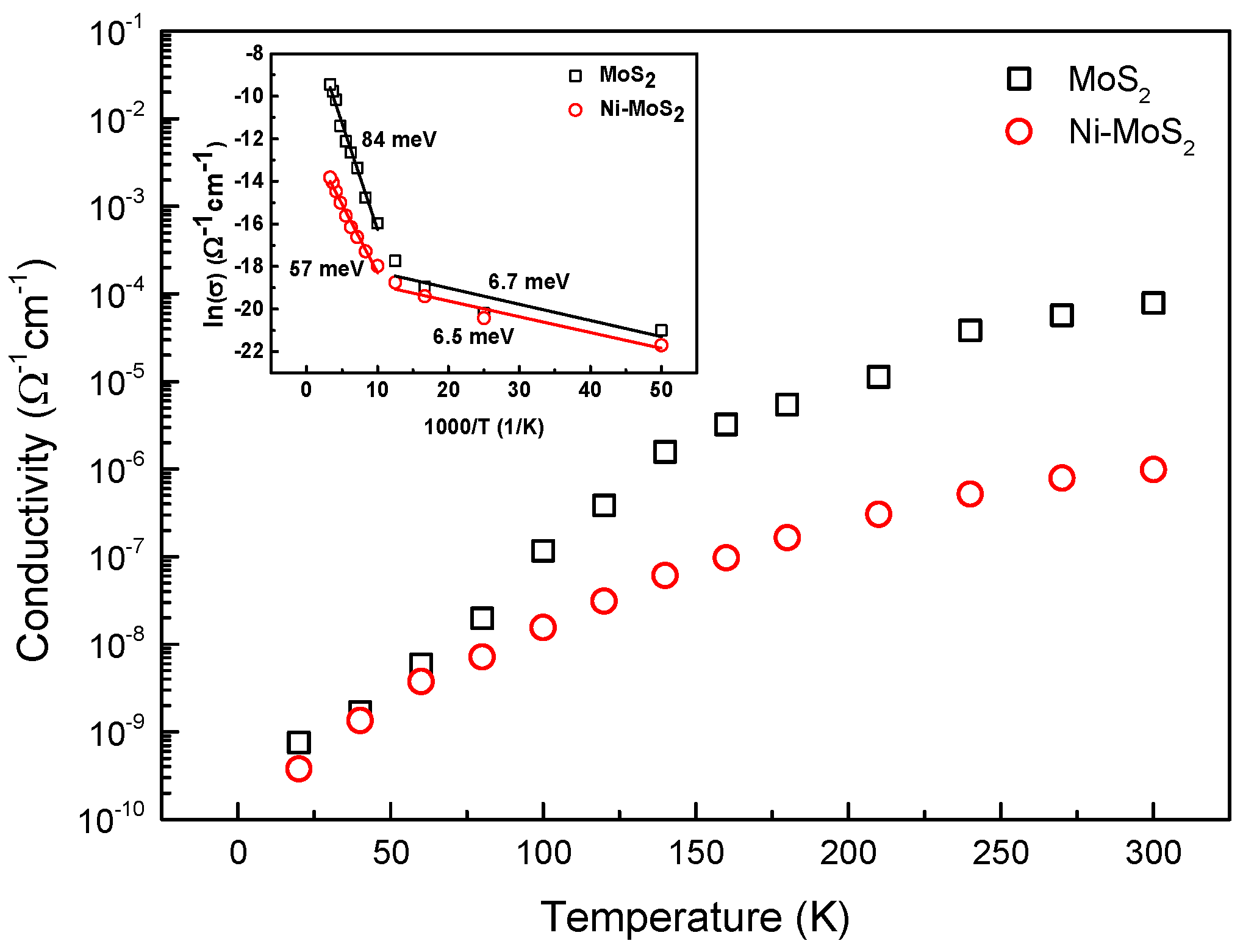
3. Results and Discussion

The samples were formed with many stacked layers after growth. The thickness of the layered MoS2 crystal is about 20 μm. The three-dimensional crystal is formed by stacking the two-dimensional MoS2 sheets. Since there is the interaction of a weak van der Waals force providing a natural cleavage plane of the crystal between two adjacent MoS2 sheets [22], it would be easy to separate the samples into thin specimens with a smooth surface. The OM images of MoS2 and Ni-MoS2 are presented in Figure 2. According to previous literature, the optical micrograph image of the surface of 2H MoS2 may show a hexagonal shape, while that of 3R MoS2 may show a triangular shape [23,24]. In our case, both images show the feature with hexagonal corners (γ = 120 degrees) on the surface, indicating that the MoS2 samples are 2H single crystals. The smooth surfaces of MoS2 are beneficial for performing the R measurements [25].
In order to understand exciton behavior in MoS2 and Ni-MoS2, temperature-dependent R spectra were carried out at a temperature range of 20 to 300 K for both MoS2 and Ni-MoS2 samples. The results of the R spectra of the MoS2 and Ni-MoS2 indicate two main resonance features existing in each spectrum for both samples, as Figure 3 shows. We analyzed these spectra using the below Equation (1) proposed by Korona et al. [26]
R ( v ) = R o + R x R e [ h v x h v + i Γ x Γ x 2 + ( h v h v x ) 2 ] i Θ
where R o is the background, R x is the intensity, h v x is the photon energy, Γ x is the broadening parameter and Θ is the phase. Afterward, two obvious peaks at 1.83 and 2.02 eV were obtained and denoted as A and B at 300 K, respectively. The energy difference between A and B excitonic transitions is 0.15 eV [23]. Furthermore, the values of features A and B are a little lower than those observed in the absorption peaks and photoluminescence peaks of atomically thin MoS2 samples [9], which could explain these two features arising from direct bandgap transitions between the maxima of split valance bands (v1 and v2) and the minimum of the conduction band (c1). The valance band was split due to the combined effects including the interlayer and spin-orbit coupling [27]. Both features are gradually shifted to the slight highly 1.91 and 2.11 eV, respectively, when the temperature is ramped down to 20 K due to less thermal activation. In addition, both direct bandgap transitions A and B in the R spectra of the Ni-MoS2 are very close to that of the MoS2 under different temperatures. Therefore, this result could indirectly reflect that the MoS2 crystal structure did not suffer from much distortion even though Ni atoms were doped. On the other hand, the interference feature could be found only in the R spectrum of Ni-MoS2. This could be attributed to the poor surface roughness of the MoS2 we picked up for measurement.
Here we adopted the Varshni equation, Eg(T) = Eg(0) − (αT2/(T + β)), to describe the bandgap reduction with the temperature [28]. The constant α is related to the electron-phonon and β is related to the Debye temperature. The spectral shift of the A and B features with the energy is depicted in Figure 4. Furthermore, another analysis method was also considered which was proposed by O’Donnell and Chen [29]. The empirical expression is shown as below in Equation (2).
E i e x ( T ) = E i e x ( 0 ) S Ω [ coth Ω 2 K T 1 ]
where Eiex(0) is the band bap at 0 K, S is a dimensionless coupling constant, and ħΩ is an average phonon energy. By fitting the Varshni equation (red line) and O’Donnell’s empirical expression (blue line), the temperature dependence of the A and B transitions could be obtained. The fitted parameters are listed in Table 1. The trend and fitted parameters shown here have a reasonable consistency with similar results of reflection of the MoS2 as proposed by Ho et al. [30]. Therefore, the temperature shift of excitonic-transition energies could be attributed to both the lattice variations and interactions with relevant acoustic and optical phonons.
Room-temperature Hall effect measurements were performed for MoS2 and Ni-MoS2. The relevant results are shown in Table 2. The Hall effect measurement results indicate that the carrier types of the MoS2 and Ni-MoS2 samples are n-type. The mobilities of the MoS2 and Ni-MoS2 samples are 78.51 and 1.87 cm2V−1s−1, respectively. The resistance was increased about 40 times when Ni was doped into MoS2. Although the Hall effect measurements also indicate that the Ni-MoS2 possesses a similar carrier density of ~ 1.1 × 1013 cm−2 as MoS2 does, Ni-MoS2 still has a lower mobility and higher resistance than the undoped MoS2 has. These results confirm that Ni atoms could not contribute additional electrons or electron holes in MoS2. On the contrary, these Ni atoms seem to form defects/traps to obstruct electron flows. Meanwhile, Ni dopants produced a band tailing effect due to slight crystal distortion, resulting in the A and B peaks for Ni-MoS2 being slightly lower than those for MoS2.
We implemented PC measurements using a DC bias of 1 V, which records the alternating current induced by the ON/OFF illumination controlled by a mechanical chopper at a frequency of 7 Hz at different photo energies. Meanwhile, transmittance was also carried out at 20 K for comparison. The low temperature PC and transmittance spectrum measured at 20 K are shown in Figure 5. PC results indicate that the main peaks A and B were also observed for both MoS2 and Ni-MoS2 samples, which is consistent with previous R measurements. In additions, there is an extra signal that occurs at 1.2 eV, indicated by D. However, no obvious peak could be found at 1.2 eV for the MoS2. For the Ni-MoS2 sample, this peak D could be attributed to Ni dopants that induce an additional Ni doping level, providing a different transition path of carriers. In addition, the whole PC spectrum of Ni-MoS2 is wider than that of undoped MoS2, which leads to ambiguous A and B positions in the PC spectrum of Ni-MoS2. Since Ni dopants not only introduce a doping level but also some impurities or defects that cause additional deep levels in the forbidden band, these multi-levels probably result in an obvious and wide width in the PC spectrum of Ni-MoS2. As for the transmittance results, we carried out transmission experiments for samples after exfoliating them several times. The normalized transmission results for MoS2 and Ni-MoS2 have been also included in Figure 5. The ratio of normalized transmission gradually decreased from 1.3 to 1.9 eV due to absorption. However, a low transmission still could be found above 1.9 eV, which could be attributed to some tiny cracks. These cracks were probably produced during the exfoliating process and led to samples that could not absorb the whole photoenergy. In contrast, there is no doping state in the PC spectrum except for both clear A and B excitons, which is consistent with the reflectance results. Since these electrons in the doping state transit to the conduction band, it is worth noting that the photocurrent has been enhanced up to several tens of times and the response wavelength has also been extended when Ni is doped in MoS2. This result indicates that the doping is a good way to improve their applications in light responsibility for solar cells and photo detectors.
In order to understand the temperature dependence and the activation energy of the Ni-induced defect in MoS2, we carried out temperature-dependent I-V measurements and analyzed the temperature-dependent conductivity of MoS2 and Ni-MoS2 for the calculation of activation energy. The samples were illuminated with a monochromatic light of 1.2 eV filtered from a xenon lamp. A typical semiconducting transport behavior is observed for both samples from the conductivity (σ)-T plot shown in Figure 6. The σ decreases gradually while lowering the temperature from 300 to 20 K. The inset in Figure 6 shows the Arrhenius plot of both samples. It is possible to obtain information about the activation energy by analyzing the experimental data on the basis of the following relation (3):
σ = σ0 × exp(−Ea/kT)
where σ0 is the preexponential factor, Ea is the activation energy and k is the Boltzmann constant. For MoS2, two different slopes can roughly be differentiated and the corresponding values of activation energy Ea are calculated as Ea1 = 84 meV and Ea2 = 6.7 meV, respectively. On the other hand, activation energy Ea of Ni-MoS2 is 57 meV for Ea1 and 6.5 meV for Ea2. These results indicate the presence of shallower donors in Ni-MoS2. In principle, smaller Ea values in Ni-MoS2 could be attributed to Ni-induced donor defects or related impurities.

4. Conclusions

In conclusion, both MoS2 and Ni-MoS2 samples were grown by the CVT method. Two direct transitions and one indirect transition for both samples were observed successfully via R spectra analysis. Although the Hall effect measurements indicate that MoS2 and Ni-MoS2 possesses a similar carrier concentration, the Ni-MoS2 still has a lower mobility and higher resistance than the undoped MoS2 has. The characteristics of the n-type carrier were confirmed for both samples simultaneously. PC measurements reveal Ni dopants introducing an additional deep Ni doping level existing at 1.2 eV for the Ni-MoS2 sample which also enhanced the photocurrent. In addition, two shallow activation energies (Ea1 = 84 meV and Ea2 = 6.7 meV) in MoS2 and (Ea1 = 57 meV and Ea2 = 6.5 meV) Ni-MoS2 have been defined in this study. Smaller Ea values in Ni-MoS2 could be attributed to Ni-induced donor defects or a related impurity. These results confirm Ni atoms which could not contribute additional electrons or electron holes in MoS2. Instead, Ni dopants in MoS2 would introduce an additional deep level at 1.2 eV causing high resistance and low mobility.

Acknowledgments

This study was supported by the Ministry of Science and Technology of Taiwan, Republic of China under Contracts MOST 104-2221-E-018-017 and MOST 104-2112-M-018-004.

Author Contributions

D.-Y.L. conceived and designed the experiments; C.-C.H. performed the experiments; T.-S.K. and D.-Y.L. analyzed the data; D.-Y.L. contributed reagents/materials/analysis tools; T.-S.K. and D.-Y.L. wrote the paper.

Conflicts of Interest

The authors declare no conflict of interest.

References

  1. Balandin, A.A.; Ghosh, S.; Bao, W.; Calizo, I.; Teweldebrhan, D.; Miao, F.; Lau, C.N. Deoxygenation of exfoliated graphite oxide under alkaline conditions: A green route to graphene preparation. Nano Lett. 2008, 8, 902–907. [Google Scholar] [CrossRef] [PubMed]
  2. Mayorov, A.S.; Gorbachev, R.V.; Morozov, S.V.; Britnell, L.; Jalil, R.; Ponomarenko, L.A.; Blake, P.; Novoselov, K.S.; Watanabe, K.; Taniguchi, T.; et al. Micrometer-scale ballistic transport in encapsulated graphene at room temperature. Nano Lett. 2011, 11, 2396–2399. [Google Scholar] [CrossRef] [PubMed]
  3. Gourmelon, E.; Lignier, O.; Hadouda, H.; Couturier, G.; Bernede, J.C.; Tedd, J.; Pouzed, J.; Salardenne, J. Solar Energy materials and solar cells. Sol. Energy Mater. Sol. Cells 1997, 46, 115–121. [Google Scholar] [CrossRef]
  4. Ho, W.K.; Yu, J.C.; Lin, J.; Yu, J.G.; Li, P.S. Preparation and photocatalytic behavior of MoS2 and WS2 nanocluster sensitized TiO2. Langmuir 2004, 20, 5865–5869. [Google Scholar] [CrossRef] [PubMed]
  5. Wu, C.C.; Jariwala, D.; Sangwan, V.K.; Marks, T.J.; Hersam, M.C.; Lauhon, L.J. Elucidating the photoresponse of ultrathin MoS2 field-effect transistors by scanning photocurrent microscopy. J. Phys. Chem. Lett. 2013, 4, 2508–2513. [Google Scholar] [CrossRef]
  6. Yamaguchi, H.; Blancon, J.C.; Kappera, R.; Lei, S.; Najmaei, S.; Mangum, B.D.; Gupta, G.; Ajayan, P.M.; Lou, J.; Chhowalla, M.; et al. Spatially Resolved photoexcited charge-carrier dynamics in phase-engineered monolayer MoS2. ACS Nano 2015, 9, 840–849. [Google Scholar] [CrossRef] [PubMed]
  7. Novoselov, K.S.; Geim, A.K.; Morozov, S.V.; Jiang, D.; Katsneison, M.I.; Grigorieva, I.V.; Dubonos, S.V.; Firsov, A.A. Two-dimensional gas of massless Dirac fermions in graphene. Nature 2005, 438, 197–200. [Google Scholar] [CrossRef] [PubMed] [Green Version]
  8. Zhang, Y.; Tan, Y.W.; Stormer, H.L.; Kim, P. Experimental observation of the quantum Hall effect and Berry’s phase in graphene. Nature 2005, 438, 201–204. [Google Scholar] [CrossRef] [PubMed]
  9. Qiu, H.; Pan, L.; Yao, Z.; Li, J.; Shi, Y.; Wang, X. Electrical characterization of back-gated bi-layer MoS2 field-effect transistors and the effect of ambient on their performances. Appl. Phys. Lett. 2012, 100, 123104–123106. [Google Scholar] [CrossRef]
  10. Radisavljevic, B.; Radenovic, A.; Brivio, J.; Giacometti, V.; Kis, A. Single-layer MoS2 transistors. Nat. Nano Technol. 2011, 6, 147–150. [Google Scholar] [CrossRef] [PubMed]
  11. Jariwala, D.; Sangwan, V.K.; Lauhon, L.J.; Marks, T.J.; Hersam, M.C. Emerging device applications for semiconducting two-dimensional transition metal dichalcogenides. ACS Nano 2014, 8, 1102–1120. [Google Scholar] [CrossRef] [PubMed]
  12. Ayari, A.; Cobas, E.; Ogundadegbe, O.; Fuhrer, M.S. Two-dimensional nanosheets produced by liquid exfoliation of layered materials. J. Appl. Phys. 2007, 101, 014507–014511. [Google Scholar] [CrossRef]
  13. Kadantsev, E.S.; Hawrylak, P. Electronic structure of a single MoS2 monolayer. Solid State Commun. 2012, 153, 909–913. [Google Scholar] [CrossRef]
  14. Howell, S.L.; Jariwala, D.; Wu, C.C.; Chen, K.S.; Sangwan, V.K.; Kang, J.; Marks, T.J.; Hersam, M.C.; Lauhon, L.J. Investigation of band-offsets at monolayer–multilayer MoS2 junctions by scanning photocurrent microscopy. Nano Lett. 2015, 15, 2278–2284. [Google Scholar] [CrossRef] [PubMed]
  15. Matthew, M.A.; Chin, L.; Birdwell, A.G.; O’Regan, T.P.; Najmaei, S.; Liu, Z.; Ajayan, P.M.; Lou, J.; Dubey, M. Electrical characterization of back-gated bi-layer MoS2 field-effect transistors and the effect of ambient on their performances. Appl. Phys. Lett. 2013, 102, 193107–193109. [Google Scholar]
  16. Goodfellow, K.M.; Chakraborty, C.; Beams, R.; Novotny, L.; Vamivakas, A.N. Direct on-chip optical plasmon detection with an atomically thin semiconductor. Nano Lett. 2015, 15, 5477–5481. [Google Scholar] [CrossRef] [PubMed]
  17. Suh, J.; Park, T.E.; Lin, D.Y.; Fu, D.; Park, J.; Jung, H.J.; Chen, Y.; Ko, C.; Jang, C.; Sun, Y.; et al. Doping against the native propensity of MoS2: Degenerate hole doping by cation substitution. Nano Lett. 2014, 14, 6976–6982. [Google Scholar] [CrossRef] [PubMed]
  18. Thakurta, S.R.G.; Dutta, A.K. Electrical conductivity, thermoelectric power and Hall effect in p-type molybdenite (MoS2) crystal. J. Phys. Chem. Solids 1983, 44, 407–416. [Google Scholar] [CrossRef]
  19. Fivaz, R.; Mooser, E. Mobility of charge carriers in semiconducting layer structures. Phys. Rev. 1967, 163, 743–755. [Google Scholar] [CrossRef]
  20. Kim, S.; Konar, A.; Hwang, W.S.; Lee, J.H.; Lee, J.; Yang, J.; Jung, C.; Kim, H.; Yoo, J.B.; Choi, J.Y.; et al. High-mobility and low-power thin-film transistors based on multilayer MoS2 crystals. Nat. Commun. 2012, 3, 1011–1017. [Google Scholar] [CrossRef] [PubMed]
  21. Van Der Pauw, L.J. A method of measuring specific resistivity and Hall effect of discs of arbitrary shape. Philips Tech. Rev. 1958, 20, 220–224. [Google Scholar]
  22. Park, K.T.; Babb, M.R.; Freund, M.S.; Weiss, J.; Klier, K. Surface structure of single-crystal MoS2 (0002) and Cs/MoS2 (0002) by X-ray photoelectron diffraction. J. Phys. Chem. 1996, 100, 10739–10745. [Google Scholar] [CrossRef]
  23. Suzuki, R.; Sakano, M.; Zhang, Y.J.; Akashi, R.; Morikawa, D.; Harasawa, A.; Yaji, K.; Miyamoto, K.; Okuda, T.; Ishizaka, K.; et al. Valley-dependent spin polarization in bulk MoS2 with broken inversion symmetry. Nat. Nano Technol. 2014, 9, 611–617. [Google Scholar] [CrossRef] [PubMed]
  24. Andersen, A.; Kathmann, S.M.; Lilga, M.A.; Albrecht, K.O.; Hallen, R.T.; Mei, D. First-principles characterization of potassium intercalation in hexagonal 2H-MoS2. J. Phys. Chem. C 2012, 116, 1826–1832. [Google Scholar] [CrossRef]
  25. Wang, Q.H.; Kalantar-Zadeh, K.; Kis, A.; Coleman, J.N.; Strano, M.S. Electronics and optoelectronics of two-dimensional transition metal dichalcogenides. Nat. Nano Technol. 2012, 7, 699–712. [Google Scholar] [CrossRef] [PubMed]
  26. Korona, K.P.; Wysmolek, A.; Pakula, K.; Stepniewski, R.; Baranowski, J.M.; Grzegory, I.; Lucznik, B.; Wroblewski, M.; Porowski, S. Exciton region reflectance of homoepitaxial GaN layers. Appl. Phys. Lett. 1996, 69, 788–790. [Google Scholar] [CrossRef]
  27. Xiao, D.; Liu, G.B.; Feng, W.; Xu, X.; Yao, W. Coupled spin and valley physics in monolayers of MoS2 and other group-VI dichalcogenides. Phys. Rev. Lett. 2012, 108, 196802–196804. [Google Scholar] [CrossRef] [PubMed]
  28. Varshni, Y.P. Temperature dependence of the energy gap in semiconductors. Physica 1967, 34, 149–154. [Google Scholar] [CrossRef]
  29. O’Donnell, K.P.; Chen, X. Temperature dependence of semiconductor band gaps. Appl. Phys. Lett. 1991, 58, 2924–2926. [Google Scholar] [CrossRef]
  30. Ho, C.H.; Wu, C.S.; Huang, Y.S.; Liao, P.C.; Tiong, K.K. Temperature dependence of energies and broadening parameters of the band-edge excitons of Mo1-xWxS2 single crystals. J. Phys. Condens. Matter. 1998, 10, 9317–9328. [Google Scholar] [CrossRef]
Figure 1. Electron spectroscopy for chemical analysis (ESCA) results of (a) full spectrum and (b) high resolution in Ni region for Ni-MoS2.
Applsci 06 00227 g001
Figure 2. (Optical microscope) OM images of (a) MoS2 and (b) Ni-MoS2 under 30× magnification.
Applsci 06 00227 g002
Figure 3. Temperature-dependent reflection spectra of (a) MoS2 and (b) Ni-MoS2 samples.
Applsci 06 00227 g003
Figure 4. Temperature-dependent excitonic transition energies of (a) MoS2 and (b) Ni-MoS2 samples.
Applsci 06 00227 g004
Figure 5. Photoconductivity (PC) and normalized transmission results of MoS2 and Ni-MoS2 samples. A peak at 1.2 eV in the PC spectrum was observed only for Ni-MoS2.
Applsci 06 00227 g005
Figure 6. The calculated conductivity versus temperature and corresponding Arrhenius plot (the inset) of the MoS2 and Ni-MoS2.
Applsci 06 00227 g006
Table 1. Values of fitting parameters of the Varshni equation and the expression proposed by O’Donnell and Chen [29], which describe the temperature dependence of the transition energies of MoS2 and Ni-MoS2.
MaterialFeature E i e x ( 0 ) (eV)Α (meV/K)Β (K)S<ħΩ> (meV)
MoS2A1.940 ± 0.0050.353 ± 0.05125.2 ± 1002.033 ± 0.113.1 ± 3
B2.130 ± 0.0050.355 ± 0.05252.2 ± 1002.007 ± 0.128.5 ± 3
Ni-MoS2A1.918 ± 0.0050.582 ± 0.05399.7 ± 1002.271 ± 0.0520.38 ± 3
B2.118 ± 0.0050.517 ± 0.05236.2 ± 1002.215 ± 0.0514.67 ± 3
Table 2. The results of room-temperature Hall effect measurements for MoS2 and Ni-MoS2.
SampleMoS2Ni-MoS2
Typenn
Resistance (Ω)6733283188
Carrier density (cm−2)1.102 × 10131.183 × 1013
Mobility(cm2/V·s)78.50891.86593

