
LED Current Balance Using a Variable Voltage Regulator with Low Dropout vDS Control

Abstract
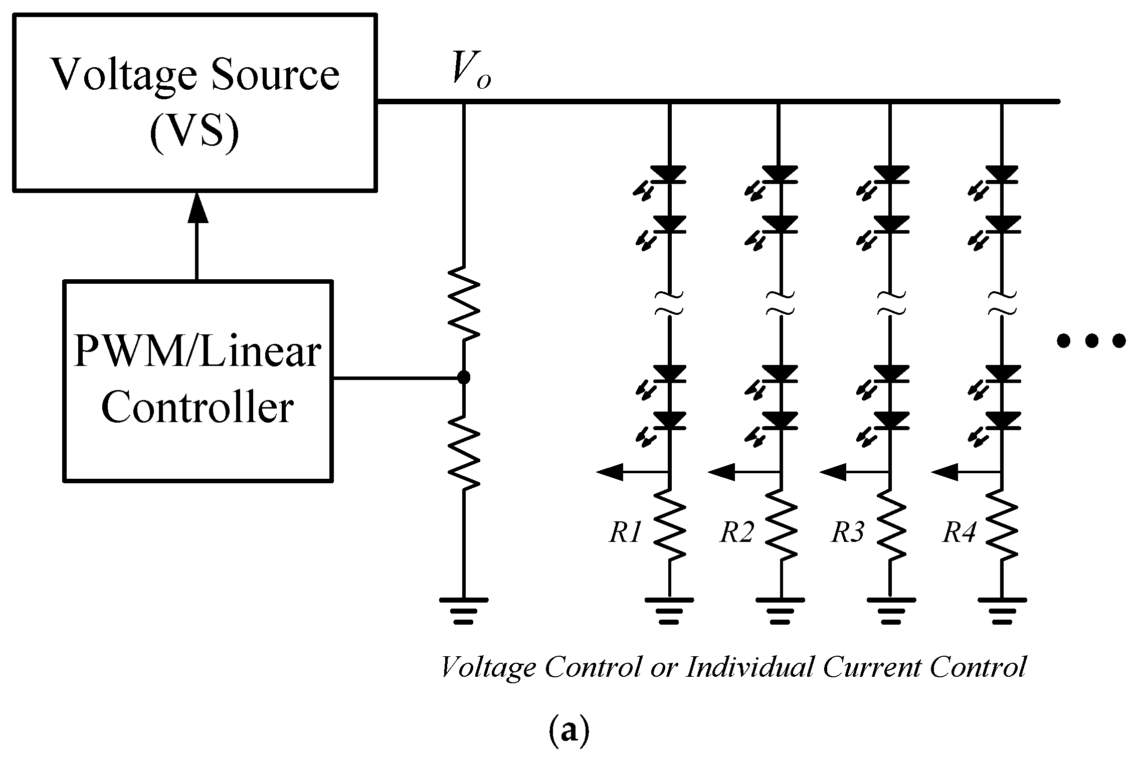
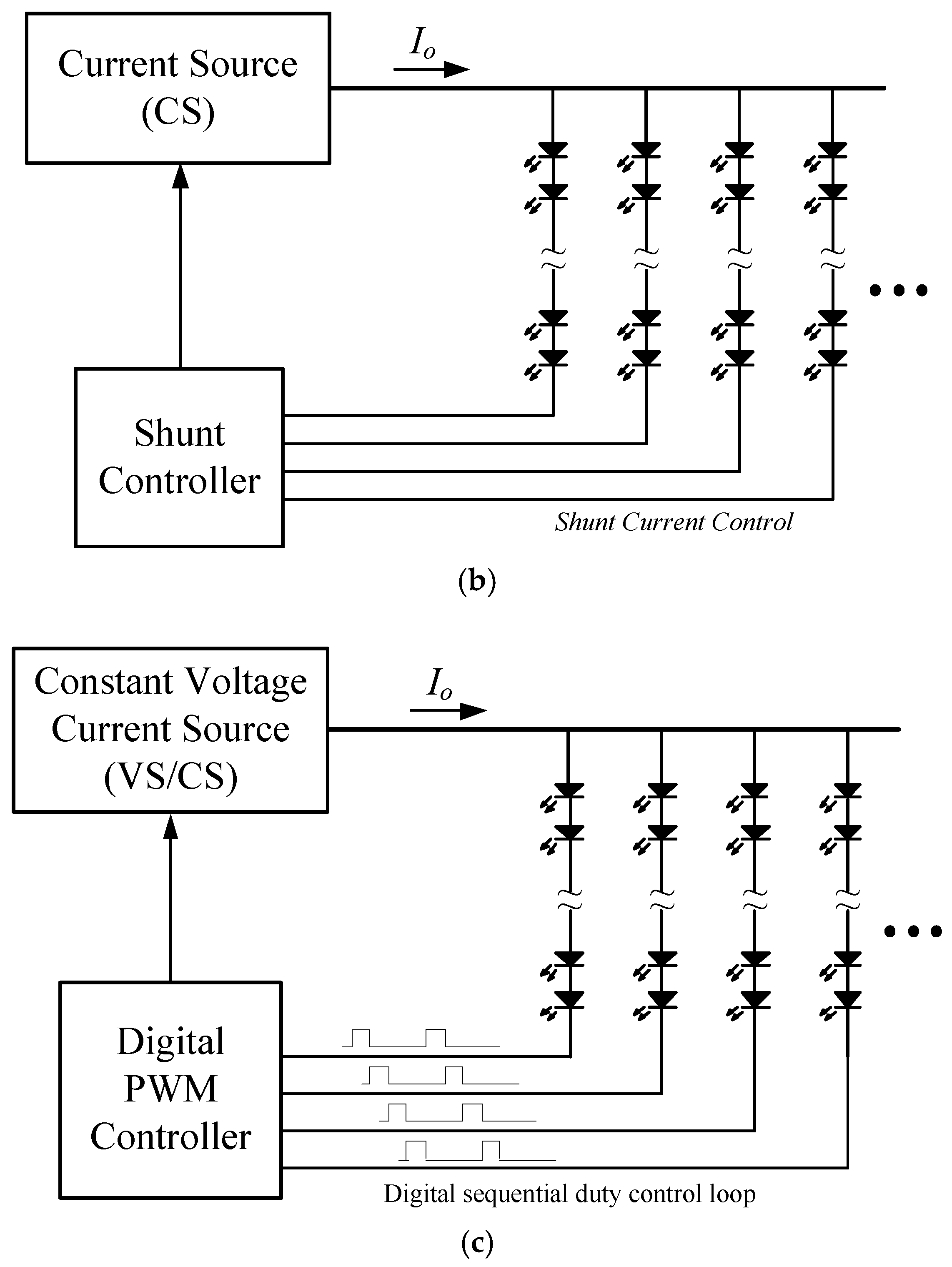
:1. Introduction
2. Aspect of Linear Current Regulator for LEDs
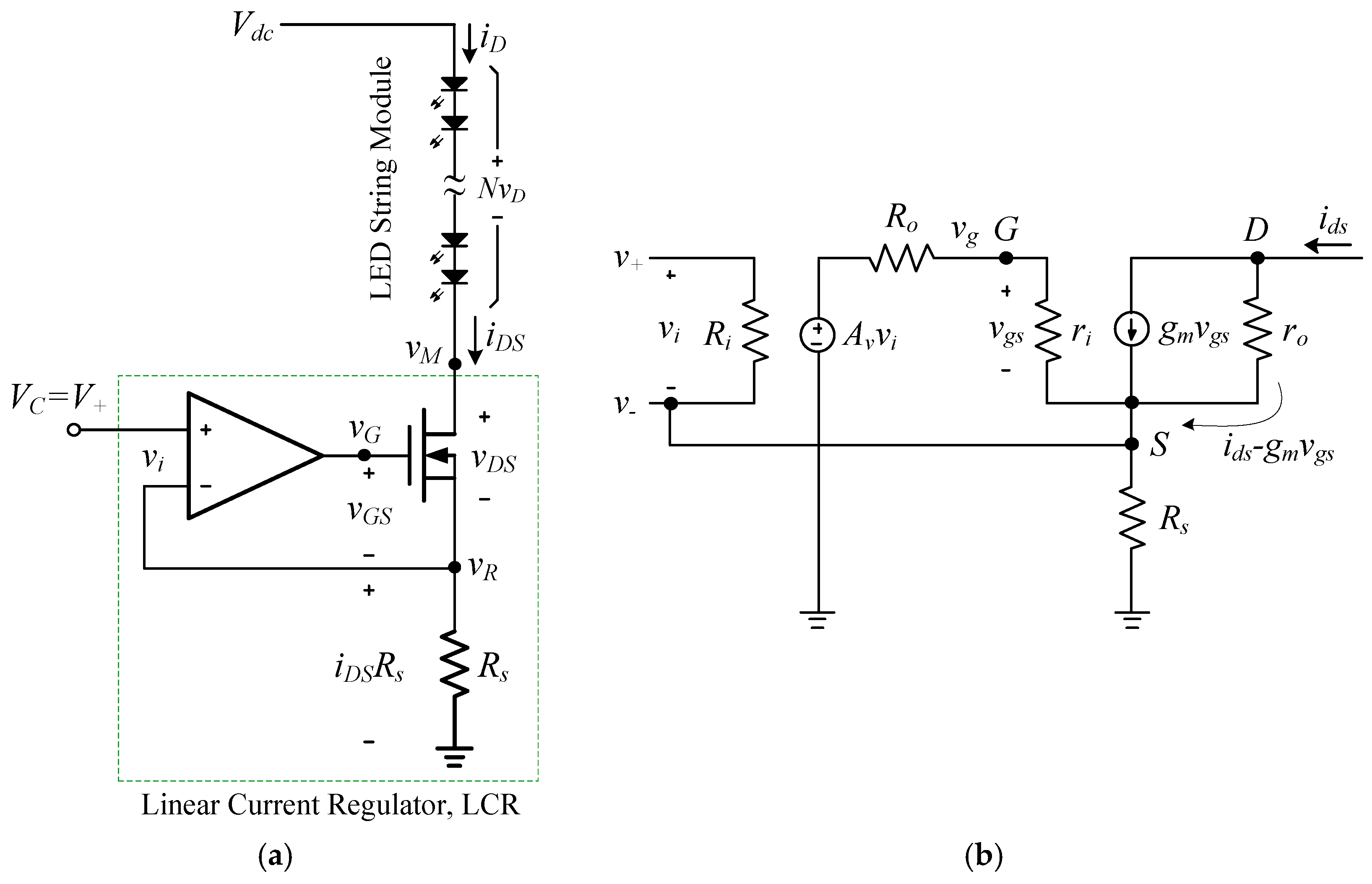
2.1. Linear Current Regulator
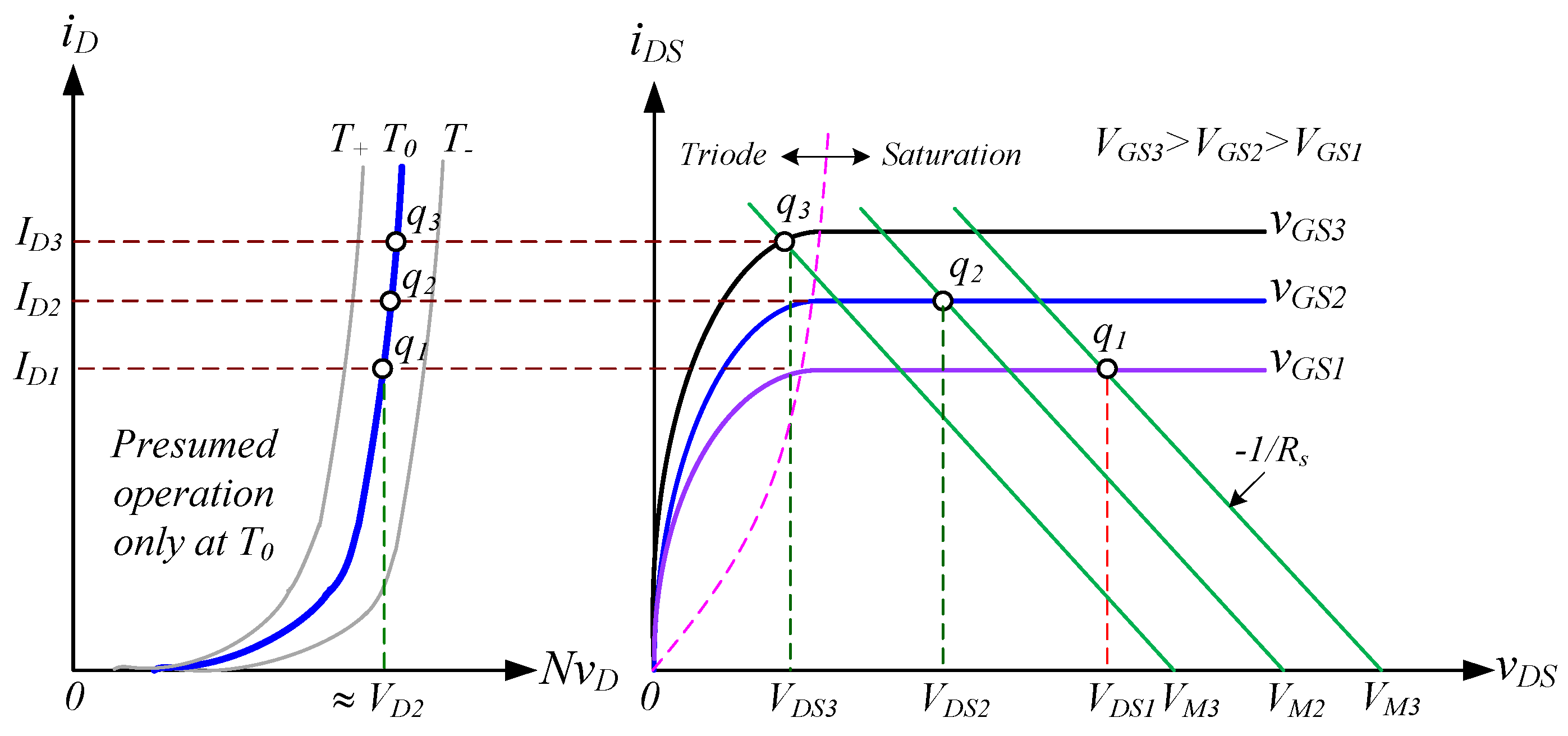
2.2. LED String Module in LCR
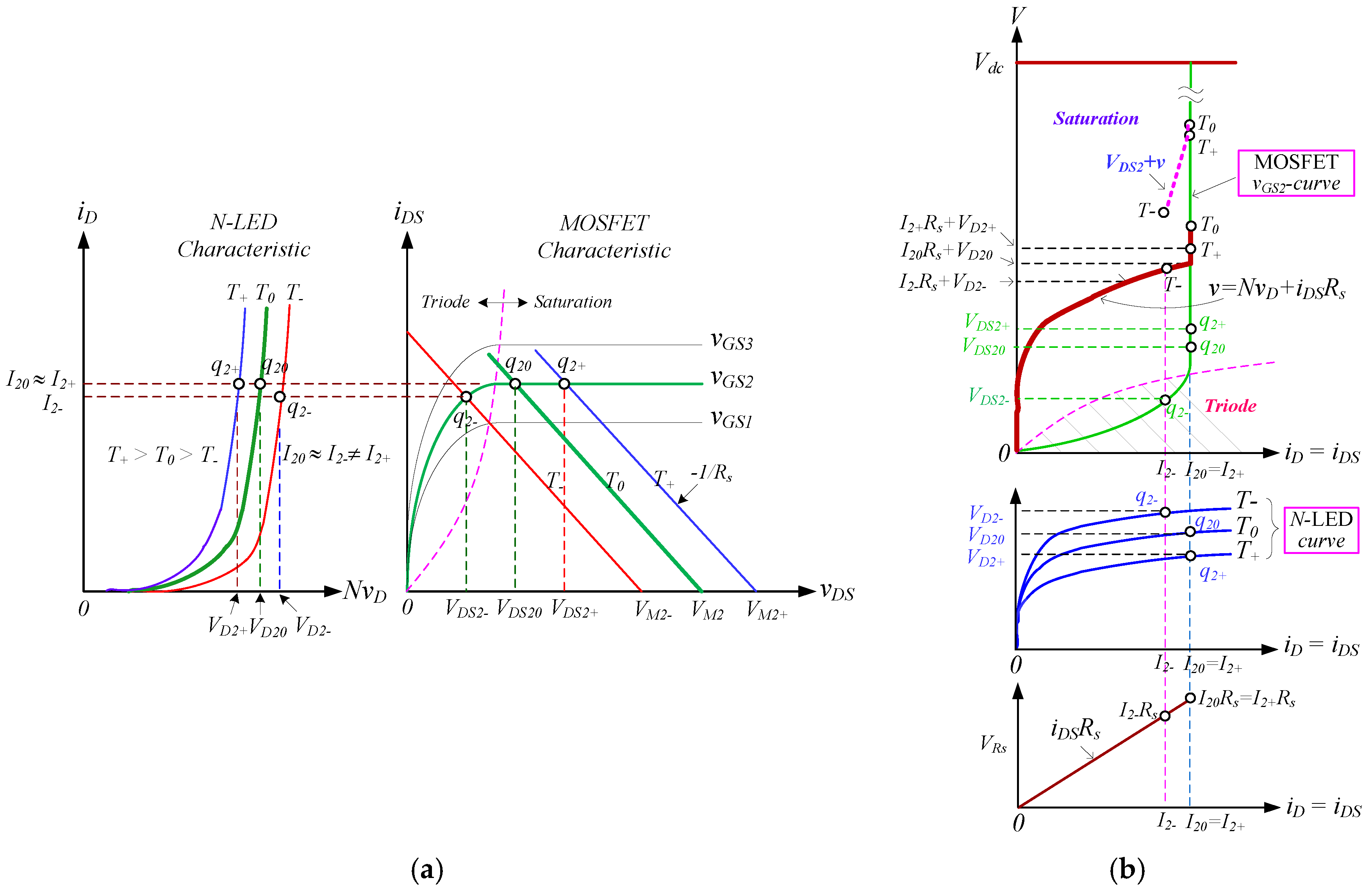
Bias Situation for a Single String LED
2.3. Dimming with a Constant Voltage Supply to LCR
3. Variable Voltage Regulator for LCRs to Balance the String LED Currents
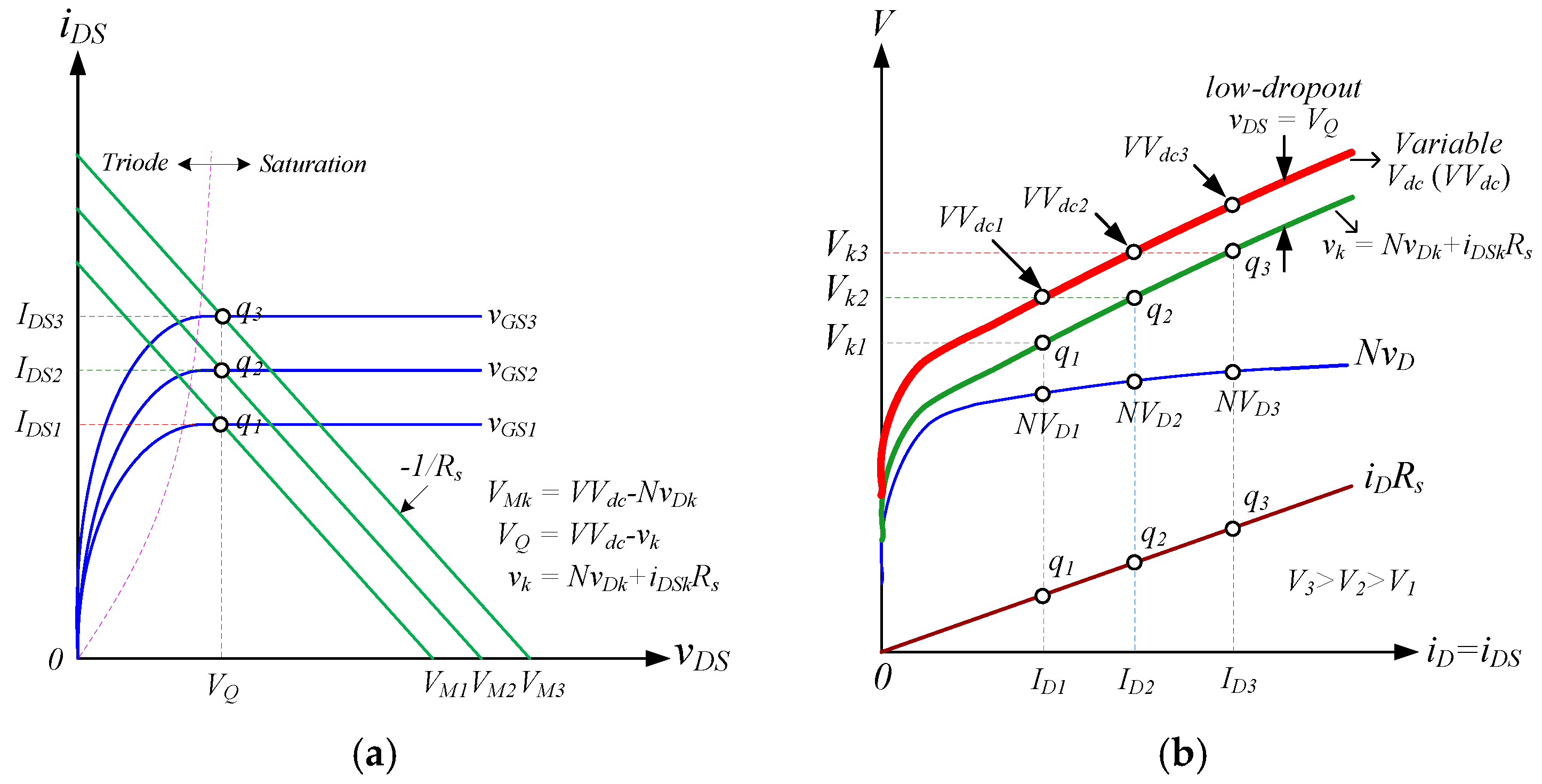
3.1. VVdc Synthesized to Clamp Low-Dropout vDS in the MOSFET
3.2. Dimming for Multiple-String N-LEDs
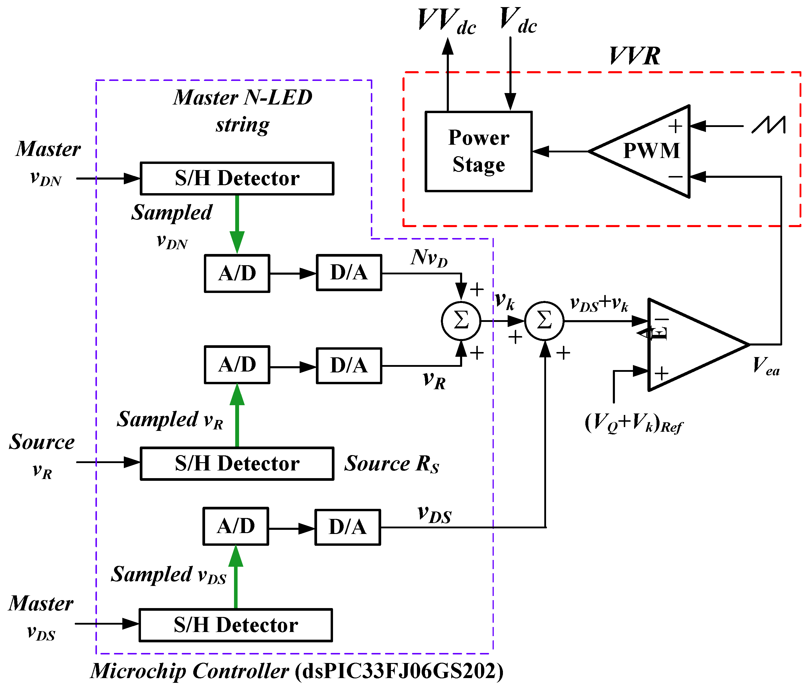
3.3. Master and Slave Control for Current Balance of Multiple string N-LEDs
3.4. Digitizing the VVR Controller
4. Design and Experiment
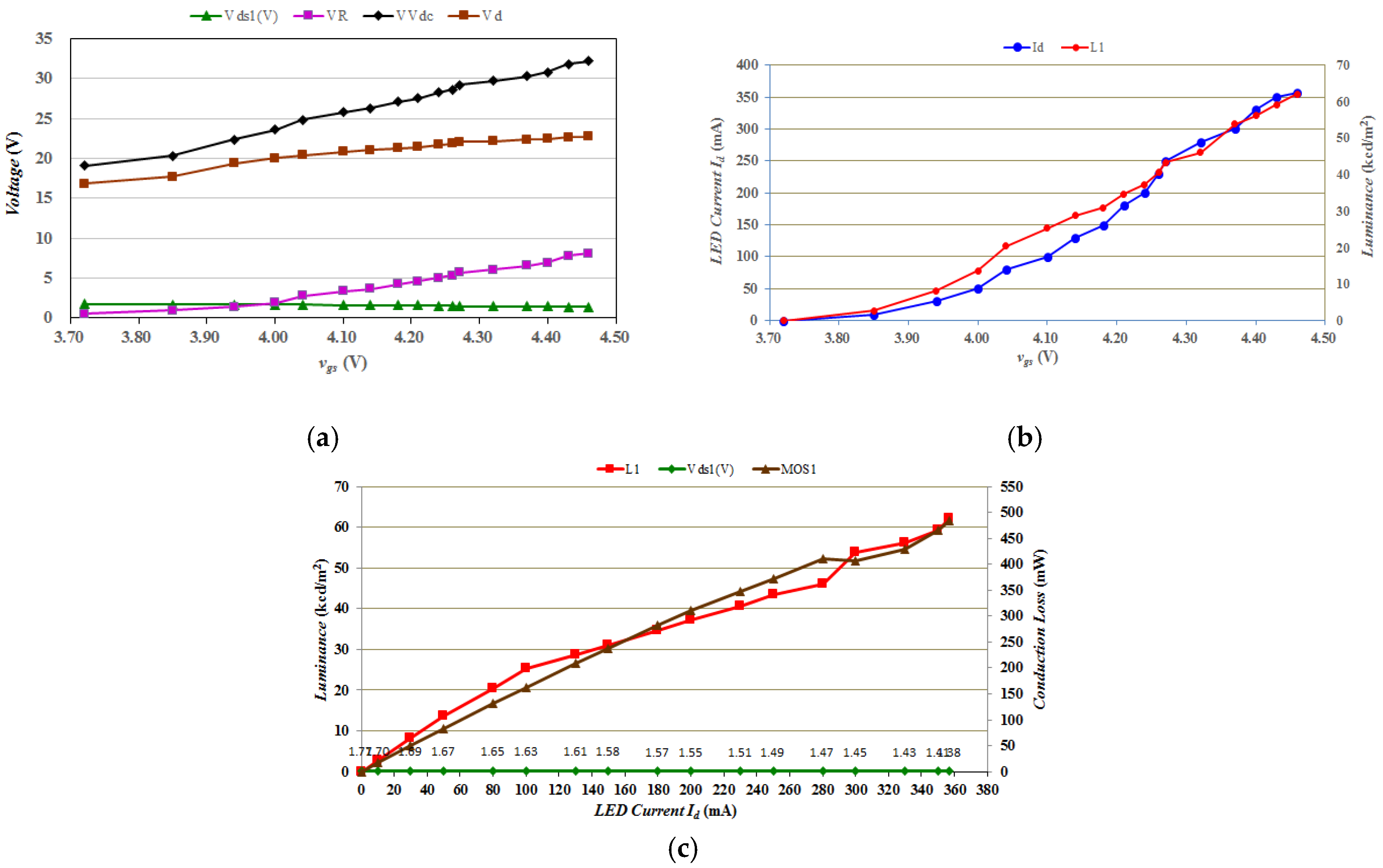
4.1. Experiment for a Single String 6-LED
4.2. Experiment for the Multiple String 6-LEDs
5. Conclusions
Acknowledgments
Author Contributions
Conflicts of Interest
References
- Swanson, D.F.; Criscione, M. LED Driver Circuit and Method. U.S. Patent 6,362,578 B1, 26 March 2002. [Google Scholar]
- Burgyan, L.; Prinz, F. High Efficiency LED Driver. U.S. Patent 6,690,146 B2, 10 February 2004. [Google Scholar]
- Otake, T. Switching Constant-Current Power Supply System. U.S. Patent 7,235,899 B2, 26 June 2007. [Google Scholar]
- Narra, P.; Zinger, D.S. An Effective LED Dimming Approach. In Proceedings of the IEEE Industry Applications Conference, Seattle, WA, USA, 3–7 October 2004.
- Nishikawa, M.; Ishizuka, Y.; Matsuo, H.; Shigematsu, K. An LED Drive Circuit with Constant-Output-Current Control and Constant-Luminance Control. In Proceedings of the International Telecommunications Energy Conference (INTELEC), Providence, RI, USA, 10–14 September 2006.
- Van der Broeck, H.; Sauerlander, G.; Wendt, M. Power Driver Topologies and Control Schemes for LEDs. In Proceedings of the IEEE Applied Power Electronics Conference and Exposition (APEC), Anaheim, CA, USA, 25 February–1 March 2007.
- Garcia, J.; Calleja, A.J.; Corominas, E.L.; Gacio, D.; Campa, L.; Díaz, R.E. Integrated driver for power LEDs. In Proceedings of the IEEE Industrial Electronics Conference (IECON), Glendale, AZ, USA, 7–10 November 2010.
- Chen, H.; Zhang, Y.; Ma, D. A SIMO Parallel-String Driver IC for Dimmable LED Backlighting With Local Bus Voltage Optimization and Single Time-Shared Regulation Loop. IEEE Trans. Power Electron. 2012, 27, 452–462. [Google Scholar] [CrossRef]
- Li, S.N.; Zhong, W.X.; Chen, W.; Hui, S.Y.R. Novel Self-Configurable Current-Mirror Techniques for Reducing Current Imbalance in Parallel Light-Emitting Diode (LED) Strings. IEEE Trans. Power Electron. 2012, 27, 2153–2162. [Google Scholar] [CrossRef] [Green Version]
- Choi, S.; Kim, T. Symmetric Current-Balancing Circuit for LED Backlight with Dimming. IEEE Trans. Ind. Electron. 2012, 59, 1698–1707. [Google Scholar] [CrossRef]
- Choma, J. Temperature Stable Voltage Controlled Current Source. IEEE Trans. Circuits Syst. I Fundam. Theory Appl. 1994, 41, 405–411. [Google Scholar] [CrossRef]
- Doshi, M.; Zane, R. Digital Architecture for Driving Large LED Arrays with Dynamic Bus Voltage Regulation and Phase Shifted PWM. In Proceedings of the IEEE Applied Power Electronics Conference and Exposition (APEC), Anaheim, CA, USA, 25 February–1 March 2007.
- Chiu, H.J.; Lo, Y.K.; Chen, J.T.; Cheng, S.J.; Lin, C.Y.; Mou, S.C. A High-Efficiency Dimmable LED Driver for Low-Power Lighting Application. IEEE Trans. Ind. Electron. 2010, 57, 735–743. [Google Scholar] [CrossRef]
- Chiu, H.J.; Cheng, S.J. LED Backlight Driving System for Large-Scale LCD Panels. IEEE Trans. Ind. Electron. 2007, 54, 2751–2760. [Google Scholar] [CrossRef]
- Oh, I.H. An Analysis of Current Accuracies in Peak and Hysteretic Current Controlled Power LED Drivers. In Proceedings of the IEEE Applied Power Electronics Conference and Exposition (APEC), Austin, TX, USA, 24–28 February 2008.
- Hu, Y.; Jovanovic, M.M. LED Driver with Self-Adaptive Drive Voltage. IEEE Trans. Power Electron. 2008, 23, 3116–3125. [Google Scholar] [CrossRef]
- Hu, Q.; Zane, R. LED Driver Circuit with Series-Input-Connected Converter Cells Operating in Continuous Conduction Mode. IEEE Trans. Power Electron. 2008, 25, 574–582. [Google Scholar]
- Zhang, R.; Chung, H.S.H. Paralleled LED Strings—An Overview of Current Balancing Techniques. IEEE Ind. Electron. Mag. 2015, 9, 17–23. [Google Scholar] [CrossRef]
- Sedra, A.S.; Smith, K.C. Microelectronic Circuits, 7th ed.; Oxford University Press: New York, NY, USA, 2016; pp. 174–230. [Google Scholar]
- Lin, Y.L.; Chiu, H.J.; Lo, Y.K.; Leng, C.M. Light-Emitting Diode Driver with a Combined Energy Transfer Inductor for Current Balancing Control. IET Power Electron. 2015, 8, 1834–1843. [Google Scholar] [CrossRef]
- Gacio, D.; Alonso, J.M.; Garcia, J.; Garcia-Llera, D.; Cardesín, J. Study on Passive Self-Equalization of Parallel-Connected LED Strings. IEEE Trans. Ind. Appl. 2015, 51, 2536–2543. [Google Scholar] [CrossRef]
- Ye, Y.; Cheng, K.W.E.; Lin, J.; Wang, D. Single-Switch Multichannel Current-Balancing LED Drive Circuits Based on Optimized SC Techniques. IEEE Ind. Electron. 2015, 62, 4761–4768. [Google Scholar] [CrossRef]
- Wu, X.; Hu, C.; Zhang, J.; Qian, Z. Analysis and Design Considerations of LLCC Resonant Multioutput DC/DC LED Driver with Charge Balancing and Exchanging of Secondary Series Resonant Capacitors. IEEE Trans. Power Electron. 2015, 30, 780–789. [Google Scholar] [CrossRef]
- Chen, X.; Huang, D.; Li, Q.; Lee, F.C. Multichannel LED Driver with CLL Resonant Converter. IEEE J. Emerg. Sel. Top. Power Electron. 2015, 3, 589–598. [Google Scholar] [CrossRef]
- Hwu, K.I.; Jiang, W.Z. Nonisolated Two-Channel LED Driver with Automatic Current Balance and Zero-Voltage Switching. IEEE Trans. Power Electron. 2016, 31, 8359–8370. [Google Scholar] [CrossRef]
- Hsieh, H.I.; Peng, S.W.; Cheng, J.T. Low-Dropout Voltage Regulator for Stabilizing LEDs Drives in Dimmable Group Current Sinks. In Proceedings of the IEEE Applied Power Electronics Conference and Exposition (APEC), Fort Worth, TX, USA, 6–11 March 2011.


© 2017 by the authors. Licensee MDPI, Basel, Switzerland. This article is an open access article distributed under the terms and conditions of the Creative Commons Attribution (CC BY) license ( http://creativecommons.org/licenses/by/4.0/).
Share and Cite
Hsieh, H.-I.; Wang, H. LED Current Balance Using a Variable Voltage Regulator with Low Dropout vDS Control. Appl. Sci. 2017, 7, 206. https://0-doi-org.brum.beds.ac.uk/10.3390/app7020206
Hsieh H-I, Wang H. LED Current Balance Using a Variable Voltage Regulator with Low Dropout vDS Control. Applied Sciences. 2017; 7(2):206. https://0-doi-org.brum.beds.ac.uk/10.3390/app7020206
Chicago/Turabian StyleHsieh, Hung-I, and Hao Wang. 2017. "LED Current Balance Using a Variable Voltage Regulator with Low Dropout vDS Control" Applied Sciences 7, no. 2: 206. https://0-doi-org.brum.beds.ac.uk/10.3390/app7020206