
Comparison of Light Trapping in Silicon Nanowire and Surface Textured Thin-Film Solar Cells

Jacobs University Bremen, 28759 Bremen, Germany
*
Author to whom correspondence should be addressed.
†
Present address: University of California Observatories, Santa Cruz, CA 95064, USA.
‡
Present address: Stanford University, Stanford, CA 94305, USA.
Appl. Sci. 2017, 7(4), 427; https://0-doi-org.brum.beds.ac.uk/10.3390/app7040427
Submission received: 6 March 2017
/
Revised: 17 April 2017
/
Accepted: 18 April 2017
/
Published: 24 April 2017
(This article belongs to the Special Issue Light Management for Optoelectronics)
Abstract
:The optics of axial silicon nanowire solar cells is investigated and compared to silicon thin-film solar cells with textured contact layers. The quantum efficiency and short circuit current density are calculated taking a device geometry into account, which can be fabricated by using standard semiconductor processing. The solar cells with textured absorber and textured contact layers provide a gain of short circuit current density of 4.4 mA/cm2 and 6.1 mA/cm2 compared to a solar cell on a flat substrate, respectively. The influence of the device dimensions on the quantum efficiency and short circuit current density will be discussed.
1. Introduction
Efficient light management techniques are necessary for increasing the short circuit current density and quantum efficiency of silicon thin-film solar cells [1]. Experimentally, high conversion efficiencies have been achieved by texturing the contact layers of silicon solar cells [2,3,4,5,6,7,8,9]. The nanotextured contact layers reduce reflection losses and enhance the scattering and diffraction of light within the solar cells. Moreover, the optical path length is increased leading to an enhanced quantum efficiency and short circuit current density in the red and infrared range of the optical spectrum (wavelengths between 600 and 1100 nm) [6,7,8,9]. Furthermore, alternative approaches, such as 3D solar cells [10,11,12,13,14,15] or nanowire solar cells, have gained considerable attention in recent years [16,17,18,19,20]. Axial nanowire solar cells are based on the texturing of the active layer of the solar cell instead of texturing the contact layers. Several studies suggest that such nanowire solar cells exhibit very good light trapping properties [10,16,17,18,19,20]. In this study, solar cells with textured contact layers and solar cells with textured absorber are compared taking realistic device structures into consideration. Solar cells on flat substrates are used as reference solar cells.
The optical simulations of the microcrystalline silicon thin-film solar cells on flat substrates are described in Section 2.1. Results for solar cells with textured absorber are presented in Section 2.2. The optical simulations for solar cells with textured contact layers are presented in Section 2.3. A comparison of the different structures is given in Section 3, before providing an outlook and a summary of the results in Section 4 and Section 5.
2. Optics of Microcrystalline Silicon Solar Cells
To describe the wave propagation in silicon thin-film solar cells, simple geometric or wave optics is insufficient. Instead, it is necessary to rigorously solve Maxwell’s equations. Currently, there are a number of methods being utilized such as the finite-difference time-domain (FDTD) method [21], finite integration method (FIM) [22] or Rigorous Coupled Wave Analysis (RCWA) [23] capable of simulating near- and far-field wave propagation in such devices. For this study, a FDTD simulation tool is used to investigate the wave propagation within solar cell structures [24].
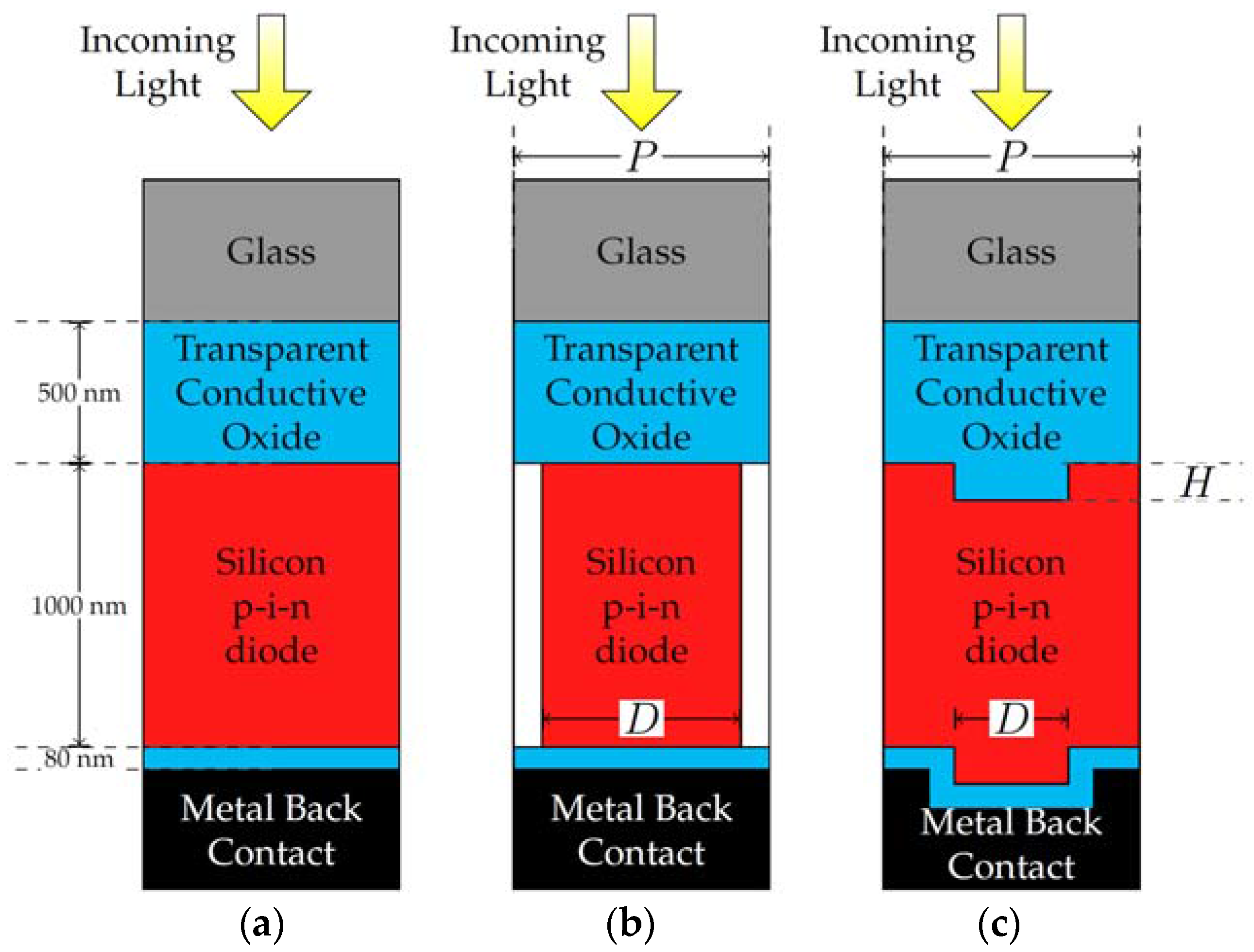
The schematic cross-sections of microcrystalline silicon (μc-Si:H) solar cells in superstrate configuration are depicted in Figure 1. A solar cell on a flat substrate is shown in Figure 1a. Cross-sections of solar cells with textured contacts and absorber layer are shown in Figure 1b,c, respectively. The cross section in Figure 1b,c shows a slice through the center of a 3D unit cell. All three solar cell structures follow the same basic layer sequence with: a 500 nm thick sputtered aluminum doped zinc oxide (ZnO:Al) front contact, followed by a μc-Si:H p-i-n diode with a total thickness of 1000 nm, a back reflector consisting of 80 nm thick ZnO:Al, and a perfect electrical conductor (PEC, 100% reflection) terminating the stack. The layer sequence used for the simulations is consistent with structures used in the literature [4,6]. The thickness of the ZnO:Al front contact layer is consistent with reference solar cells prepared on flat substrates [4,6]. The thickness of the p-layer of p-i-n diode is assumed to be 30 nm, while the n-layer of the p-i-n diode has a thickness of 10 nm. In order to realize a solar cell with textured absorber, the p-i-n diode is patterned, while, in the case of a solar cell with textured contacts, only the front contact is textured. Subsequently, the p-i-n layer stack and back contact of the solar cell with textured contacts are formed on the front contact. The morphology of the p-i-n layer stack and back contact follows the front contact morphology. Hence, all layers of the solar cell are textured. However, in the following the structure is named solar cell with textured contact layers to point out that only the front contact layer is intentionally textured during the fabrication process. The subsequently formed p-i-n layer stack is unintentionally textured. The texturing of the p-i-n layer stack is the consequence of preparing the layers on a textured substrate.
The optical constants of the μc-Si:H material and the ZnO:Al film are adapted from the literature [4].
As the first step of the FDTD optical simulations, the electrical field distribution is calculated for a unit solar cell structure assuming normal incidence light with an electric field amplitude of 1 V/m. Based on the electric field distribution, the time-averaged power loss (Q(x,y,z)) is determined within the solar cell via the equation:
where c is the speed of light in free space, ε0 is the permittivity of free space, α is the absorption coefficient of the material at the given position, n is the real part of the complex refractive index, and E(x,y,z) is the electric field. The absorption coefficient is calculated by α(λ) = 4πk/λ, where λ is the wavelength and k is the imaginary part of the complex refractive index. The absorption of light by the individual layer of the solar cell is defined as the ratio of the power absorbed by the layer with respect to the total power incident, Popt, on the unit cell. The absorption of the m-th layer of the solar cell is given by
where Vm is the volume of the m-th layer. The quantum efficiency is given by
where Ai-layer is the absorption of the i-layer of the p-i-n diode and CE(λ) is the wavelength dependent collection efficiency. The collection efficiency of the i-layer of the solar cell is assumed to be 100%, thus defining an upper limit on the achievable quantum efficiency. Light absorbed by the front contact, back reflector, p-layer and n-layer does not contribute to the quantum efficiency. In order to compare the different device designs, the short circuit current density is calculated for the three regions of the optical spectrum (blue: 300–500 nm, green: 500–700 nm, and red: 700–1100 nm). The short circuit current density is calculated from the quantum efficiency by
with
where, q is the elementary charge, h is the Planck constant and S(λ) is the spectral irradiance at Air Mass 1.5.
2.1. Solar Cell on Flat Substrates
The reference solar cell on a flat substrate (Figure 1a) exhibits a short circuit current density of 12.4 mA/cm2. The corresponding quantum efficiency is shown in Figure 3a,b (black curve). Due to silicon’s strong absorption at short wavelengths, light is absorbed within the first few hundreds of nanometers of the solar cell. At long wavelengths, the absorption coefficient is much weaker, so a large fraction of light is able to pass through the silicon layer and is reflected by the back contact. This leads to the constructive and destructive interferences of the forward and backward propagating waves and the formation of interference peaks in the quantum efficiency. Only a fraction of the incident light is absorbed, which limits the quantum efficiency. Therefore, one of the primary ways to achieve improved performance of microcrystalline silicon solar cells at long wavelengths is to introduce improved light management techniques.
2.2. Solar Cells with Textured Silicon Absorbers
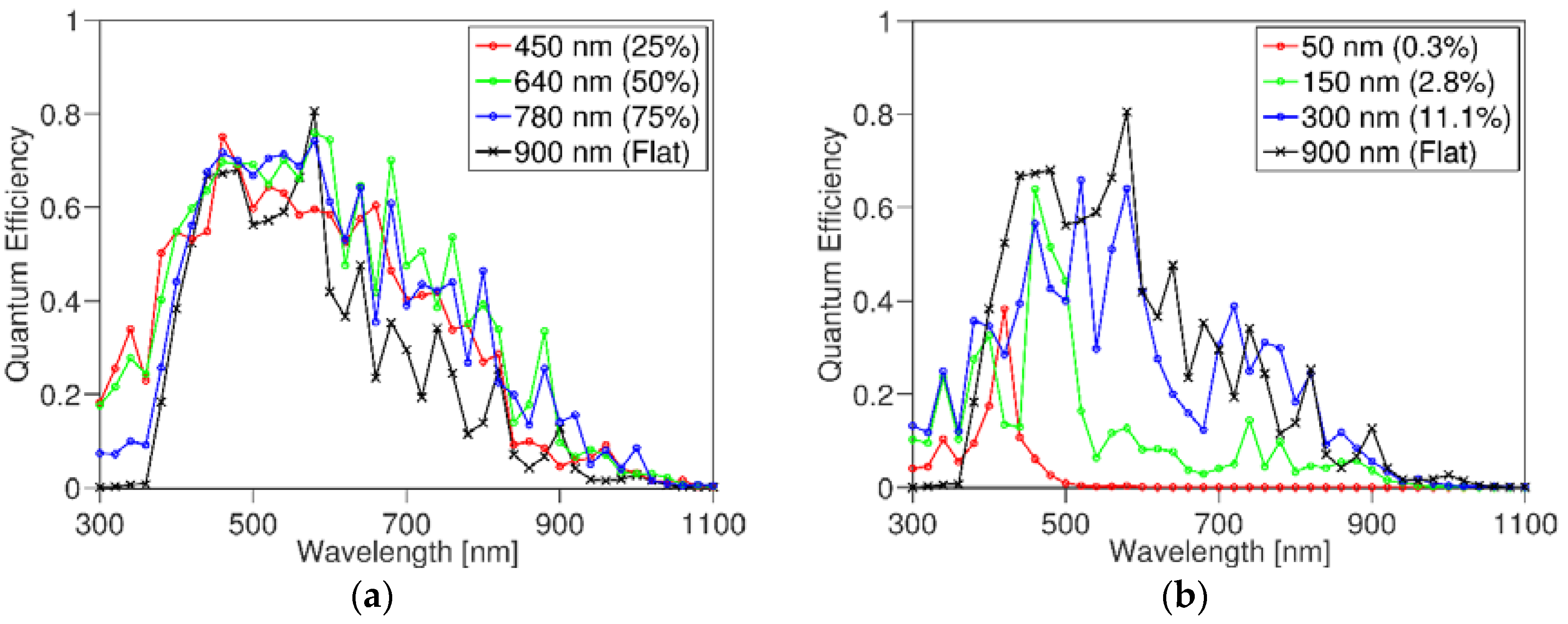
The optical model used in this study is based on a periodic arrangement of silicon nanowires. The array of nanowires represents a solar cell with a patterned absorber. The dimensions of the nanowire solar cell are described by the period of the unit cell, P, and the diameter of the nanowire, D (Figure 1b). The nanowire is square-based, so the term “diameter” is equivalent to the edge-length of the nanowire. The area filling factor of the nanowire is equal to (D/P)2. A constant unit cell period of 900 nm is chosen for these simulations as previous studies have shown that the optimal period of the surface texture is approximately equal to the thickness of the solar cell [9]. The diameter of the nanowire is varied from 50 nm to 900 nm corresponding to area fill factors ranging from 0.3% to 100%. In other words, the area filled with air is varied from 0% to 99.7%.
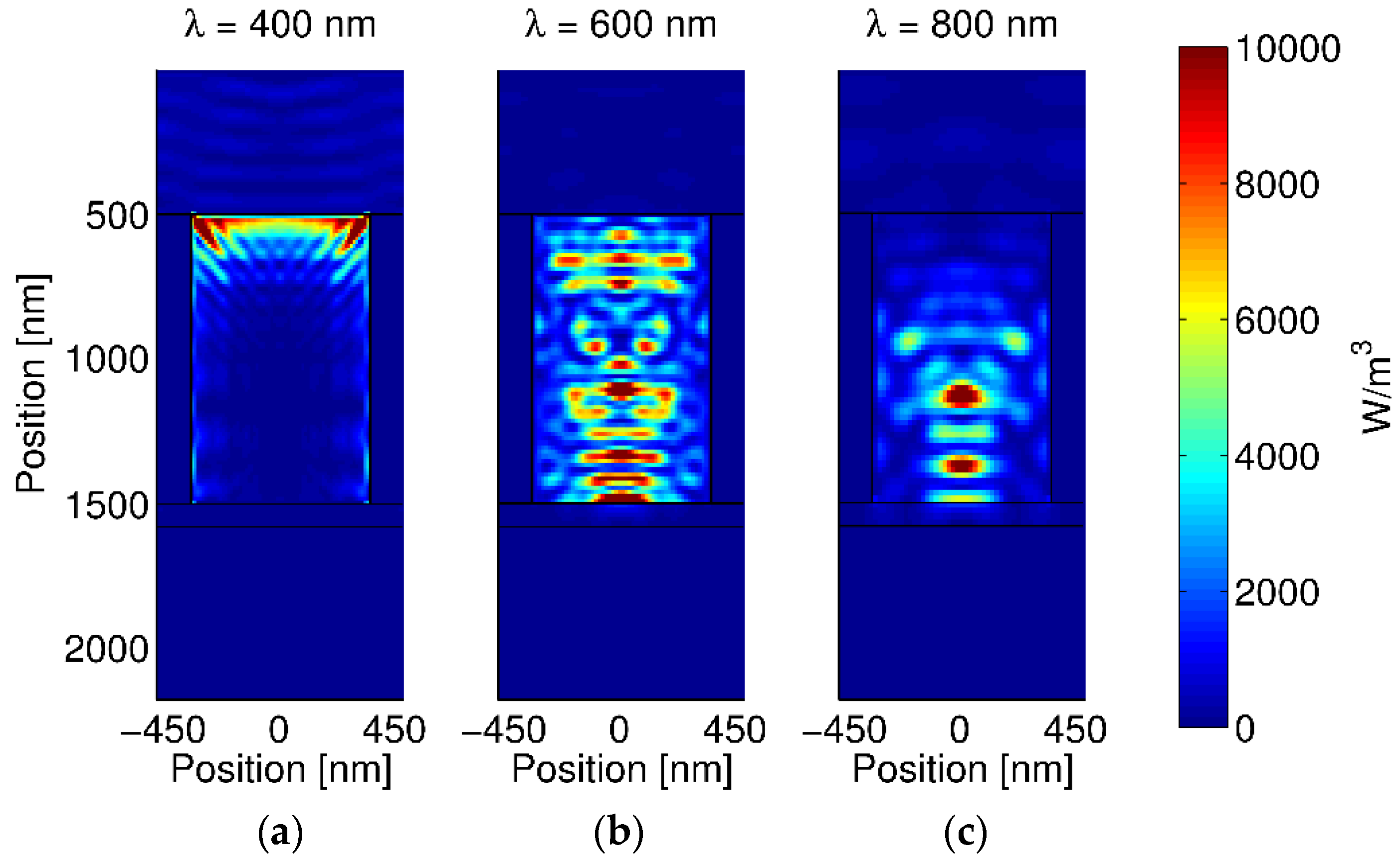
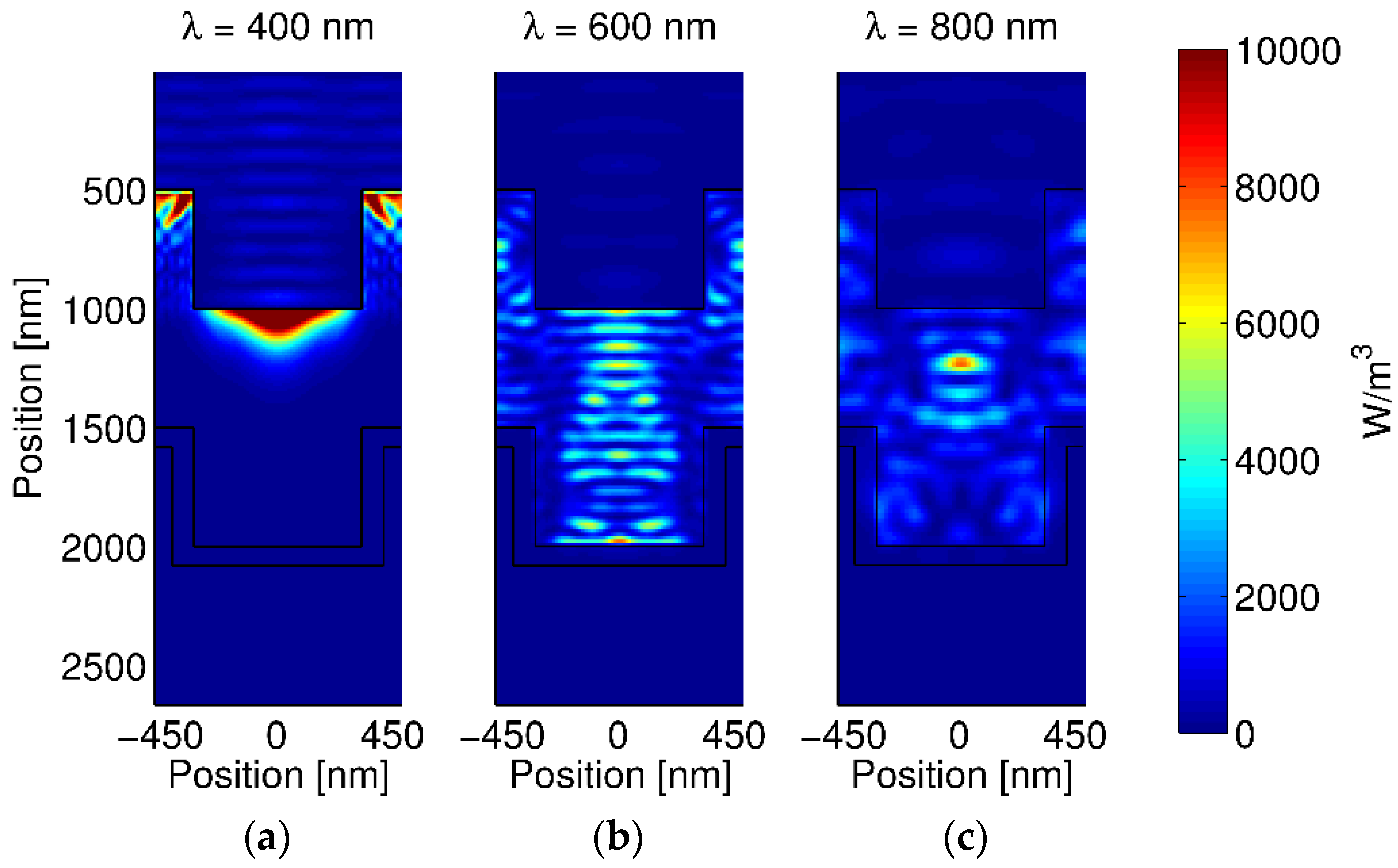
The simulated power loss profiles for a solar cell with textured absorber are shown in Figure 2a–c for incident wavelengths of 400 nm, 600 nm and 800 nm, respectively. These power loss profiles are shown for a diameter of 640 nm and period of 900 nm. For short wavelengths, absorption of light is most prominent along the front surface and edges of the absorber layer. The edges of the silicon nanowires show strong absorption since the light propagates in the gaps between nanowires. The light that is absorbed by the edges lead to an increased quantum efficiency in the spectral range from 300 to 380 nm. The quantum efficiency in this spectral region is increased because the sidewalls are not covered with a p- or n-layer. For long wavelengths, the absorption and quantum efficiency of light in the solar cell is enhanced (Figure 3a). The long wavelength light is diffracted by the silicon nanowire. It is important to note that the simulations are carried out in 3D and hence, the light is diffracted in all three dimensions. In the case of 2D simulations the nanowire array would be replaced by a line grating and the light would only by diffracted in 2D. The 3D diffraction grating (nanowire array) leads to a higher quantum efficiency and short circuit current density compared to 2D diffraction gratings (line grating).
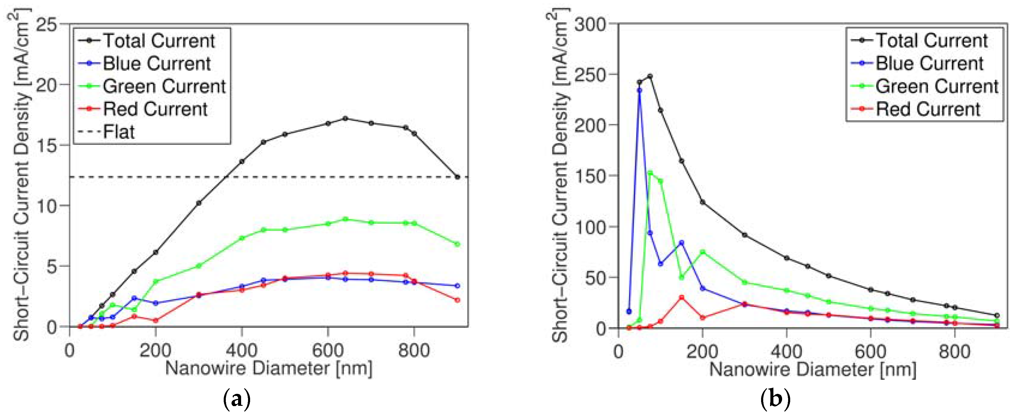
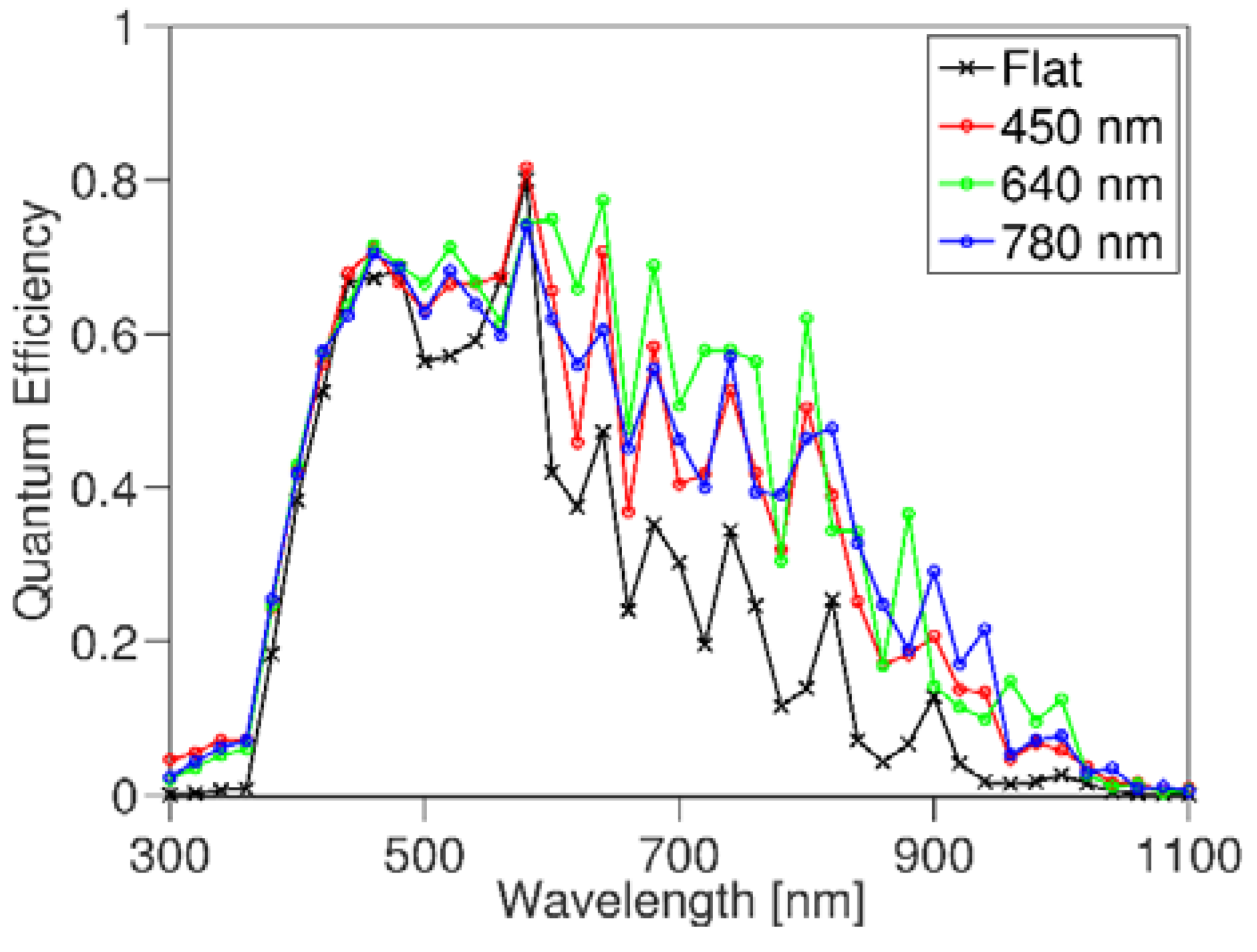
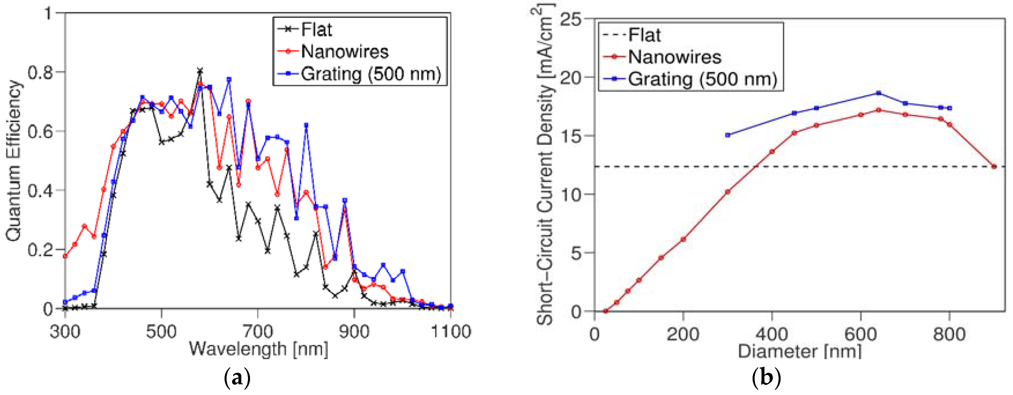
For nanowire diameters larger than 640 nm a drop of the quantum efficiency for long wavelengths is observed (Figure 3a). Figure 4a shows the red, green, blue and total short circuit current densities for nanowires with a constant period of 900 nm and varying diameter. The dashed line exhibits the short circuit current density generated by a solar cell on a flat substrate. For the flat substrate (Figure 1a), a total short circuit current density of 12.4 mA/cm2 is calculated. For the silicon nanowire solar cell (Figure 1b) with a nanowire diameter between 400 and 900 nm, an improvement of short circuit current density over the flat substrate is achieved, with optimal performance at nanowire diameter of 640 nm. At this optimal diameter, the short circuit current density is found to be 16.8 mA/cm2 (Figure 4a). For diameters of the nanowire smaller than 400 nm, the total short circuit current density drops below the short circuit current density of a solar cell on a flat substrate (Figure 4a). With decreasing diameter, long wavelengths light cannot couple in the nanowires anymore (Figure 3b). The cut-off wavelength for coupling light in the wire is given by
where nSi is the refractive index of the silicon wire. For nanowires with diameters smaller than 135 nm, the quantum efficiency is limited by the incoupling of long wavelength light in the nanowire. Hence, the short circuit current density drops with decreasing diameter of the nanowire. However, if the short circuit current is normalized to the cross section of the nanowire instead of normalizing to the area of the unit cell the short circuit current density increases to up to 250 mA/cm2 (Figure 4b). Such high short circuit densities are observed for nanowires with diameters of 50 nm and 75 nm. For nanowires with very small diameters even a drop of the short circuit current normalized to the cross section of the nanowire is observed. For a nanowire diameter of 30 nm, the short circuit current density drops to almost zero. The nanowire diameter is too small to allow for the coupling of light (300–1100 nm) in the nanowire.
In this study, perfectly periodic and uniform unit cell structures are assumed. Introducing imperfections and non-uniformities can be expected when experimentally realizing the structure. As an alternative such imperfections or non-uniformities can be introduced intentionally. For example, the influence of randomness has been intensively studied for solar cells with randomly textured contact layers. Some of these results can be transferred to solar cells consisting of randomly arranged nanowires. However, it is important to distinguish between nanowires with diameters significantly larger than the optical wavelength and nanowires with diameters smaller than the optical wavelengths. For randomly arranged nanowires with large diameters, the quantum efficiency can be approximated by the superposition of periodic structures with different period [5]. Small changes of the diameter of the nanowires have only a small effect on the quantum efficiency. For nanowires with small diameters the situation is different. In the latter case, the quantum efficiency is determined by the optical resonance of each individual nanowire. The density of the nanowires determines the absolute value of the quantum efficiency. Changes of the diameter lead to a broadening of the quantum efficiency and an increased absolute value of the quantum efficiency.
2.3. Solar Cells with Textured Contact Layers
The solar cell structure shown in Figure 1c is based on a periodic arrangement of square-based ZnO:Al nanopatterned pillars on a continious ZnO:Al film or a 2D grating structure. The surface texture is described by the following key parameters: cell period (P), grating diameter (D) and grating height (H). The p-i-n diode and the back contact are formed on the textured front contact. Consequently, all layers of the solar cell are textured. In this study, only the influence of the grating diameter on the quantum efficiency is investigated. Grating diameters ranging from 300 to 800 nm are considered, while the height of the grating is kept constant at 500 nm. Figure 5a–c show the power loss profiles for a diameter of 640 nm at wavelengths of 400 nm, 600 nm and 800 nm, respectively. An enhanced absorption of the solar cell is observed for all three wavelengths.
The quantum efficiency for grating diameters of 450 nm, 640 nm and 780 nm is shown in Figure 6. The highest short circuit current density of 18.5 mA/cm2 is observed for a diameter of 640 nm, corresponding to a 50% area filling factor. An enhancement of the quantum efficiency is negligible for short wavelengths, while a distinct improvement on the quantum efficiency is observed for long wavelengths (>500 nm) compared to solar cell on a flat substrate. Furthermore, a gain of the short circuit current densities is observed for grating diameters ranging from 300 to 800 nm, with the highest short circuit current density at a diameter of 640 nm. For large and small diameters, the short circuit current densities converges towards that of solar cell on a flat substrate (Figure 1a) as shown in Figure 7b.
3. Comparison of Contact and Absorber Textured Solar Cells
The quantum efficiency of optimized solar cells with textured contact layer and absorber, and a solar cell on a flat substrate are shown in Figure 7. Both textured solar cells exhibit an enhanced quantum efficiency (Figure 7a), and a gain in the short circuit current density compared to a solar cell on a flat substrate (Figure 7b). At short wavelengths (300–380 nm), the solar cells with textured absorber exhibit a higher quantum efficiency compared to solar cells with textured contacts and flat substrate. As a result, a gain in the blue short circuit current density for the nanowires based solar cells is observed. However, for long wavelengths the solar cells with textured contact exhibit a higher quantum efficiency compared to solar cells with textured (Figure 7a) absorber. Hence, the total circuit current densities of the solar cells with textured contact layers exceed the short circuit current density of the solar cell with flat substrate and textured absorber (Figure 7b).
However, due to the increased short circuit to saturation current density ratio, the open circuit voltage of the solar cell using textured absorber might be increased compared to the solar cell with textured contact layers [25,26]. The open circuit voltage of the solar cell on the flat substrate is given by
where η is the ideality factor, k is the Boltzmann constant, T is the absolute temperature, and q is the elementary charge. ISC and IS are the short circuit and saturation current densities, respectively. If we assume equal ideality factors for the solar cell with patterned absorbers and flat substrate, the open circuit voltage of the patterned absorber solar cell can be calculated accordingly. The saturation current density of the nanowire solar cell can be described by ISNW = ISflat × (D/P)2 leading to a significant drop of the saturation current density as function of the nanowire diameter. The relationship between the short circuit current density of the nanowire solar cell and the flat solar cell can be approximated by ISCNW ≈ ISCflat × (D − Dcut)/(P/2), where Dcut is the diameter of the nanowire at which no sun light is able couple in the nanowire anymore. Dcut is calculated to be 30 nm (Figure 4a). This relationship represents an empirical approximation of the short circuit current density, which is valid for Dcut < D < P/2. Hence, the following expression for the open circuit voltage of the solar cell with the textured absorber can be calculated:
For a nanowire diameter of 50 nm the gain of the open circuit voltage is larger than 100 mV. For a nanowire diameter of 400 nm the short circuit current density of the textured absorber is equal to the short circuit current density of the flat solar cell and the gain of the open circuit voltage is approximately equal to 60 mV. By using arrays of nanowires with different diameters broadband absorption can be reached, so that the quantum efficiency and short circuit current density are increased [25]. Hence, larger gains of the open circuit voltage can be achieved. However, the optimization of such nanowire arrays is complex. Optical simulations are imperative in optimizing such device structures.
Furthermore, texturing the absorber of the solar cell allows for the realization of a solar cell with a flat metal back reflector. In the current study, the influence of the back reflector on the quantum efficiency and short circuit current density is not considered. A perfect electrical conductor is used as a back reflector. Replacing the perfect electrical conductor by a commonly used silver reflector will have almost no influence on the quantum efficiency and short circuit current density. A very small drop of both parameters will be observed. However, the situation is different for the solar cell with textured contact layers [27,28,29,30,31,32,33,34,35]. The formation of surface plasmon polaritons and localized plasmon polaritons can lead to a distinct drop of the quantum efficiency for long wavelengths. Detailed experimental and simulation studies have shown that the loss can account for up to 30% of the total short circuit current density [27]. The optical losses increase with increasing roughness of the back contact and decreasing thickness of the solar cell [30,31,32,33]. The optical losses are most sensitive to metal textures with dimensions ranging from 30 to 100 nm [33,35]. The optical losses can be reduced, but not prevented by inserting a dielectric layer with a low refractive index between the metal back reflector and the silicon solar cell [3,4,6,27,35]. In the current study, and in most studies in the literature, a sputtered metal oxide film, e.g., zinc oxide, is inserted between the metal back reflector and the silicon solar cell. The zinc oxide layer lowers the refractive index from approximately 4 for microcrystalline silicon to 2 for sputtered zinc oxide. Decreasing the refractive index leads to a shift of the plasmon resonance wavelength to shorter wavelengths. However, such short wavelengths do not reach the textured back reflector, so that a drop of the optical losses is observed for long wavelengths.
4. Outlook
In order to realize solar cells with high energy conversion efficiency, the charge carrier diffusion lengths should be larger than the penetration depth. However, several materials like microcrystalline silicon, amorphous silicon, organic and polymeric materials exhibit low charge carrier diffusion lengths [14,15]. In order to increase the energy conversion efficiency of solar cells made of such materials, the electrical and optical properties of the solar cell have to be decoupled. Several approaches have been suggested to decouple the electrical and optical properties including radial nanowire or 3D solar cells [10,11,12,13,14,15]. In the case of a radial solar cell, the solar cell acts like an optically thick and electrically thin solar cell. The solar cell can be fabricated by using a nanowire array as a template. The actual layers of the solar cell are subsequently deposited on such nanowire array [10,11,12,14,15]. However, such solar cell should be called 3D solar cell instead of nanowire solar cell. Such 3D textured solar cells can be described as surface textured solar cells using surface textures with nanowire/pillar heights larger than the thickness of the actual solar cell.
In this manuscript, the optics of solar cells with silicon nanowires with diameters larger than 30 nm is studied. Decreasing the diameter of the nanowire down to 1–2 nm leads to the formation of quantum wires [2]. Quantum wells, quantum wires or quantum dots allow for the control of the band gap by tuning the size of the quantum structure [35,36]. In the case of silicon, the bulk band gap of 1.14 eV can be increased to 1.7 eV or larger. Thus far, encouraging results have been demonstrated for silicon quantum dot solar cell [37]. Band gap engineering of the materials by just controlling the size of the quantum structure would allow for the realization of solar cells with increased energy conversion efficiency. All silicon tandem solar cells using a silicon quantum wire in combination with a conventional silicon bottom solar cell are proposed in the literature [38]. According to the detailed balance limit the energy conversion efficiency of tandem solar cells can exceed 40% [39]. However, further investigations are required to realize such solar cells with energy conversion efficiencies comparable to conventional multi-junction solar cells. Besides the generation of electrical energy at high energy conversion efficiencies the high open circuit voltage of multi-junction solar cells allows for the direct generation of hydrogen via water splitting [40,41].
5. Summary
The optical properties of contact and absorber textured solar cells are investigated using three-dimensional FDTD simulations. The influence of the period and diameter on the short circuit current density and quantum efficiency is investigated. The solar cells with textured contacts and textured absorbers exhibit large gains of the short circuit current density compared to solar cells on flat substrates. The direct comparison of the contact and absorber textured solar cells exhibit similar results in terms of the achievable short circuit current density.
Author Contributions
The experiment was designed by V.W. and D.K. The code used for the optical simulations was developed by V.J. The optical simulations and analysis of the simulations was carried out by R.P. and A.T. All authors discussed the results and contributed to the manuscript preparation. R.P., A.T. and D.K. wrote the manuscript.
Conflicts of Interest
The authors declare no conflict of interest.
References
- Brendel, R. Thin-Film Crystalline Silicon Solar Cells: Physics and Technology; Wiley: Weinheim, Germany, 2005. [Google Scholar]
- Konagai, M. Present status and future prospects of silicon thin-film solar cells. Jpn. J. Appl. Phys. 2011, 50, 030001. [Google Scholar] [CrossRef]
- Hänni, S.; Bugnon, G.; Parascandolo, G.; Boccard, M.; Escarré, J.; Despeisse, M.; Meillaud, F.; Ballif, C. High-efficiency microcrystalline silicon single-junction solar cells Prog. Photovolt. Res. Appl. 2013, 21, 821–826. [Google Scholar]
- Ding, K.; Kirchartz, T.; Pieters, B.E.; Ulbrich, C.; Ermes, A.M.; Schicho, S.; Lambertz, A.; Carius, R.; Rau, U. Characterization and simulation of a-Si:H/μc-Si:H tandem solar cells. Sol. Energy Mater. Sol. Cells 2011, 95, 3318–3327. [Google Scholar] [CrossRef]
- Dewan, R.; Shrestha, S.; Jovanov, V.; Hüpkes, J.; Bittkau, K.; Knipp, D. Random versus periodic: Determining light trapping of randomly textured thin film solar cells by the superposition of periodic surface textures. Sol. Energy Mater. Sol. Cells 2015, 143, 183–189. [Google Scholar] [CrossRef]
- Berginski, M.; Hüpkes, J.; Schulte, M.; Schope, G.; Stiebig, H.; Rech, B.; Wuttig, M. The effect of front ZO: Al surface texture and optical transparency on efficient light trapping in silicon thin-film solar cells. J. Appl. Phys. 2007, 101, 074903. [Google Scholar] [CrossRef]
- Tan, H.; Moulin, E.; Si, F.T.; Schüttauf, J.W.; Stuckelberger, M.; Isabella, O.; Haug, F.J.; Ballif, C.; Zeman, M.; Smets, A.H. Highly transparent modulated surface textured front electrodes for high-efficiency multijunction thin-film silicon solar cells. Prog. Photovolt. Res. Appl. 2015, 23, 949–963. [Google Scholar] [CrossRef]
- Sai, H.; Matsui, T.; Matsubara, K. Stabilized 14.0%-efficient triple-junction thin-film silicon solar cell. Appl. Phys. Lett. 2016, 109, 183506. [Google Scholar]
- Tamang, A.; Sai, H.; Jovanov, V.; Hossain, M.I.; Matsubara, K.; Knipp, D. On the interplay of cell thickness and optimum period of silicon thin-film solar cells: Light trapping and plasmonic losses. Prog. Photovolt. Res. Appl. 2016, 24, 379–388. [Google Scholar] [CrossRef]
- Garnett, E.; Brongersma, M.; Cui, Y.; McGehee, M. Nanowire solar cells. Annu. Rev. Mater. Res. 2011, 41, 269–295. [Google Scholar] [CrossRef]
- Kuang, Y.; van der Werf, K.H.M.; Houweling, Z.S.; Schropp, R.E.I. Nanorod solar cell with an ultrathin a-Si: H absorber layer. Appl. Phys. Lett. 2011, 98, 113111. [Google Scholar] [CrossRef]
- Adachi, M.M.; Anantram, M.P.; Karim, K.S. Core-shell silicon nanowire solar cells. Sci. Rep. 2013, 3, 1546. [Google Scholar]
- Tamang, A.; Pathirane, M.; Parsons, R.; Schwarz, M.M.; Iheanacho, B.; Jovanov, V.; Wagner, V.; Wong, W.S.; Knipp, D. Zinc oxide nanowire arrays for silicon core/shell solar cells. Opt. Express 2014, 22, A622–A632. [Google Scholar] [CrossRef] [PubMed]
- Pathirane, M.; Iheanacho, B.; Tamang, A.; Lee, C.H.; Lujan, R.; Knipp, D.; Wong, W.S. Hybrid ZnO nanowire/a-Si:H thin-film radial junction solar cells using nanoparticle front contacts. Appl. Phys. Lett. 2015, 107, 143903. [Google Scholar] [CrossRef]
- Knipp, D.; Jovanov, V.; Tamang, A.; Wagner, V.; Salleo, A. Towards 3D organic solar cells. Nano Energy 2016, 31, 582–589. [Google Scholar] [CrossRef]
- Hu, L.; Chen, G. Analysis of optical absorption in silicon nanowire arrays for photovoltaic applications. Nanotechnol. Lett. 2007, 7, 3249–3252. [Google Scholar] [CrossRef] [PubMed]
- Tsakalakos, L.; Balch, J.; Fronheiser, J.; Shih, M.; LeBoeuf, S.; Pietrzykowski, M.; Codella, P.; Korevaar, B.; Sulima, O.; Rand, J.; et al. Strong broadband optical absorption in silicon nanowire films. J. Nanophoton. 2007, 1, 013552. [Google Scholar] [CrossRef]
- Garnett, E.; Yang, P. Light trapping in silicon nanowire solar cells. Nano Lett. 2010, 10, 1082–1087. [Google Scholar] [CrossRef] [PubMed]
- Catchpole, K.; Mokkapati, S.; Beck, F. Comparing nanowire, multijunction, and single junction solar cells in the presence of light trapping. J. Appl. Phys. 2011, 109, 084519. [Google Scholar] [CrossRef]
- Kelzenberg, M.D.; Boettcher, S.W.; Petykiewicz, J.A.; Turner-Evans, D.B.; Putnam, M.C.; Warren, E.L.; Spurgeon, J.M.; Briggs, R.M.; Lewis, N.S.; Atwater, H.A. Enhanced absorption and carrier collection in Si wire arrays for photovoltaic applications. Nat. Mater. 2010, 9, 239–244. [Google Scholar]
- Taflove, A.; Hagness, S. Computational Electrodynamics: The Finite-Difference Time-Domain Method, 3rd ed.; Artech house: Boston, MA, USA, 2005. [Google Scholar]
- Haase, C.; Stiebig, H. Thin-film silicon solar cells with efficient periodic light trapping texture. Appl. Phys. Lett. 2007, 91, 061116. [Google Scholar] [CrossRef]
- Dewan, R.; Jovanov, V.; Hamraz, S.; Knipp, D. Analyzing periodic and random textured silicon thin film solar cells by Rigorous Coupled Wave Analysis. Sci. Rep. 2014, 4, 6029. [Google Scholar] [CrossRef] [PubMed]
- Jovanov, V.; Palanchoke, U.; Magnus, P.; Stiebig, H.; Hüpkes, J.; Sichanugrist, P.; Konagai, M.; Wiesendanger, S.; Rockstuhl, C.; Knipp, D. Light trapping in periodically textured amorphous silicon thin film solar cells using realistic interface morphologies. Opt. Express 2013, 21, A595–A606. [Google Scholar] [CrossRef] [PubMed]
- Mann, S.A.; Garnett, E.C. Resonant Nanophotonic Spectrum Splitting for Ultrathin Multijunction Solar Cells. ACS Photonics 2015, 2, 816–821. [Google Scholar] [CrossRef] [PubMed]
- Xu, Y.; Gong, T.; Munday, J.N. The generalized Shockley-Queisser limit for nanostructured solar cells. Sci. Rep. 2015, 5, 13536. [Google Scholar] [CrossRef] [PubMed]
- Pätzold, U.W.; Hallermann, F.; Pieters, B.E.; Rau, U.; Carius, R.; Von Plessen, G. Localized plasmonic losses at metal back contacts of thin-film silicon solarccells. Proc. SPIE 7725 2010. [Google Scholar] [CrossRef]
- Atwater, H.A.; Polman, A. Plasmonics for improved photovoltaic devices. Nat. Mater. 2010, 9, 205–213. [Google Scholar] [CrossRef] [PubMed]
- Khurgin, J.B. How to deal with the loss in plasmonics and metamaterials. Nat. Nanotechnol. 2015, 10, 2–6. [Google Scholar] [CrossRef] [PubMed]
- Zeman, M.; Van Swaaij, R.A.C.M.M.; Metselaar, J.W.; Schropp, R.E.I. Optical modeling of a-Si:H solar cells with rough interfaces: Effect of back contact and interface roughness. J. Appl. Phys. 2000, 88, 6436–6443. [Google Scholar] [CrossRef]
- Springer, J.; Poruba, A.; Müller, J.; Vanecek, M.; Kluth, O.; Rech, B. Absorption loss at nanorough silver back reflector of thin-film silicon solar cells. J. Appl. Phys. 2004, 95, 1427–1429. [Google Scholar] [CrossRef]
- Springer, J.; Rech, B.; Reetz, W.; Müller, J.; Vanecek, M. Light trapping and optical losses in microcrystalline silicon pin solar cells deposited on surface-textured glass/ ZnO substrates. Sol. Energ. Mater. Sol. Cells 2005, 85, 1–11. [Google Scholar] [CrossRef]
- Franken, R.H.; Stolk, R.L.; Li, H.; Van Der Werf, C.H.M.; Rath, J.K.; Schropp, R.E.I. Understanding light trapping by light scattering textured back electrodes in thin film n-i-p-type silicon solar cells. J. Appl. Phys. 2007, 102, 014503. [Google Scholar] [CrossRef]
- Haug, F.J.; Söderström, T.; Cubero, O.; Terrazzoni-Daudrix, V.; Ballif, C. Plasmonic absorption in textured silver back reflectors of thin film solar cells. J. Appl. Phys. 2008, 104, 064509. [Google Scholar] [CrossRef]
- Palanchoke, U.; Jovanov, V.; Kurz, H.; Dewan, R.; Magnus, P.; Stiebig, H.; Knipp, D. Influence of back contact roughness on light trapping and plasmonic losses of randomly textured amorphous silicon thin film solar cells. Appl. Phys. Lett. 2013, 102, 083501. [Google Scholar] [CrossRef]
- Pucker, G.; Serra, E.; Jestin, Y. Silicon Quantum Dots for Photovoltaics: A Review. In Nanotechnology and Nanomaterials: Quantum Dots—A Variety of New Applications; Al-Ahmadi, A., Ed.; InTech: Rijeka, Croatia, 2012. [Google Scholar] [CrossRef]
- Cho, E.C.; Park, S.; Hao, X.; Song, D.; Conibeer, G.; Park, S.C.; Green, M.A. Silicon quantum dot/crystalline silicon solar cells. Nanotechnology 2008, 19, 245201. [Google Scholar] [CrossRef] [PubMed]
- Kurokawa, Y.; Kato, S.; Watanabe, Y.; Yamada, A.; Konagai, M.; Ohta, Y.; Niwa, Y.; Hirota, M. Numerical Approach to the Investigation of Performance of Silicon Nanowire Solar Cells Embedded in a SiO2 Matrix. Jpn. J. Appl. Phys. 2012, 51, 11PE12. [Google Scholar]
- De Vos, A. Detailed balance limit of the efficiency of tandem solar cells. J. Phys. D Appl. Phys. 1980, 13, 839. [Google Scholar] [CrossRef]
- Jia, J.; Seitz, L.C.; Benck, J.D.; Huo, Y.; Chen, Y.; Desmond Ng, J.W.; Bilir, T.; James, S.; Harris, J.S.; Jaramillo, T.F. Solar water splitting by photovoltaic-electrolysis with a solar-to-hydrogen efficiency over 30%. Nat. Commun. 2016, 7, 13237. [Google Scholar] [CrossRef] [PubMed]
- Abdi, F.F.; Han, L.; Smets, A.H.M.; Zeman, M.; Dam, B.; Van de Krol, R. Efficient solar water splitting by enhanced charge separation in a bismuth vanadate-silicon tandem photoelectrode. Nat. Commun. 2013, 4, 2195. [Google Scholar] [CrossRef] [PubMed]
Figure 1.
Cross-section of silicon thin-film solar cells with: (a) flat substrate; (b) textured absorber; and (c) textured contact layers.
Figure 1.
Cross-section of silicon thin-film solar cells with: (a) flat substrate; (b) textured absorber; and (c) textured contact layers.

Figure 2.
Power loss profile of an axial nanowire solar cell for incident wavelengths of 400 nm (a), 600 nm (b) and 800 nm (c). The edge-length (D) of the nanowire is 640 nm, while the period (P) of the unit cell is 900 nm.
Figure 2.
Power loss profile of an axial nanowire solar cell for incident wavelengths of 400 nm (a), 600 nm (b) and 800 nm (c). The edge-length (D) of the nanowire is 640 nm, while the period (P) of the unit cell is 900 nm.

Figure 3.
Quantum efficiency of axial nanowire solar cell for various edge-length (D) of the nanowire. The period (P) of the unit cell is kept constant at 900 nm. (a) Diameter of nanowire is varied from 450 nm to 780 nm; (b) Diameter of nanowire is varied from 50 nm to 300 nm. Furthermore, the flat case is added (D=900 nm) to (a) and (b).

Figure 4.
(a) Blue (300–500 nm), green (500–700 nm), red (700–1100 nm) and total (300–1100 nm) short circuit current densities of axial nanowire solar cells as a function of the edge-length (D) of the nanowire; (b) Short circuit current normalized to the cross section of the nanowire as a function of the edge-length (D) of the nanowire. The unit cell period (P) for all the solar cells is 900 nm.

Figure 5.
Power loss profile of a solar cell with textured contact layers for incident wavelengths of: 400 nm (a), 600 nm (b), and 800 nm (c). The edge-length (D) and the height (H) of the grating is 640 nm and 500 nm, while the period of the unit cell is 900 nm.
Figure 5.
Power loss profile of a solar cell with textured contact layers for incident wavelengths of: 400 nm (a), 600 nm (b), and 800 nm (c). The edge-length (D) and the height (H) of the grating is 640 nm and 500 nm, while the period of the unit cell is 900 nm.

Figure 6.
Quantum efficiency of solar cells with textured contact layers for various edge-length (D) of the grating. The unit cell period is kept constant at 900 nm.
Figure 6.
Quantum efficiency of solar cells with textured contact layers for various edge-length (D) of the grating. The unit cell period is kept constant at 900 nm.

Figure 7.
(a) Quantum efficiency of solar cells on flat substrate, textured contact layer (grating edge-length: 640 nm, grating height: 500 nm) and textured absorber layer (nanowire edge-length: 640 nm); (b) Short circuit current density of the solar cell with textured contact layer (grating), textured absorber (nanowire) and flat substrate as a function of the nanowire edge-length (D). The dashed line represents the short circuit current density of a solar cell on a flat substrate. The unit cell period for all the solar cells is 900 nm.

© 2017 by the authors. Licensee MDPI, Basel, Switzerland. This article is an open access article distributed under the terms and conditions of the Creative Commons Attribution (CC BY) license (http://creativecommons.org/licenses/by/4.0/).
Share and Cite
MDPI and ACS Style
Parsons, R.; Tamang, A.; Jovanov, V.; Wagner, V.; Knipp, D. Comparison of Light Trapping in Silicon Nanowire and Surface Textured Thin-Film Solar Cells. Appl. Sci. 2017, 7, 427. https://0-doi-org.brum.beds.ac.uk/10.3390/app7040427
AMA Style
Parsons R, Tamang A, Jovanov V, Wagner V, Knipp D. Comparison of Light Trapping in Silicon Nanowire and Surface Textured Thin-Film Solar Cells. Applied Sciences. 2017; 7(4):427. https://0-doi-org.brum.beds.ac.uk/10.3390/app7040427
Chicago/Turabian StyleParsons, Rion, Asman Tamang, Vladislav Jovanov, Veit Wagner, and Dietmar Knipp. 2017. "Comparison of Light Trapping in Silicon Nanowire and Surface Textured Thin-Film Solar Cells" Applied Sciences 7, no. 4: 427. https://0-doi-org.brum.beds.ac.uk/10.3390/app7040427
Note that from the first issue of 2016, this journal uses article numbers instead of page numbers. See further details here.