Competitive Evaluation of Planar Embedded Glass and Polymer Waveguides in Data Center Environments

 ,
,
Abstract
:1. Introduction
2. Fabrication of Graded Index Polymer Waveguides
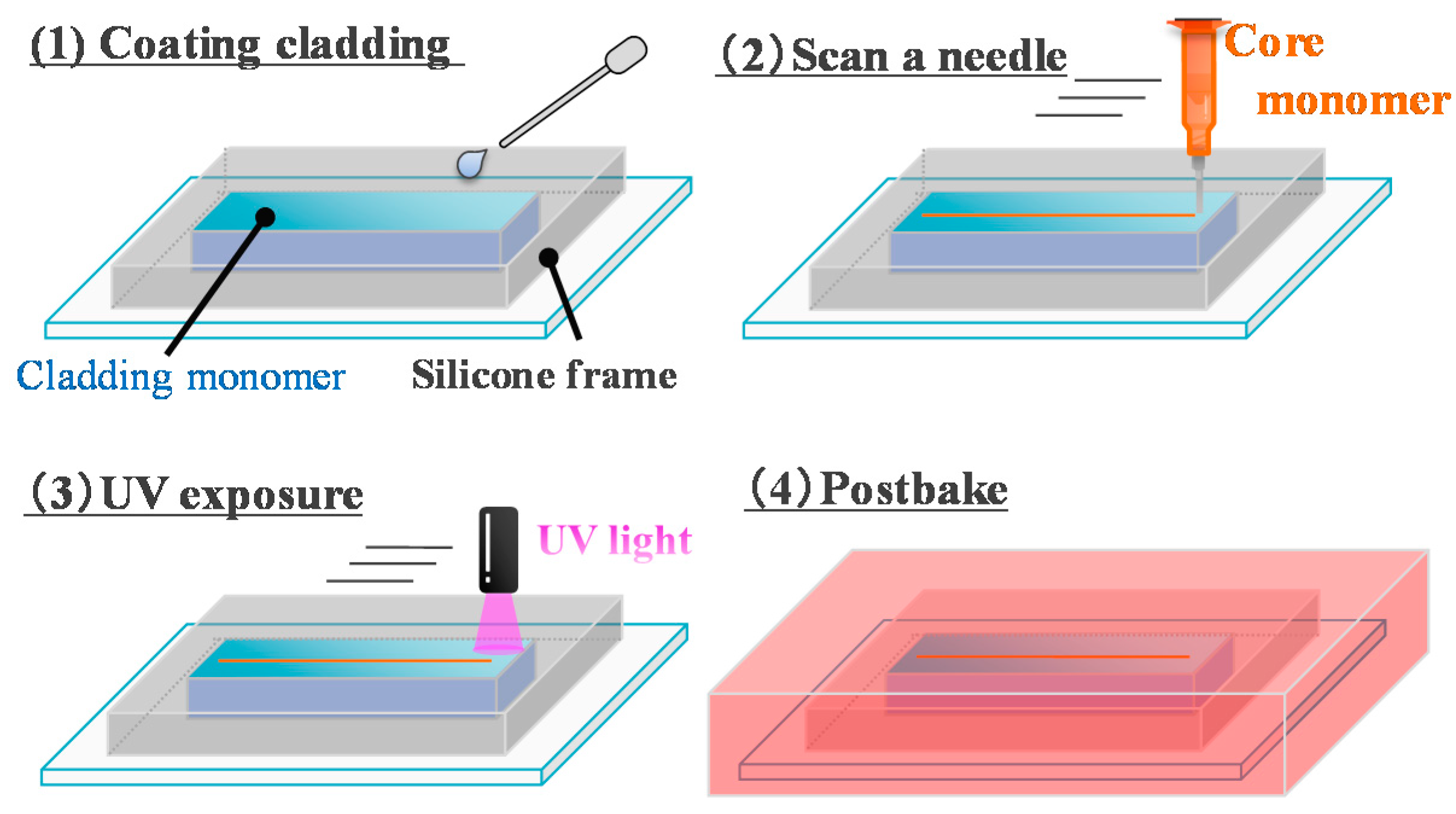
2.1. Mosquito Fabrication Method (Keio University)
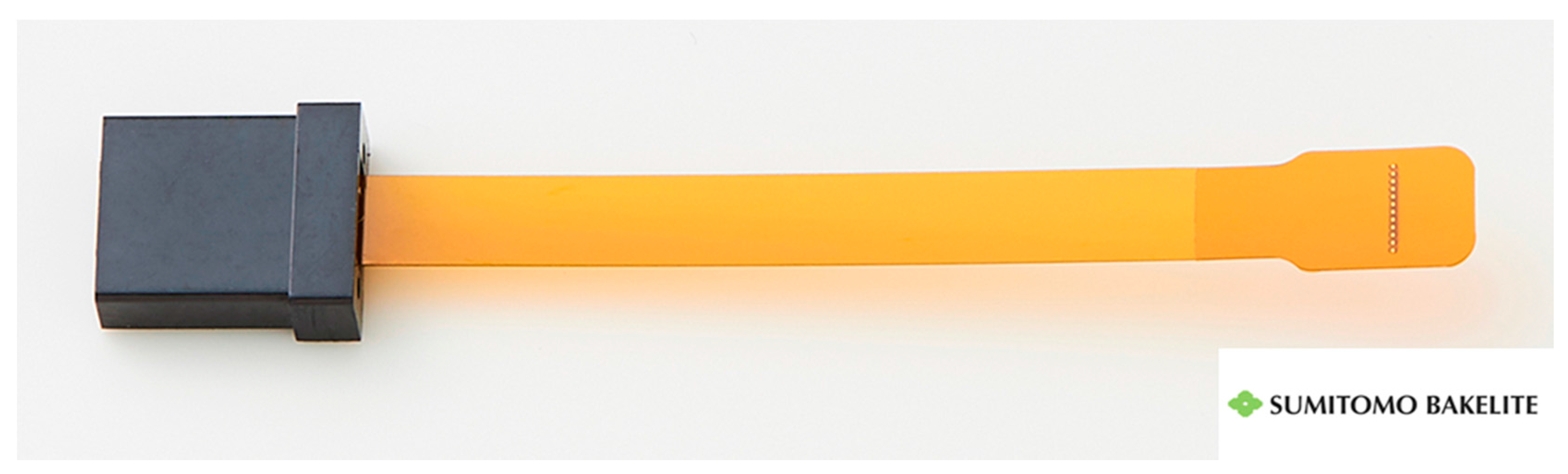
2.2. Photo-Addressing Fabrication Method (Sumitomo Bakelite)
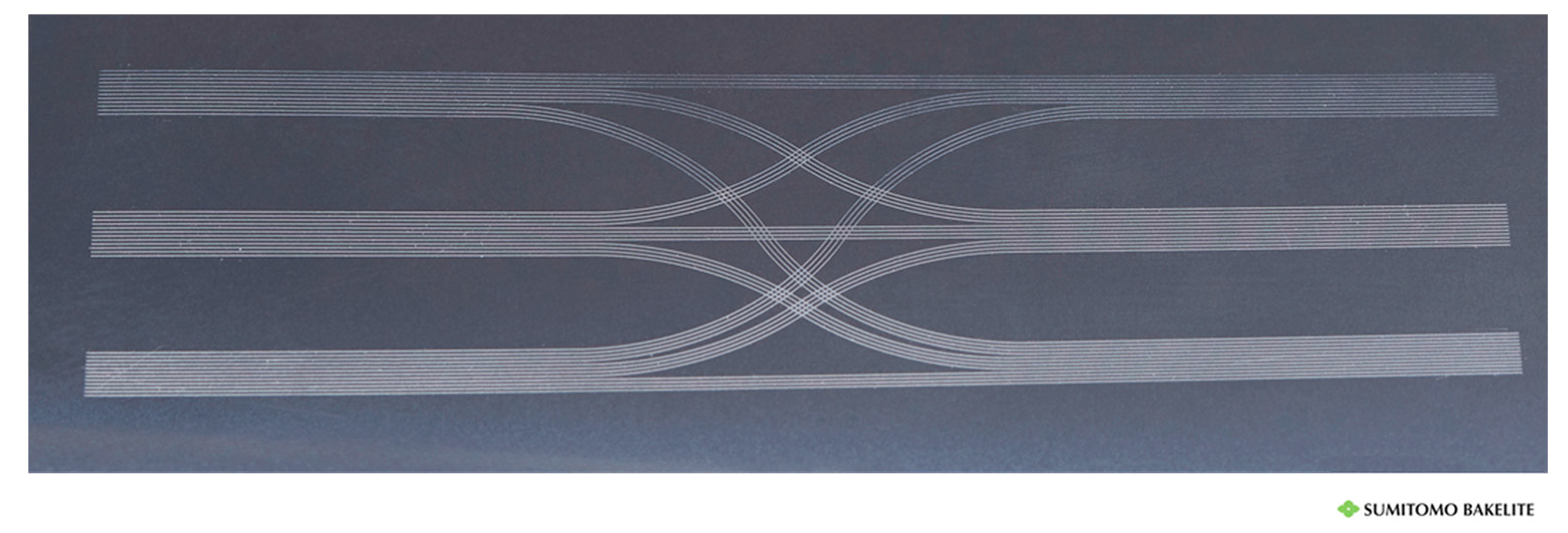
2.3. Waveguide Crossovers
3. Fabrication of Graded Index Glass Waveguides (Fraunhofer IZM)
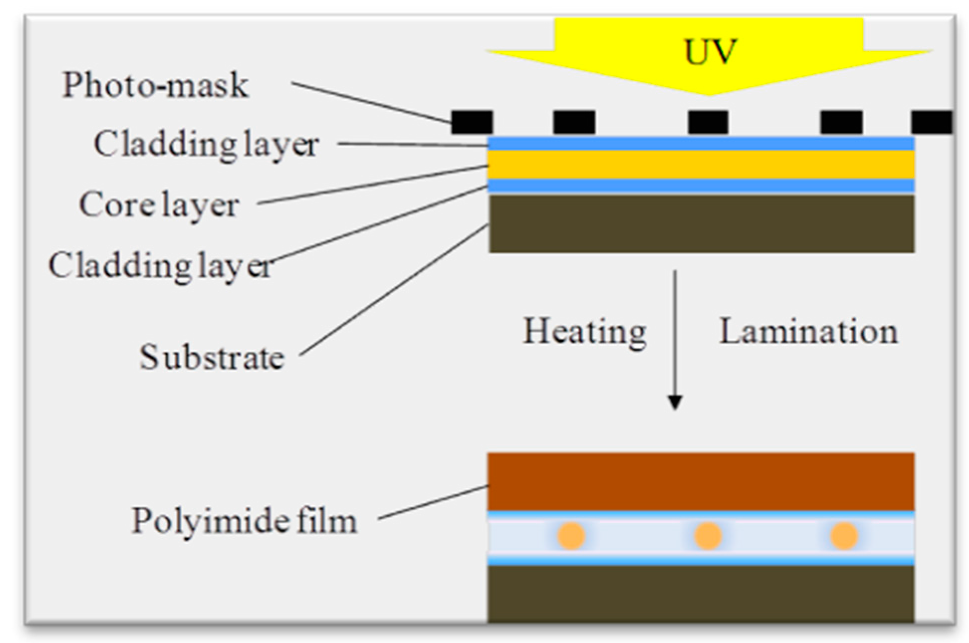
3.1. Two-Step Ion Diffusion Fabrication Process
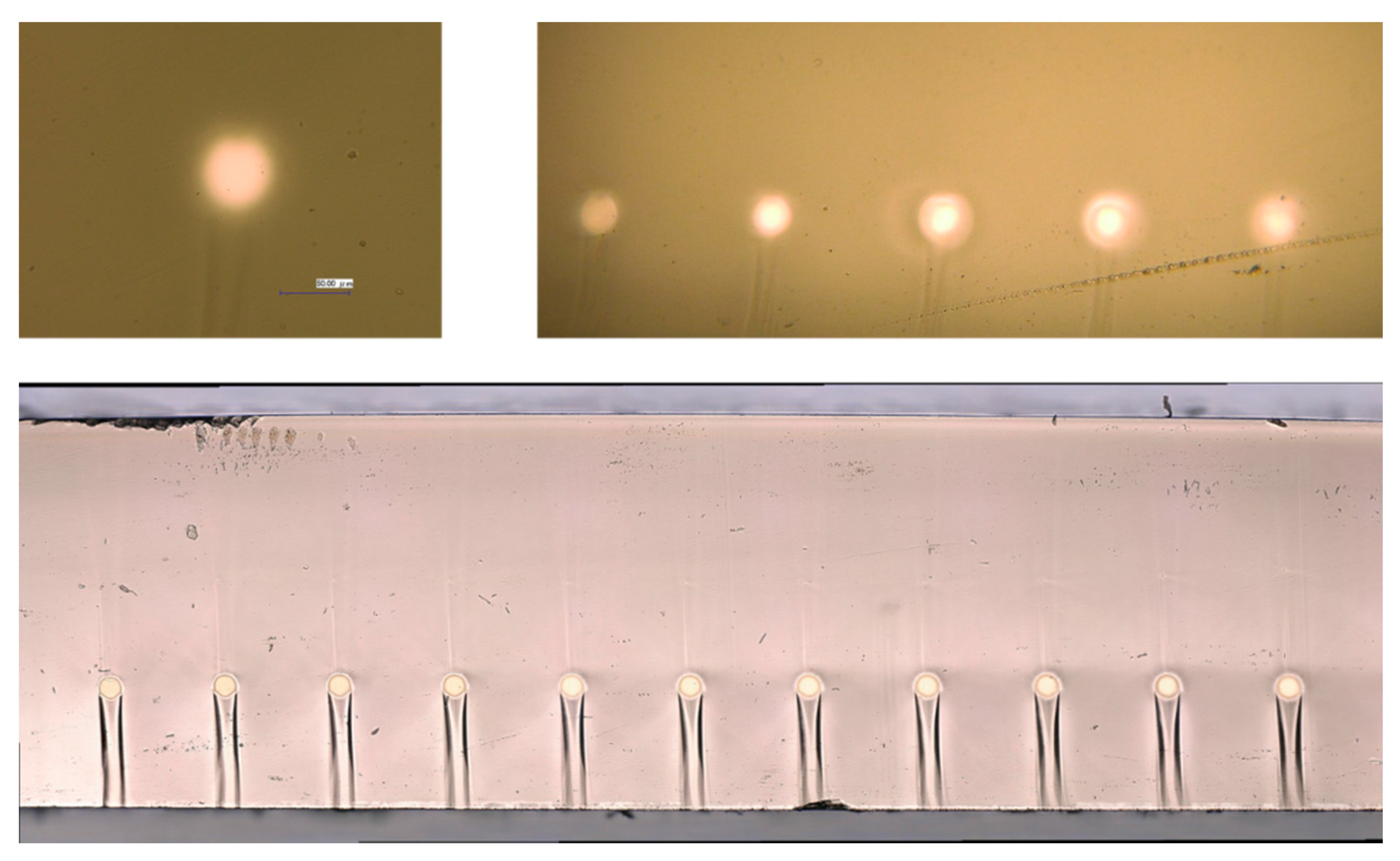
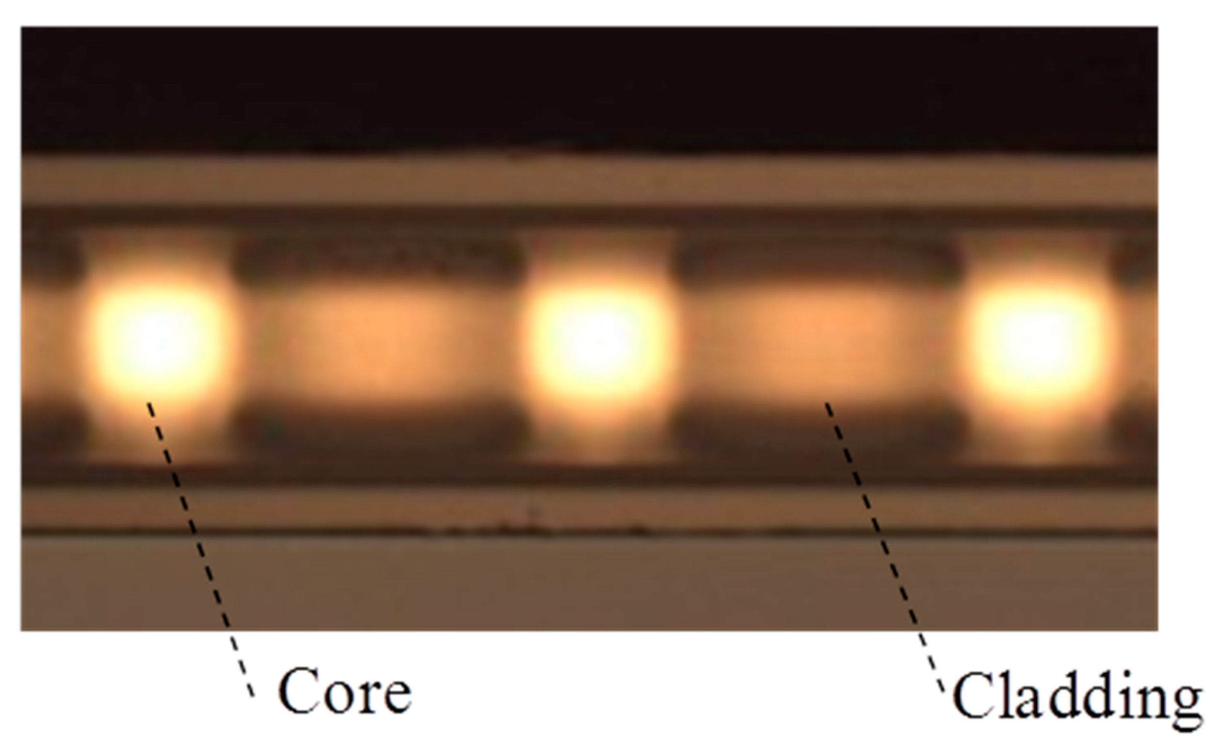
3.2. End Facet Quality Analysis on Glass Waveguides
4. Optical Measurement Process
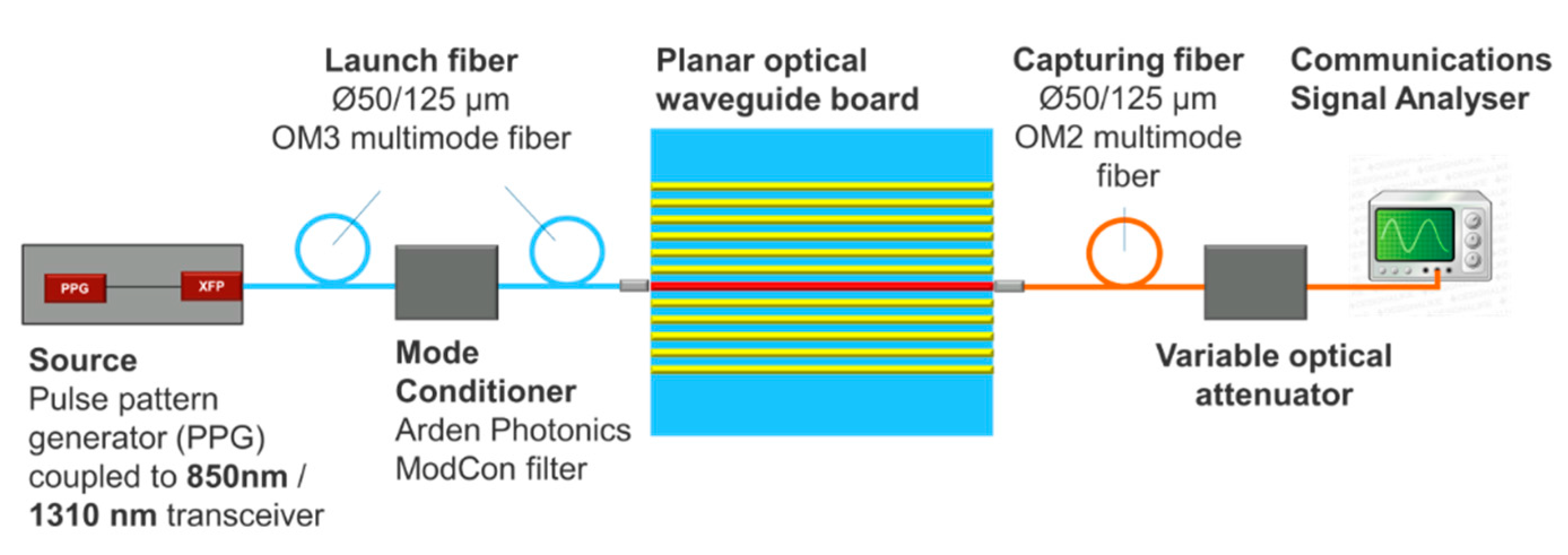
4.1. Optical Waveguide Measurement Set-Up
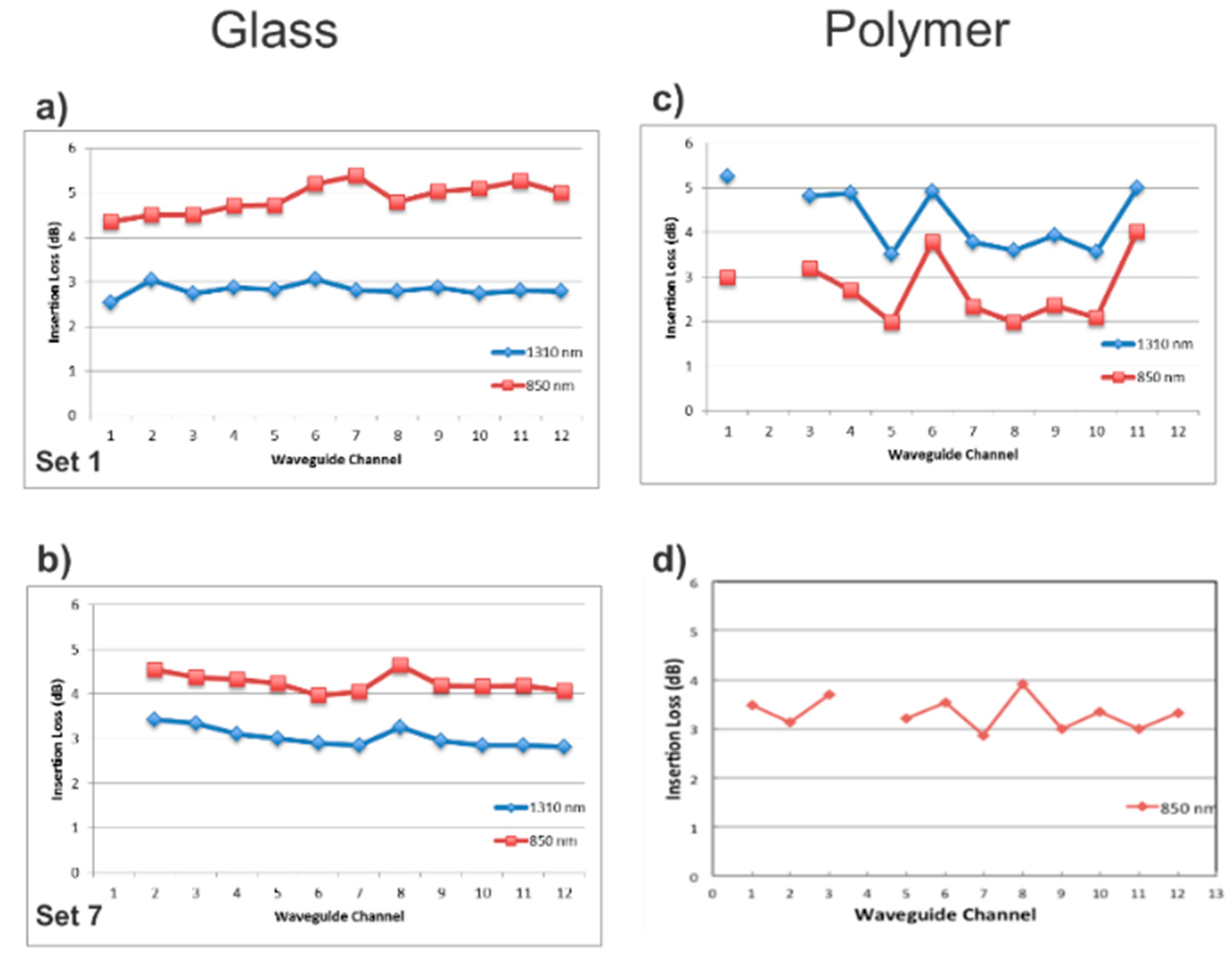
4.2. Comparative Insertion Loss Measurements at 850 nm and 1310 nm
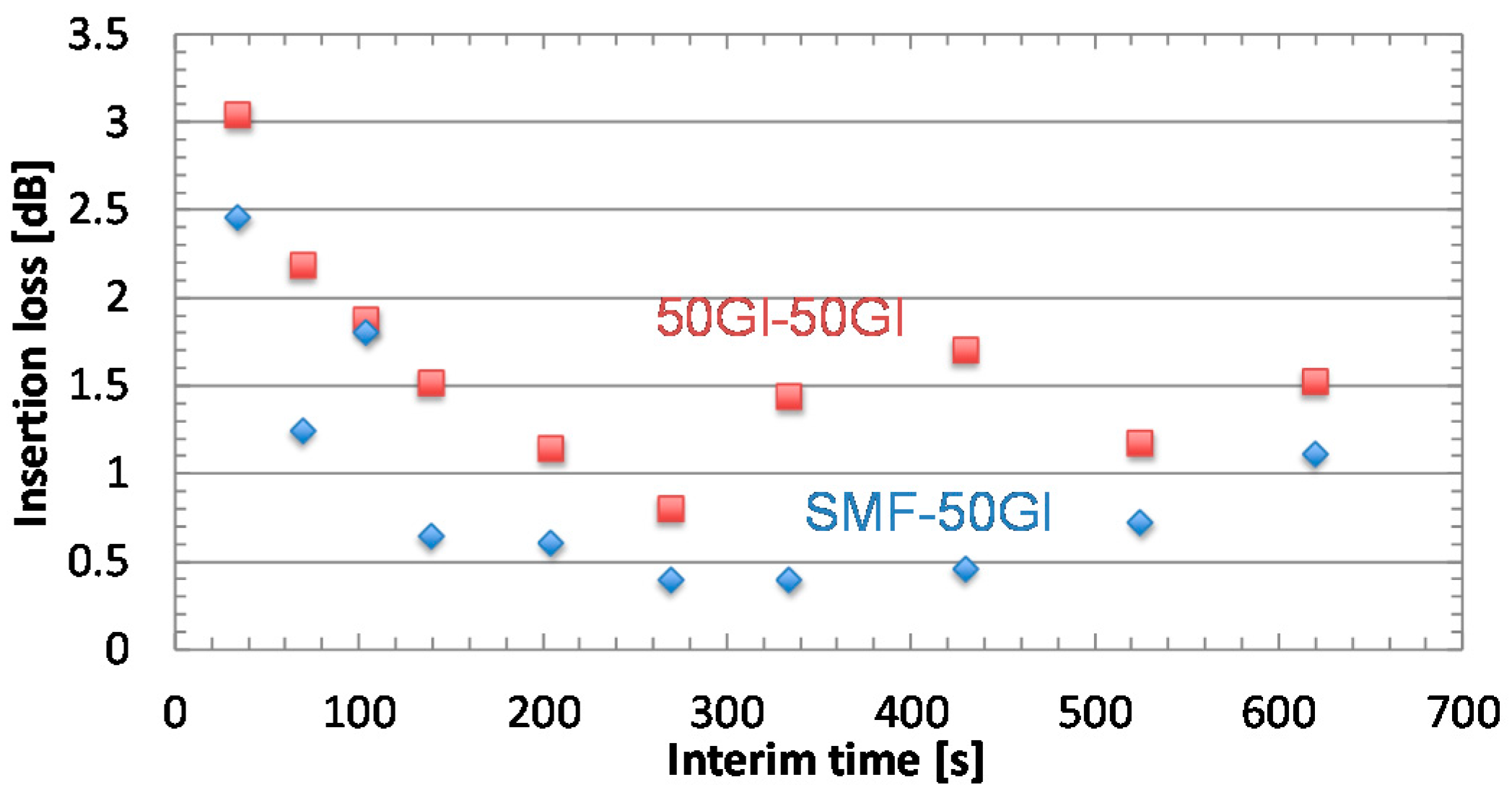
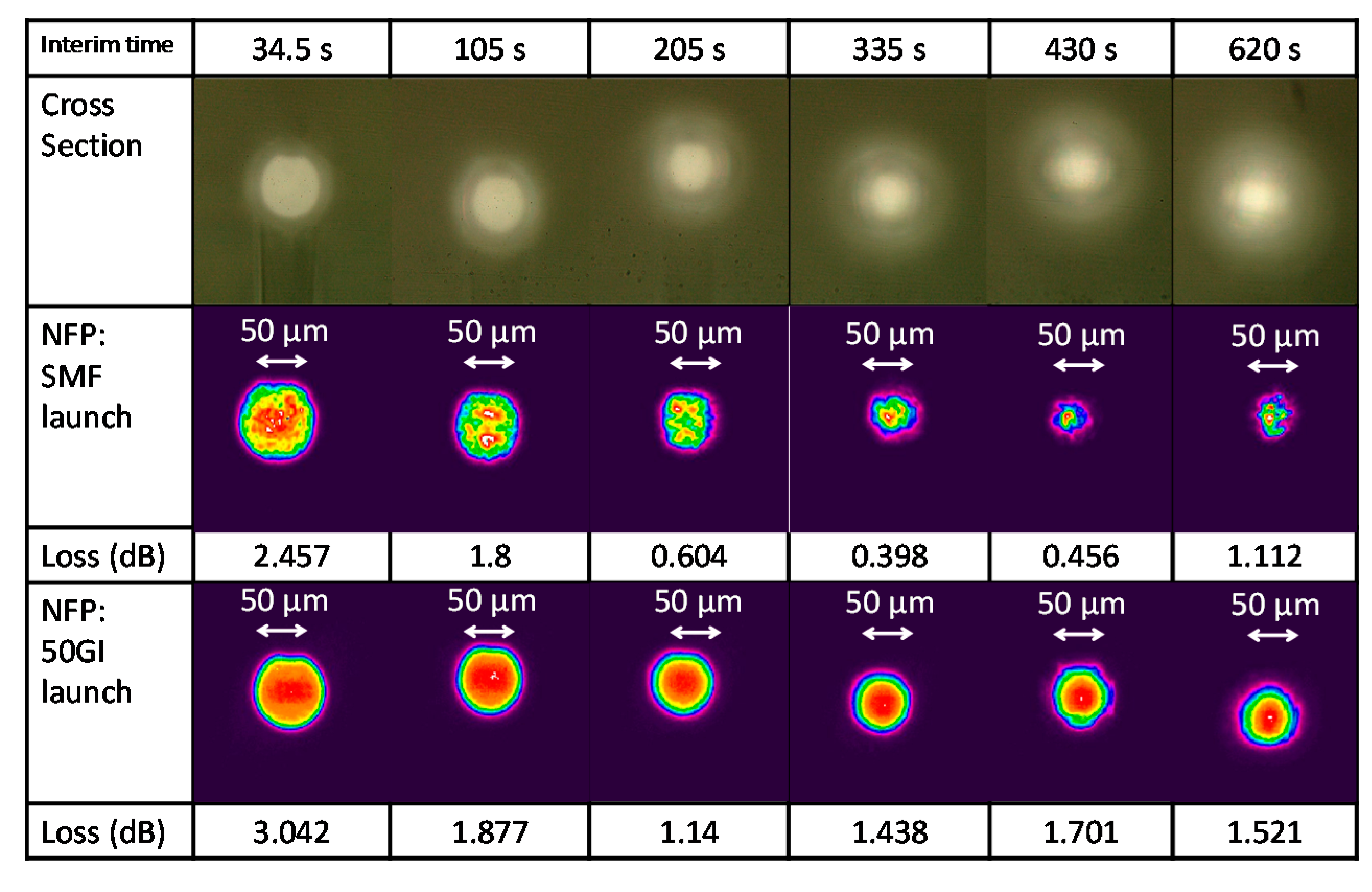
4.3. Loss Analysis of the Waveguides Fabricated Using the Mosquito Method
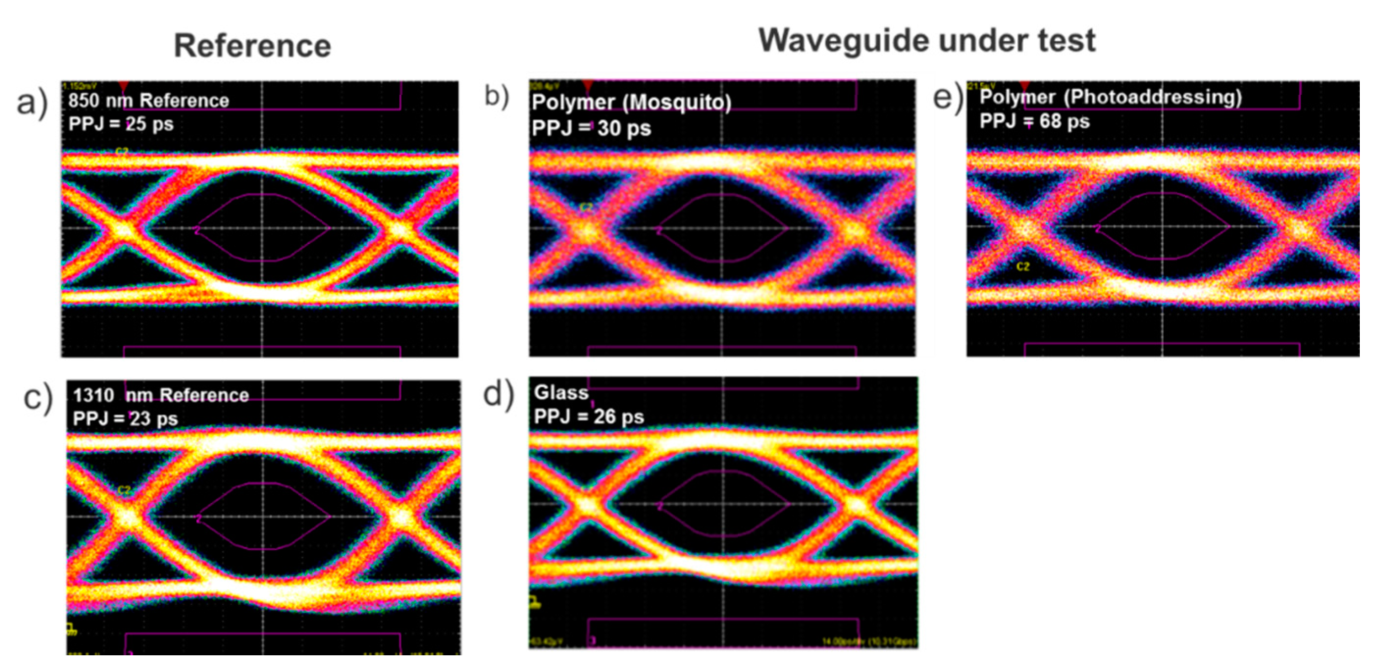
4.4. Signal Integrity Characterization
5. Validation of Different Waveguide Classes in an Optically Enabled Data Center System
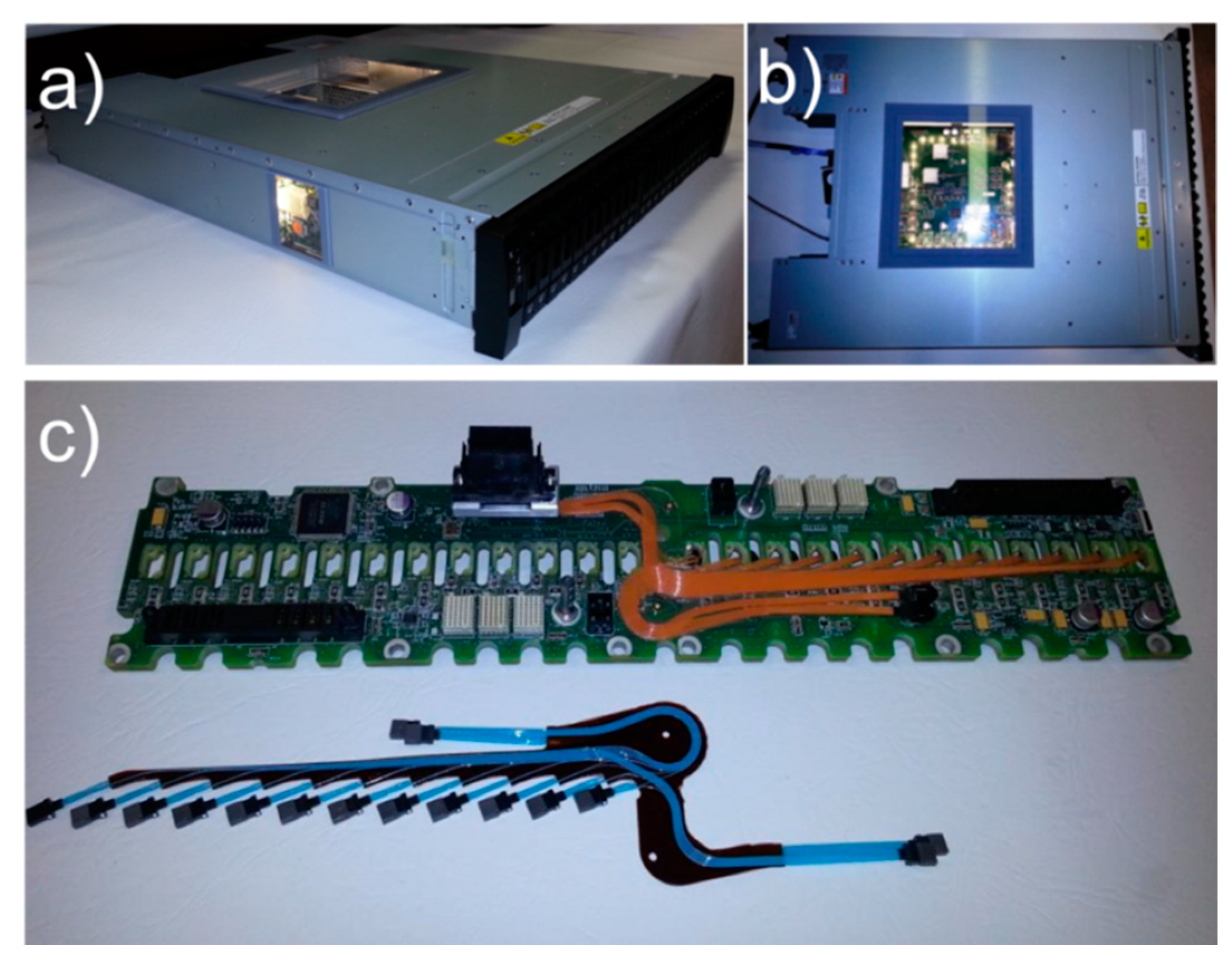
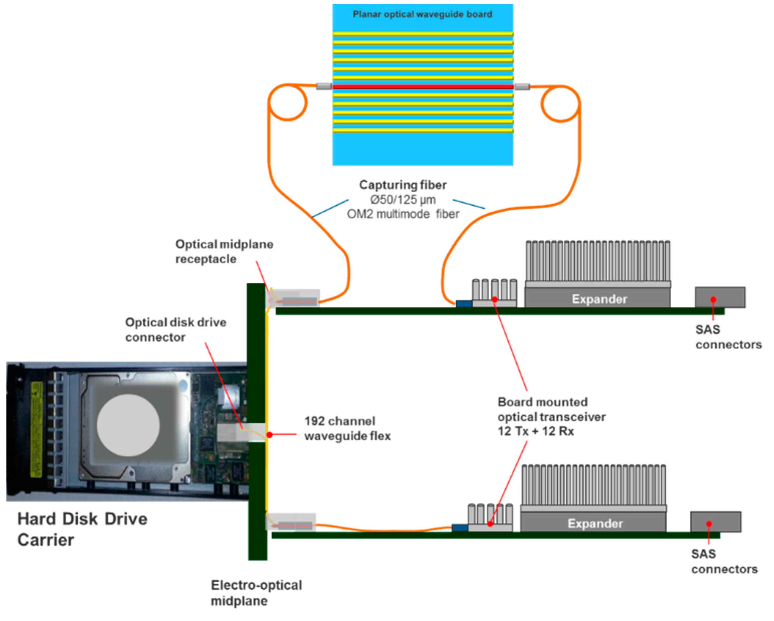
5.1. System Level Measurement Set-Up
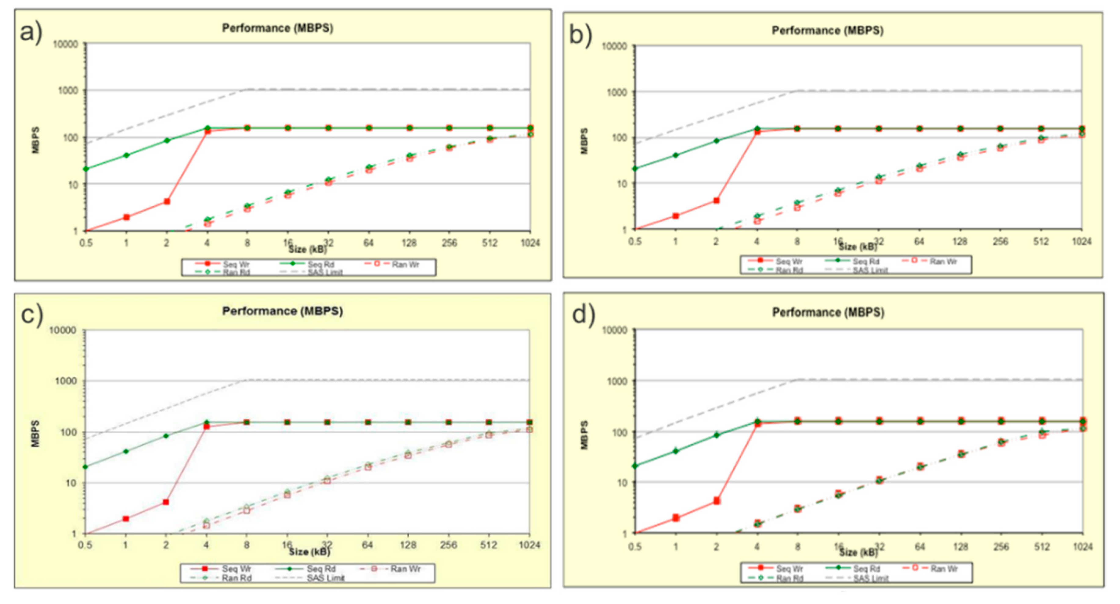
5.2. System Level Measurement Results
6. Conclusions
Acknowledgments
Author Contributions
Conflicts of Interest
References
- Soma, K.; Ishigure, T. Fabrication of a Graded-Index Circular-Core Polymer Parallel Optical Waveguide Using a Microdispenser for a High-Density Optical Printed Circuit Board. IEEE J. Sel. Top. Quantum Electron. 2013, 19, 3600310. [Google Scholar] [CrossRef]
- Ito, Y.; Terada, S.; Singh, M.K.; Arai, S.; Choki, K. Demonstration of High-Bandwidth Data Transmission above 240 Gbps for Optoelectronic Module with Low-Loss and Low-Crosstalk Polynorbornene Waveguides. In Proceedings of the 2012 IEEE 62nd Electronic Components and Technology Conference (ECTC), San Diego, CA, USA, 29 May–1 June 2012; pp. 1526–1531. [Google Scholar]
- Brusberg, L.; Schröder, H.; Herbst, C.; Frey, C.; Fiebig, C.; Zakharian, A.; Kuchinsky, S.; Liu, X.; Fortusini, D.; Evans, A. High Performance Ion-Exchanged Integrated Waveguides in Thin Glass for Board-Level Multimode Optical Interconnects. In Proceedings of the 2015 European Conference on Optical Communication (ECOC), Valencia, Spain, 27 September–1 October 2015. [Google Scholar]
- Pitwon, R.; Brusberg, L.; Schroeder, H.; Whalley, S.; Wang, K.; Miller, A.; Cole, A. Pluggable Electro-Optical Circuit Board Interconnect Based on Embedded Graded-Index Planar Glass Waveguides. J. Light Technol. 2015, 33, 741–754. [Google Scholar] [CrossRef]
- Pitwon, R.; Yamauchi, A.; Brusberg, L.; Wang, K.; Ishigure, T.; Schröder, H.; Neitz, M.; Worrall, A. Planar Polymer and Glass Graded Index Waveguides for Data Center Applications. Opt. Interconnects XIV 2016, 9753. [Google Scholar] [CrossRef]
- Ishigure, T. Graded-index core polymer optical waveguide for high-bandwidth-density optical printed circuit boards: Fabrication and characterization. Opt. Interconnects XIV 2014, 8991, 899102–899110. [Google Scholar] [CrossRef]
- Adeka Corporation. Available online: https://www.adk.co.jp/en (accessed on 1 August 2017).
- Ishigure, T.; Yoshida, S.; Yasuhara, K.; Suganuma, D. Low-loss single-mode polymer optical waveguide at 1550-nm wavelength compatible with silicon photonics. In Proceedings of the 2015 IEEE 65th Electron Components Technology Conference, San Diego, CA, USA, 26–29 May 2015; pp. 768–774. [Google Scholar]
- Horimoto, A.; Kitazoe, K.; Kinoshita, R. Simple channel reconnection using polynorbornene based GI waveguide for optical interconnect. In Proceedings of the 2015 IEEE CPMT Symposium Japan (ICSJ), Kyoto, Japan, 9–11 November 2015; pp. 122–125. [Google Scholar]
- Karabchevsky, A.; Kavokin, A.V. Giant absorption of light by molecular vibrations on a chip. Sci. Rep. 2016, 6, 21201. [Google Scholar] [CrossRef] [PubMed]
- International Electro-Technical Commission. IEC 62496-2:2017 Optical Circuit Boards—Basic Test and Measurement Procedures—Part 2: General Guidance for Definition of Measurement Conditions for Optical Characteristics of Optical Circuit Boards. 2017. Available online: https://webstore.iec.ch/publication/32157 (accessed on 1 June 2017).
- International Electro-technical Commission. IEC 61280-4-1:2009 Fibre-Optic Communication Subsystem Test Procedures—Part 4-1: Installed Cable Plant—Multimode Attenuation Measurement; International Electro-Technical Commission: Geneva, Switzerland, 2009. [Google Scholar]
- Watanabe, T.; Ooba, N.; Hayashida, S.; Kurihara, T.; Imamura, S. Polymeric Optical Waveguide Circuits Formed Using Silicone Resin. J. Light Technol. 1998, 16, 1049. [Google Scholar] [CrossRef]
- Pitwon, R.; Worrall, A.; Stevens, P.; Miller, A.; Wang, K.; Schmidtke, K. Demonstration of fully enabled data center subsystem with embedded optical interconnect. Opt. Interconnects XIV 2014, 8991, 899110. [Google Scholar] [CrossRef]
- Intel Corporation. Iometer Project. Available online: http://www.iometer.org/ (accessed on 11 January 2016).


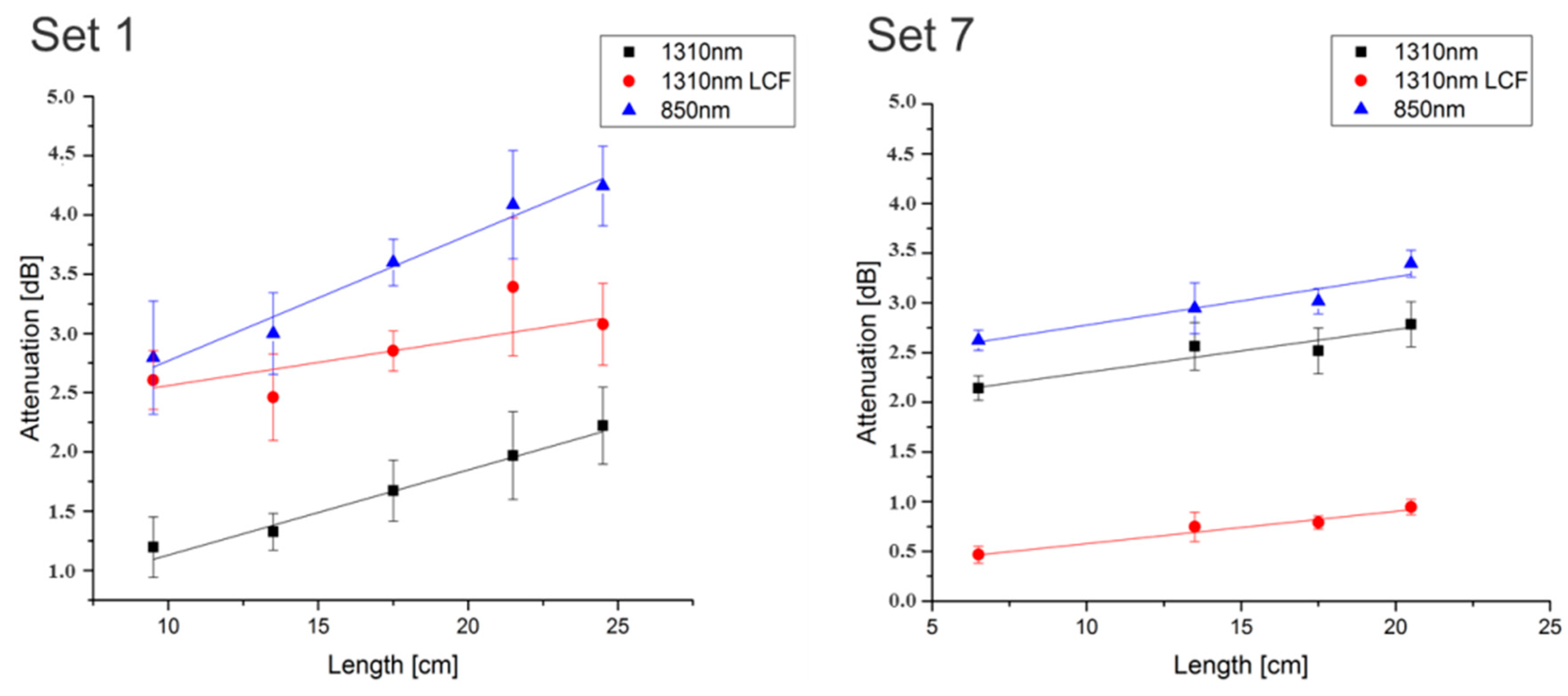
| Wavelength | Set 1 | Set 7 | ||
|---|---|---|---|---|
| GI 50 launch fiber | PL (dB/cm) | IL (dB) | PL (dB/cm) | IL (dB) |
| 850 nm | 0.11 ± 0.01 | 1.71 ± 0.19 | 0.05 ± 0.01 | 2.29 ± 0.14 |
| 1310 nm | 0.07 ± 0.008 | 0.41 ± 0.12 | 0.04 ± 0.008 | 0.25 ± 0.1 |
| Large Core Fiber | Set 1 | Set 7 | ||
| 850 nm | 0.04 ± 0.014 | 2.17 ± 0.24 | 0.03 ± 0.004 | 1.87 ± 0.06 |
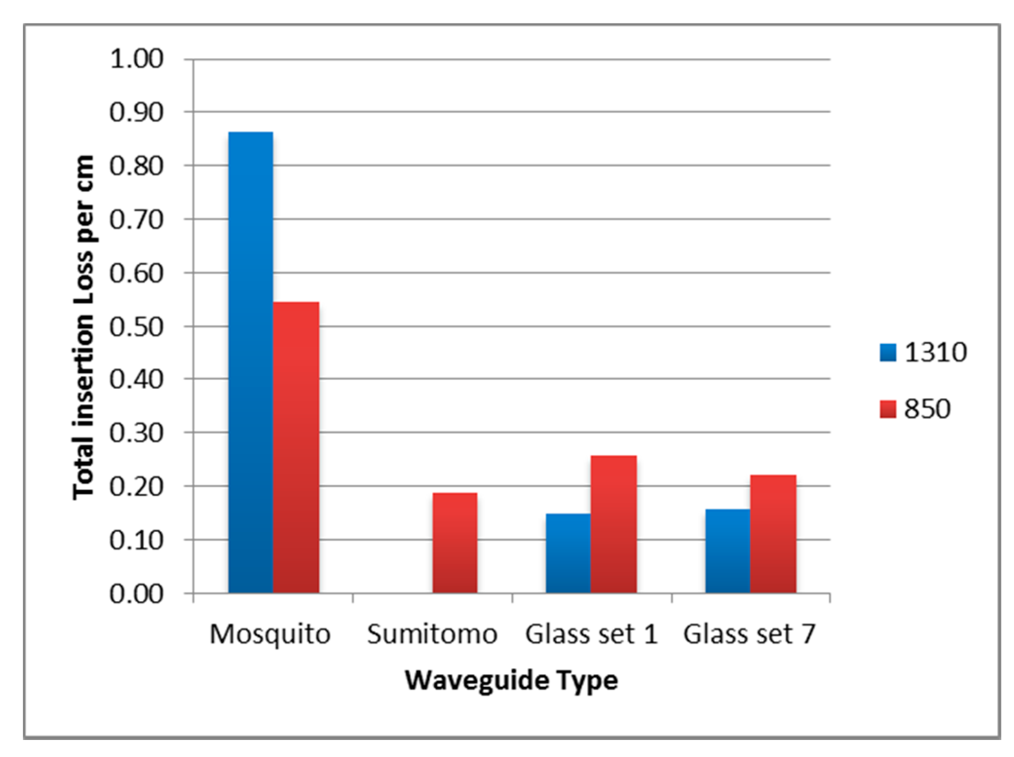
| Parameters | Mosquito Waveguides | Sumitomo Waveguides | Glass Waveguides | |
|---|---|---|---|---|
| Set 1 | Set 7 | |||
| Core, n1 | (NP-005), 1.597 | - | 1.523 | 1.527 |
| Cladding, n2 | (NP-208), 1.569 | - | 1.498 | 1.498 |
| Index difference | 0.028 | 0.025 | 0.029 | |
| Sample length | 5 cm | 17.6 cm | 19 cm | 19 cm |
| Optical layer thickness | 0.5 mm | 0.1 mm | 0.55 mm | 0.55 mm |
| Core size | ~50 μm | ~50 μm | ~50 μm | ~50 μm |
| Channel Pitch | 250 μm | 250 μm | 250 μm | 250 μm |
| Fab. method | Mosquito | Photo addressing | Ion diffusion | Ion diffusion |
| Index Profile | GI | GI | Elliptical GI | Elliptical GI |
| Input Wavelength (nm) | Insertion Loss (dB) | |||
|---|---|---|---|---|
| Mosquito Waveguide | Photo-addressed Waveguide | Glass Waveguide | ||
| Set 1 | Set 7 | |||
| 850 | 2.73 ± 0.69 | 3.32 ± 0.31 | 4.90 ± 0.32 | 4.23 ± 0.20 |
| 1310 | 4.32 ± 0.67 | Not available | 2.81 ± 0.13 | 3.00 ± 0.21 |
© 2017 by the authors. Licensee MDPI, Basel, Switzerland. This article is an open access article distributed under the terms and conditions of the Creative Commons Attribution (CC BY) license (http://creativecommons.org/licenses/by/4.0/).
Share and Cite
Pitwon, R.; Wang, K.; Yamauchi, A.; Ishigure, T.; Schröder, H.; Neitz, M.; Singh, M. Competitive Evaluation of Planar Embedded Glass and Polymer Waveguides in Data Center Environments. Appl. Sci. 2017, 7, 940. https://0-doi-org.brum.beds.ac.uk/10.3390/app7090940
Pitwon R, Wang K, Yamauchi A, Ishigure T, Schröder H, Neitz M, Singh M. Competitive Evaluation of Planar Embedded Glass and Polymer Waveguides in Data Center Environments. Applied Sciences. 2017; 7(9):940. https://0-doi-org.brum.beds.ac.uk/10.3390/app7090940
Chicago/Turabian StylePitwon, Richard, Kai Wang, Akira Yamauchi, Takaaki Ishigure, Henning Schröder, Marcel Neitz, and Mayank Singh. 2017. "Competitive Evaluation of Planar Embedded Glass and Polymer Waveguides in Data Center Environments" Applied Sciences 7, no. 9: 940. https://0-doi-org.brum.beds.ac.uk/10.3390/app7090940