A Distribution Power Electronic Transformer with MMC


1
Department of Electrical Eng. and IT, DIETI, University of Naples Federico II, 80125 Naples, Italy
2
GETRA Engineering & Consulting, 81025 Caserta, Italy
*
Author to whom correspondence should be addressed.
Appl. Sci. 2018, 8(1), 120; https://0-doi-org.brum.beds.ac.uk/10.3390/app8010120
Submission received: 4 December 2017
/
Revised: 28 December 2017
/
Accepted: 12 January 2018
/
Published: 16 January 2018
Abstract
:This paper deals with a Power Electronic Transformer (PET) topology for a 3-phase AC distribution grid. In the discussed topology, a Modular Multilevel Converter (MMC) and a Full-Bridge converter are employed for the medium voltage (MV) and the low voltage (LV) side, respectively. By using the space vector, approach a mathematical model for the MMC is presented and a grid-synchronous algorithm is implemented to easily control the power flow through the structure. The MV and LV side converters are linked through a High Frequency (HF) transformer, whose control strategy is a Dual-Active Phase-Shift Control (PSC) with Square Wave Modulation (SQM). This technique is combined with a predictive algorithm, which is able to keep each leg’s capacitors’ voltages balanced both in stationary and in transient conditions. The proposed algorithm is numerically validated in the Matlab/Simulink® environment.
1. Introduction
The global energy market, strictly dependent on fossil fuels, requires substantial changes in order to target more environmentally sustainable energy sources. Indeed, the increase of renewable energy sources (RESs), while ensuring a significant reduction in CO2 emissions, requires a deep upgrade of the transmission and/or distribution network in order to capitalize the contribution of complex interconnected systems [1,2]. This implies the adoption of an advanced electric system, which, by employing innovative technologies, ensures smart management of both energy and power flows. Indeed, the typically intermittent and non-programmable nature of RESs, needs a substantial modification of the electric grid, which must adapt to the locations and times of availability of such sources; therefore, it must ensure the energy supply required by users, operating with a novel management/control approach; in this context, the end user becomes a “prosumer”, i.e., a producer and not just a consumer.
This evolution process has started an infrastructure upgrade of the power grids, with the increase of system interconnections, the creation of new nodes (stations), and the development of real-time management systems. This revolution can be achieved only after an overall upgrade of the system components.
Power Electronic Transformers (PETs) have been identified as emerging clever electronic devices in the future smart grid [3,4,5], especially for applications of renewable energy conversion and management [6,7]. Considering that the PET is directly connected to a medium-voltage grid, e.g., a 20 kV distribution system, its structural issues are more complex and severe. Different topologies have been presented and discussed in the literature relating to a realization in distribution grid applications [8,9,10,11]. The most consolidated topology performs either voltage transformation or power quality management, using power electronics both on primary and secondary side of a transformer that operates in medium frequency [12,13,14,15]. Therefore, a frequency converter on each side of the transformer is needed. The requirements of reliability, availability, safety, and maintenance suggest the use of multilevel architectures in order to exploit their intrinsic advantages in terms of voltage withstand properties and to improve robustness to the faults in power electronics converters. Therefore, the proposed architecture for a 3-phase MV AC distribution grid is built around a Modular Multilevel Converter, based on several low-voltage cells, each one being a Full-Bridge converter with a dedicated DC-Link capacitor.
The LV distribution grid is fed through a three-phase/four-wires Voltage Source Inverter (VSI), whereas the galvanic insulation is achieved thanks to a central single-phase transformer, which operates at high frequencies.
This paper proposes a new modulation technique, with the aim to ensure the balancing between each submodules of the same leg of the MMC [16]. Indeed, thanks to an optimized sorting algorithm, which acts upon the compensated current leg based on a predictive correction, the capacitors voltages are kept balanced both in stationary and transient conditions.
2. System Topology
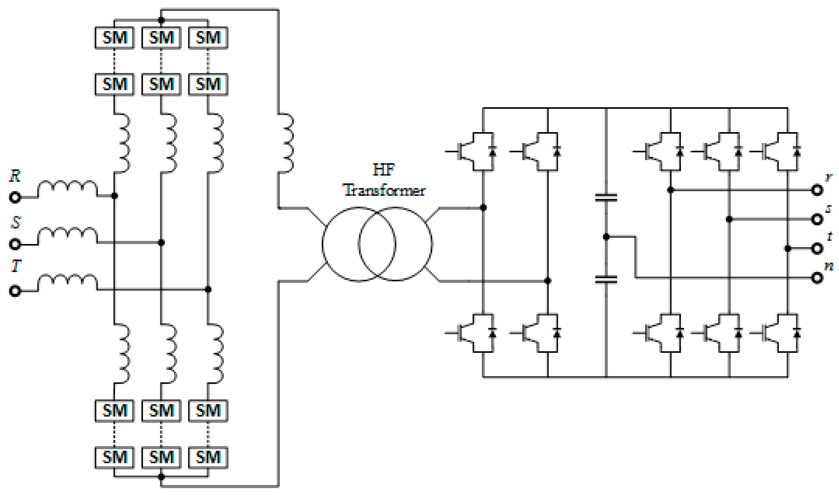
The Power Electronic Transformer under analysis interconnects a three-phase 50 Hz/20 kV MV grid with a three-phase 50 Hz/400 V LV grid. The rated power of the considered system is 100 kVA. As shown in Figure 1, the proposed topology consists of three main blocks:
- MV-side power converter, which transforms the LF AC voltage of the MV grid into a single-phase HF AC square-wave voltage;
- LV-side power converter, which transforms the LF AC voltage of the LV grid into a single-phase HF AC square-wave voltage;
- HF transformer, which links and guarantees galvanic insulation between the MV-side and the LV-side power converters.
A Full Bridge–based MMC is used on the system MV-side in order to exploit its intrinsic ability to sustain high voltages with a simple increment of the number of submodules.
The chosen LV-side converter is instead a two-stage system: one stage is a Full-Bridge Inverter (on the HF-side), while the second stage is a three-phase/four-wires VSI (on the load side).
3. Mathematical Model
The mathematical model of the system can be written with some simplifying hypotheses. In particular, under the assumption that the capacitor of each submodule doesn’t suffer large voltage perturbations during a single switching period and by neglecting the rise/fall time of the IGBTs, each leg of the converter can be represented as an ideal controllable voltage source, whose output depends on the instantaneous voltages of its submodules capacitors and on the switching signals applied to the submodules IGBTs. Moreover, it is reasonable to neglect the effect of the inductors’ resistances and the difference between their inductances.
The KVLs applied through each leg give
where is the k-th grid phase voltage, is the k-th grid current, and are the k-th currents (flowing through the top and the bottom MMC converter legs, respectively), and and are the voltages measured between the ideal ground G and the transformer side output terminals T and B. In particular, as it can be seen in Figure 2, while the grid voltages are the input of the MMC converter, the voltage is the controllable output that actually feeds the primary side of the HF transformer.
A simple equation for the transformer MV-side current can be found once the transformer magnetizing current is neglected [17].
where is the transformer’s LV-side voltage referred to the MV-side and is the sum of the leakage inductances and of optional additional external series inductances. Naturally, can be obtained as
By using the space vector and zero sequence components, defined as
and by introducing the average and differential quantities, defined as
the system model can be rewritten as
where is the grid-side equivalent inductance, while is the transformer-side equivalent inductance.
From the proposed model, it is evident how it is necessary to guarantee a balancing of the voltages on the capacitors of all the modules in order to appropriately control the power flows through the PET. Indeed, Equation (6) can be easily exploited with respect to the definition of the control strategy only if the capacitor voltages are assumed quasi-constant; in this case, each module can be modeled with a voltage generator driven by a constant source. In [18] the authors proposed an analytically based steady state model of the MMC in order to highlight the dependencies of the modules DC sides voltages behavior from the system operating condition and filter parameters. However, the proposed method refers to an MMC driven by a DC source for high-voltage DC (HDVC) systems, for which the DC sides of the converter are forced by unbalancing powers characterized by two predominant harmonics at (dependent only on the AC currents) and (dependent on the AC currents and on the modulation index), with the AC output frequency. In the case of an MMC used as a high voltage stage in PET configurations, only the harmonic at can be considered, since the transformer side voltage generates an unbalancing power oscillating at the transformer frequency, whose effect can be neglected. Moreover, the converter works with quasi-constant modulation index. In this context, if the capacitors are sized in order to contain the ripple at within a sufficiently low desired value, second order effects can be assumed negligible. Therefore, a capacitors balancing algorithm can be easily formulated with the aim to ensure a stable operation in all operating conditions (i.e., transient and/or steady state), since the uneven power absorption across the converter modules during the modulation interval requires a re-balancing of the capacitors stored energy. The capacitors balancing can be achieved by controlling the recirculating current, as shown in the following section. The LV-side three-phase/four-wires VSI is independent from the transformer stage and, therefore, can be easily modeled as a power-controlled ideal current source.
4. Control Strategy
According to the first relation of Equation (1), the space vector of the grid currents can be controlled through the MMC space vector voltage ; its reference can be computed in order to achieve a proper control of the active/reactive power flow from the MV grid to the PET. Indeed, the instantaneous values of the grid powers can be evaluated as
By expressing the space vector of the grid voltages as and by referring the space vector of the grid currents to the reference frame identified by the angle , Equation (7) can be rewritten as
where the direct/quadrature components are defined by the position Equation (8) highlights the linear dependence between the grid powers and the related currents space vector components. Therefore, the control of can be performed by a proper tracking of , which can be effectively performed by means of simple PI regulators.
While the instantaneous voltage phase and magnitude can be obtained through a dq-based three-phase PLL [19], the active power flow through the grid can be driven by a voltage controller used in order to keep constant the total energy stored in the MMC capacitors. The reference value of the reactive power is instead set to zero with the aim to maximize the system energetic efficiency, reducing the grid-side currents’ RMS.
The second relation of Equation (6) defines the dynamical behavior of the space vector of the differential currents, which represents recirculating currents for the MMC. It should be ideally set to zero in order to minimize the RMS values of the MMC currents, but can be used for balancing purposes, i.e., phase to phase balancing and upper to lower balancing.
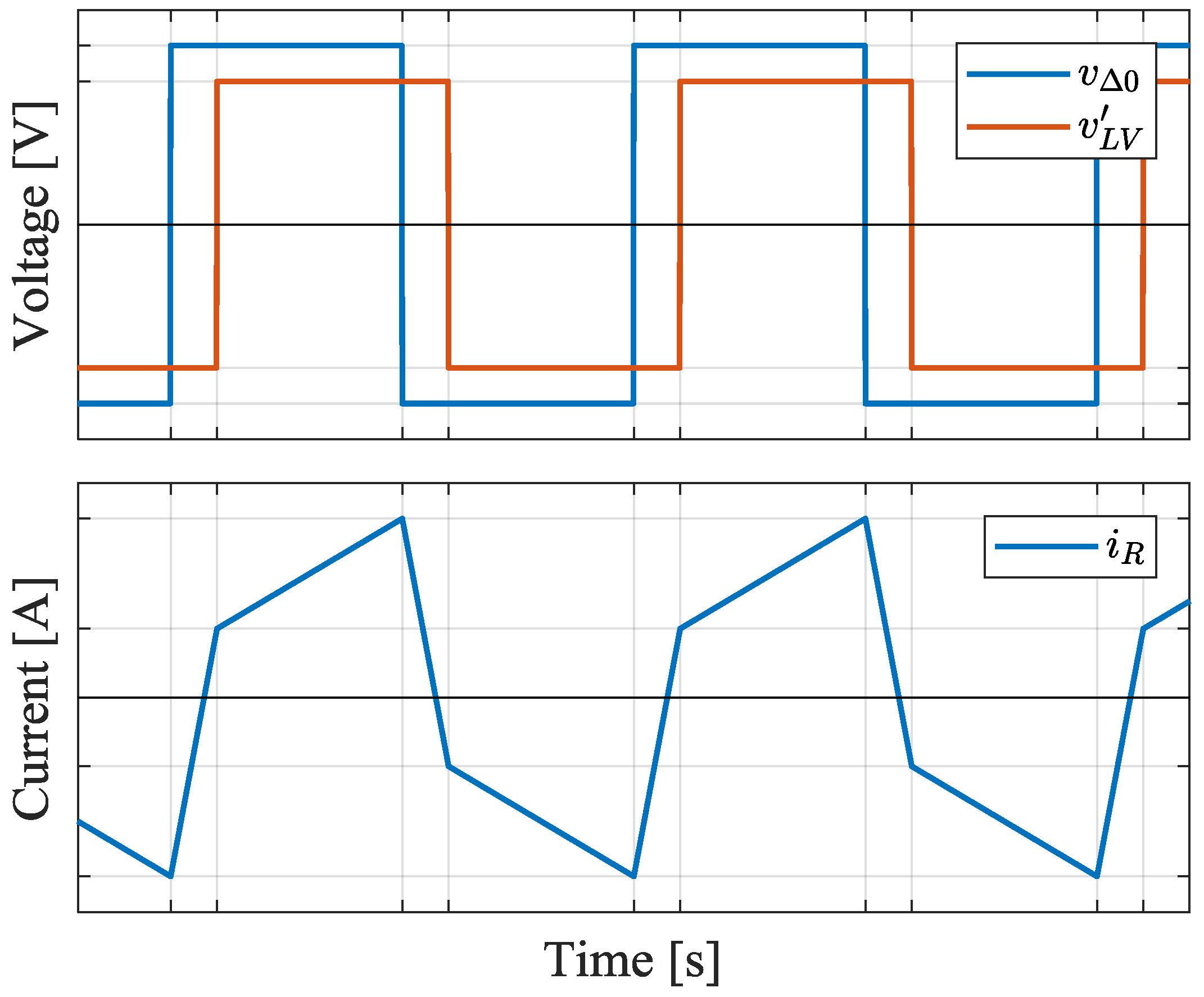
The last relation of the Equation (6) defines, instead, the dynamical behavior of the MF transformer primary side current , which depends on the voltage difference . The transformer power flow is controlled by means of a PSC algorithm with Square Wave Modulation (SQM): both the MMC voltage and the LV-side Full Bridge Inverter voltage are forced as square waves with the same frequency and with magnitude respectively and ; the control of the power flow computes the time shift delay of the Full-Bridge square wave with respect to the MMC square wave, which is chosen as reference in order to simplify the converter modulation implementation.
By neglecting the transformer magnetizing current and the circuit resistances, the current behavior can be assumed piece-wise linear. The ideal waveforms of the primary/secondary voltages and of the primary current are depicted in Figure 3.
In steady state conditions the power flow through the MF transformer is linked to the applied time shift through the well-known relation [17]
while the maximum achievable power can be expressed as
The reference value of the transformer current in correspondence of the switching instants can be obtained through the steady state relation
while a predictive algorithm is used to compute the time delay which ensures the desired condition ; the following relation is easily obtained:
where is the measured value of the transformer current.
Finally, the PSC reference power is obtained as the output of a voltage controller aimed to stabilize the LV-side converter DC-Link around its nominal value . A simple PI controller is suitable for this purpose. This value can be chosen in order to achieve the optimal condition , which guarantees that the transformer current , in steady state conditions, is a trapezoidal wave with magnitude .
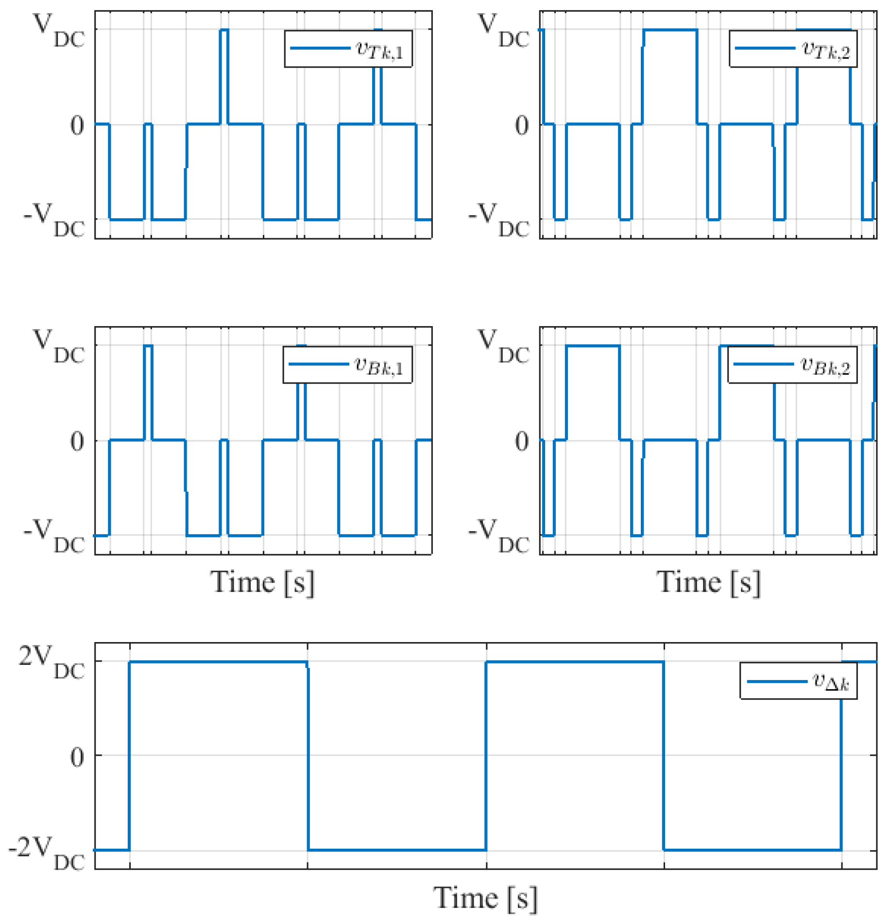
While the LV-side Full-Bridge AC output voltage depends only on its DC-Link voltage, which is kept practically constant in a modulation time interval, the MMC MF side output voltage strongly depends on the converter operations. Indeed, an ideal square wave voltage can be generated only if all the converter modules are perfectly balanced and no differential voltage is injected in the modules AC outputs. In this case, an ideal square wave is produced if the top and bottom legs of each converter phase are switched in a complementary way, as exemplified in Figure 4 for the generic phase k of an ideal two modules converter: since the voltage () of the first (second) top module has the same switching instants of the corresponding bottom module’s voltage (), the differential output is perfectly constant for the entire switching period.
A symmetrical switching of the upper and lower converters is automatically obtained if the upper and lower converters are driven by two Space Vector PWMs (SVPWM) forced with the same voltage reference and if the converters modules are treated as positive charged Half Bridge converters in the positive square voltage half period and as negative charged Half Bridge converters in the negative half period. Therefore, the square wave output period is at least twice the sampling time interval. The actual voltage output behavior deviates from the ideal one depicted in Figure 4 as a consequence of modules voltage unbalancing and asymmetrical modulation of the upper and lower converters.
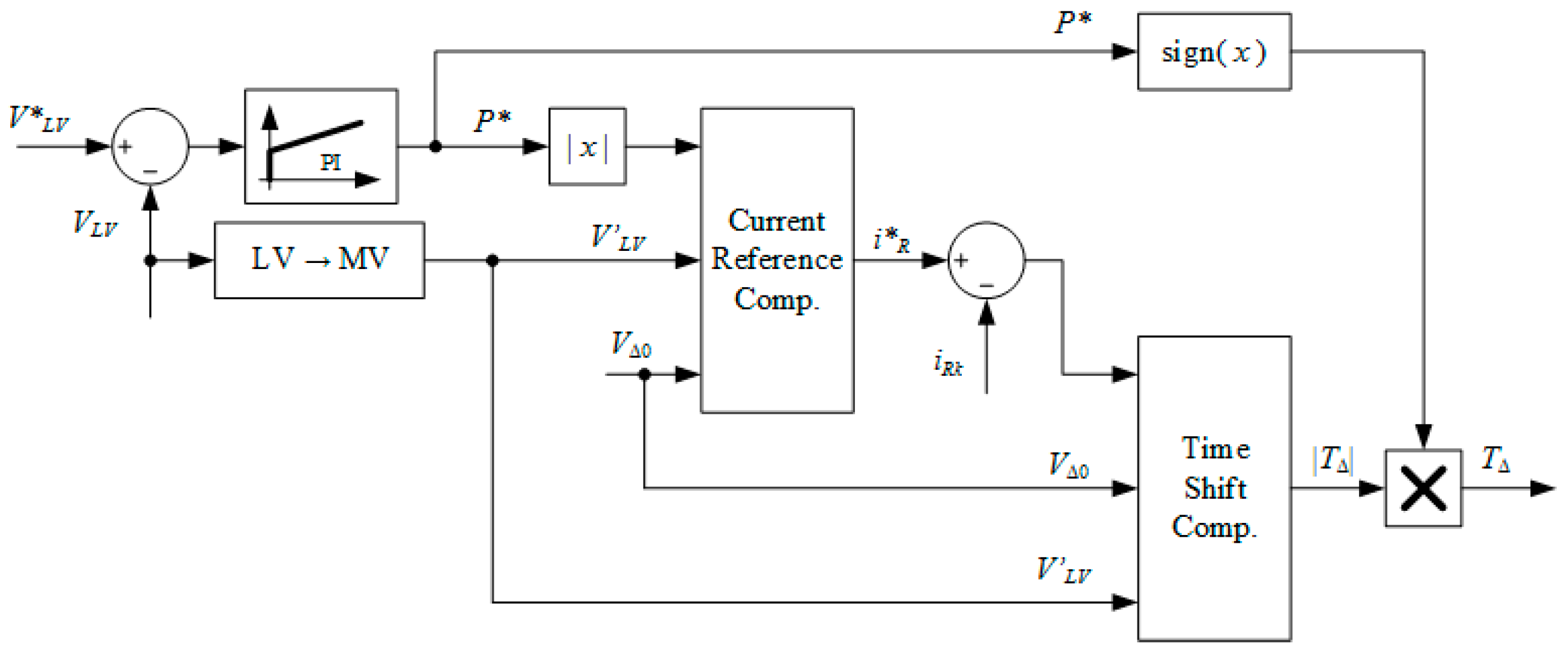
The overall control scheme of the LV-side Full-Bridge converter is shown in Figure 5.
The balancing between the submodules of the same leg can be obtained through a simple sorting algorithm [16,20]. Once the leg reference voltage has been determined through the SVPWM algorithm, the modules are arranged in increasing (decreasing) order of voltage if the leg power is positive (negative): the output voltage is obtained through the switching of the first submodules of the array. The leg current is determined by the average contribution, the differential contribution, and the zero sequence contribution, which respectively depend on the variables , , and .
If compared with the sampling time interval , the first two terms are characterized by a slow dynamic, while is instead a quasi-square-wave current at period. As a result, a predictive compensation of the current is needed in order to avoid balancing issues: the actual zero sequence contribution can be estimated through the simplified relation
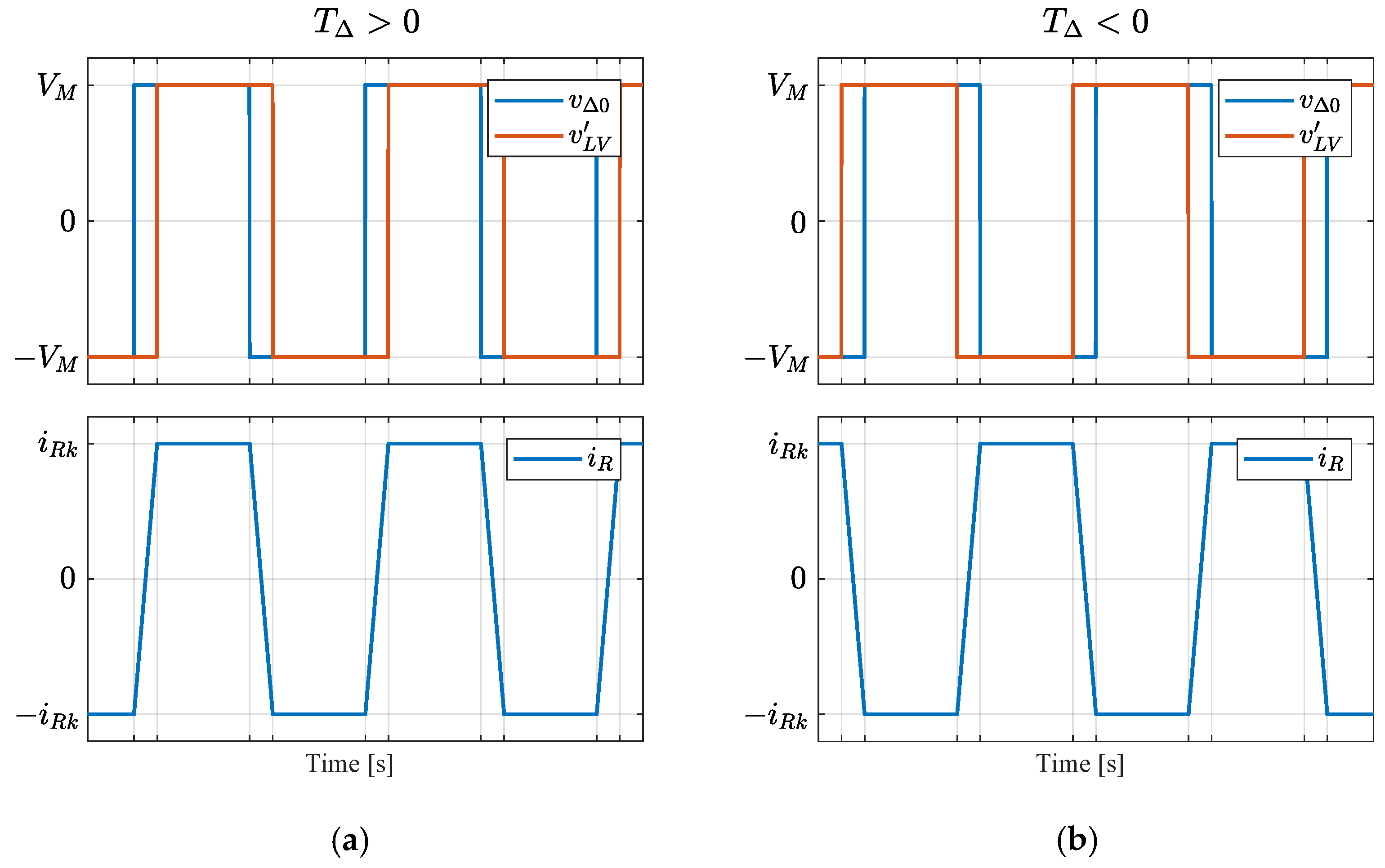
Figure 6 shows, with respect to the square wave voltages, the relation between the current value used by the control algorithm and the voltages phase shifts.
5. Numerical Results
The proposed control strategy has been tested in the Matlab/Simulink® environment; the simulation parameters are shown in Table 1.
In order to test the effectiveness of the used approach, the system undergoes two strong perturbations.
At 0.5 s, starting from a steady state no load condition, the power absorbed by the LV DC-Link varies instantaneously from 0 to 100 kW.
At 1.5 s, the power absorbed by the LV DC-Link varies instantaneously from 100 kW to −100 kW.
Figure 7 shows the whole simulation results. It can be noted that both the grid and the transformer powers accurately follow their reference. The ripple in the transformer power, averaged over the sampling time, is linked to the MMC homopolar differential voltage output, which is characterized by unwanted oscillations due to the differential currents control. The effective tracking of the reference powers allows a good dynamic response of the DC-Link controllers, as synthetically shown in the correspondence of the power step variation in correspondence of the second perturbation by the DC-Link overshot, contained under 4% of its rated value. The balancing of the DC-Link capacitors operates with satisfying results: the maximum voltage difference per leg is kept around 1% of the cells’ rated voltage during the whole simulation, except for the first step variation, when the maximum difference is characterized by a strong overshoot of about 8%, quickly recovering under 0.1 s. Finally, the RMS value of the transformer current is close enough to the ideal value (1 p.u.) obtained with an ideal square wave switching with no phase shift delay.
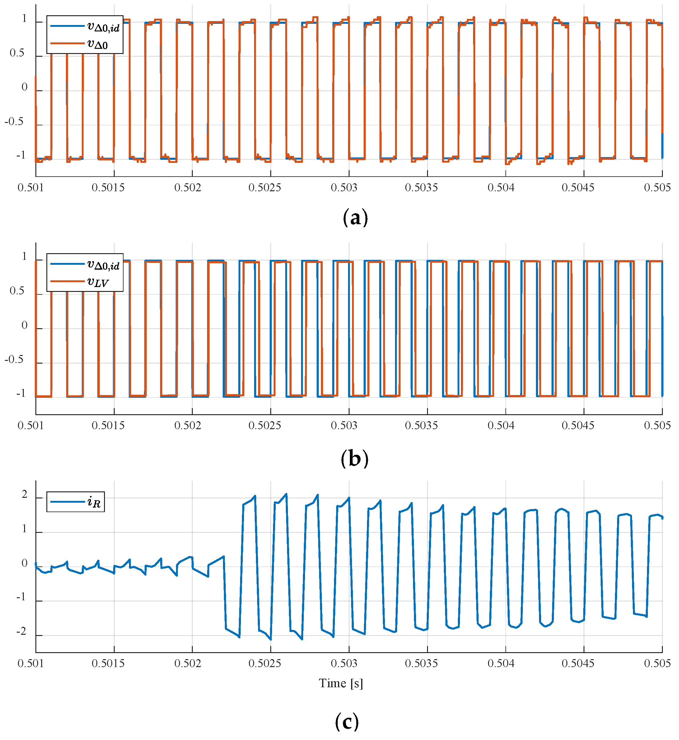
Figure 8 and Figure 9 show the behavior of the homopolar differential voltage and of the transformer currents in correspondence of the two power step variations. The voltages are expressed in p.u. of their rated values, whereas the transformer current is normalized with respect to the magnitude value obtainable with an ideal square-wave current in phase with the MMC ideal output voltage which would produce a power flow of . It can be noted that the output voltage is characterized by square shaped oscillations around its mean value (i.e., the ideal square-wave voltage of the PSC strategy) due to the asymmetrical switching of the upper and lower converters. This unwanted ripple forces the transformer current to deviate from its ideal shape (see Figure 3). The resulting interaction between and introduces the observed ripple in the transformer power. Finally, it can be noted that the phase shift between and quickly changes from a small value to a positive value in correspondence of the first step variation (see middle diagram in Figure 8) and from a positive value to a negative value in correspondence to the second step variation (see middle diagram in Figure 9).
6. Conclusions
In this paper, a Power Electronic Transformer topology for a 3-phase AC distribution grid is presented. In particular, an MMC topology is adopted for the MV side, whereas a Full-Bridge converter is used for the LV side. The control variables and their influence on the MMC operating conditions have been highlighted by using a space vector–based model.
While the PET power flow has been controlled by using a conventional PSC approach, the modulation of the MV stage has been properly modified in order to achieve an effective balancing of the MMC modules and to output a quasi-square-wave voltage at the primary side of the HF transformer.
The simulation results have confirmed the effectiveness of the proposed approach with the maximum unbalancing of the MMC DC-Link voltages being kept at reasonable levels.
The implemented modulation represents, therefore, another step toward the realization and the development of a 100 kVA PET prototype, to be presented in a future paper.
Acknowledgments
This work was developed thanks to the support of the financial programme PON03PE_00178_1—M.I.C.C.A. “Microgrid Ibride in Corrente Continua ed in corrente Alternata”.
Author Contributions
Gianluca Brando ported in C-Language the control algorithm; Biagio Bova performed the simulation analysis; Andrea Cervone wrote the system model; Adolfo Dannier sized the system parameters; Andrea Del Pizzo wrote the paper.
Conflicts of Interest
The authors declare no conflict of interest.
References
- Panwara, N.L.; Kaushikb, S.C.; Kotharia, S. Role of renewable energy sources in environmental protection: A review. Renew. Sustain. Energy Rev. 2011, 15, 1513–1524. [Google Scholar] [CrossRef]
- Üney, M.Ş.; Çetinkaya, N. Comparison of CO2 emissions fossil fuel based energy generation plants and plants with Renewable Energy Source. In Proceedings of the 2014 6th International Conference on Electronics, Computers and Artificial Intelligence (ECAI), Bucharest, Romania, 23–25 October 2014; pp. 29–34. [Google Scholar]
- Kang, M.; Enjeti, P.N. Analysis and design of electronic transformers for electric power distribution system. IEEE Trans. Power Electron. 1999, 14, 1133–1141. [Google Scholar] [CrossRef]
- Ronan, E.R.; Sudhoff, S.D.; Glover, S.F.; Galloway, D.L. A power electronic-based distribution transformer. IEEE Trans. Power Deliv. 2002, 17, 537–543. [Google Scholar] [CrossRef]
- Krishnaswami, H.; Ramanarayanan, V. Control of high-frequency AC link electronic transformer. IEE Proc. Electr. Power Appl. 2005, 152, 509–516. [Google Scholar] [CrossRef]
- Brando, G.; Dannier, A.; del Pizzo, A.; Rizzo, R. A High Performance Control Technique of Power Electronic Transformers in Medium Voltage Grid-Connected PV Plants. In Proceedings of the 19th International Conference on Electrical Machines (ICEM 2010), Rome, Italy, 6–8 September 2010; pp. 1–6. [Google Scholar]
- Brando, G.; Dannier, A.; del Pizzo, A.; Rizzo, R. Power Electronic Transformer for Advanced Grid Management in Presence of Distributed Generation. Int. Rev. Electr. Eng. 2011, 6, 3009–3015. [Google Scholar]
- Lai, J.S.; Maitra, A.; Mansoor, A.; Goodman, F. Multilevel intelligent universal transformer for medium voltage applications. In Proceedings of the IEEE 40th IAS Annual Meeting Industry Applications Conference, Hong Kong, China, 2–6 October 2005; Volume 3, pp. 1893–1899. [Google Scholar]
- Brando, G.; Dannier, A.; Rizzo, R. Power Electronic Transformer application to Grid-connected Photovoltaic Systems. In Proceedings of the International Conference on Clean Electrical Power (ICCEP’09), Capri, Italy, 9–11 June 2009; pp. 685–690. [Google Scholar]
- Dannier, A.; Rizzo, R. An overview of Power Electronic Transformer: Control strategies and topologies. In Proceedings of the International Symposium on Power Electronics Power Electronics, Electrical Drives, Automation and Motion, Sorrento, Italy, 20–22 June 2012; pp. 1552–1557. [Google Scholar]
- Briz, F.; Lopez, M.; Rodriguez, A.; Arias, M. Modular Power Electronic Transformers. IEEE Ind. Electron. Mag. 2016, 10, 6–19. [Google Scholar] [CrossRef]
- Briz, F.; López, M.; Rodríguez, A.; Zapico, A.; Arias, M.; Díaz-Reigosa, D. MMC based SST. In Proceedings of the IEEE 13th International Conference on Industrial Informatics (INDIN), Cambridge, UK, 22–24 July 2015. [Google Scholar]
- Yang, Y.; Mao, C.; Wang, D.; Tian, J.; Yang, M. Modeling and Analysis of the Common Mode Voltage in a Cascaded H-Bridge Electronic Power Transformer. Energies 2017, 10, 1357. [Google Scholar] [CrossRef]
- Gu, C.; Zheng, Z.; Xu, L.; Wang, K.; Li, Y. Modeling and Control of a Multiport Power Electronic Transformer (PET) for Electric Traction Applications. IEEE Trans. Power Electron. 2016, 31, 915–927. [Google Scholar] [CrossRef]
- Zhao, B.; Song, Q.; Li, J.; Wang, Y.; Liu, W. High-Frequency-Link Modulation Methodology of DC–DC Transformer Based on Modular Multilevel Converter for HVDC Application: Comprehensive Analysis and Experimental Verification. IEEE Trans. Power Electron. 2017, 32, 3413–3424. [Google Scholar] [CrossRef]
- Ilves, K.; Harnefors, L.; Norrga, S.; Nee, H.P. Predictive sorting algorithm for modular multilevel converters minimizing the spread in the submodule capacitor voltages. IEEE Trans. Power Electron. 2015, 30, 440–449. [Google Scholar] [CrossRef]
- Sathishkumar, P.; Himanshu; Piao, S.; Khan, M.A.; Kim, D.; Kim, M.; Jeong, D.; Lee, C.; Kim, H. A Blended SPS-ESPS Control. DAB-IBDC Converter for a Standalone Solar Power System. Energies 2017, 10, 1431. [Google Scholar] [CrossRef]
- Oliveira, R.; Yazdani, A. An Enhanced Steady-State Model and Capacitor Sizing Method for Modular Multilevel Converters for HVDC Applications. IEEE Trans. Power Electron. 2017, PP, 1. [Google Scholar] [CrossRef]
- Da Silva, S.A.O.; Coelho, E.A.A. Analysis and Design of a Three-Phase PLL Structure for Utility Connected Systems under Distorted Utility Conditions; CIEP: Sèvres, France, 2004. [Google Scholar]
- Siemaszko, D. Fast sorting method for balancing capacitor voltage in modular multilevel converters. IEEE Trans. Power Electron. 2015, 30, 463–470. [Google Scholar] [CrossRef]
Figure 1.
System topology of the proposed Power Electronic Transformer (PET) architecture.

Figure 2.
Equivalent circuit of the Modular Multilevel Converter (MMC)-based PET.

Figure 3.
Ideal Phase-Shift Control (PSC) with Square Wave Modulation (SQM) waveforms.

Figure 4.
Ideal switching waveforms of a single phase for a two modules MMC.

Figure 5.
Low voltage (LV)-side converter control scheme.

Figure 6.
Converter output voltages and transformer current for positive (a) and negative (b) power.
Figure 6.
Converter output voltages and transformer current for positive (a) and negative (b) power.

Figure 7.
Behavior of the actual/reference grid/transformer powers (a), the actual/reference LV/medium volt (MV) DC-Link voltages (b), maximum voltage difference per converters leg (c), transformer current RMS value (d).
Figure 7.
Behavior of the actual/reference grid/transformer powers (a), the actual/reference LV/medium volt (MV) DC-Link voltages (b), maximum voltage difference per converters leg (c), transformer current RMS value (d).

Figure 8.
Behavior in correspondence of 0 kW to 100 kW step variation of the actual MMC differential homopolar output compared with its mean value (a) of the transformer voltages (b) and of the transformer current (c).
Figure 8.
Behavior in correspondence of 0 kW to 100 kW step variation of the actual MMC differential homopolar output compared with its mean value (a) of the transformer voltages (b) and of the transformer current (c).

Figure 9.
Behavior in correspondence of 100 kW to −100 kW step variation of the actual MMC differential homopolar output compared with its mean value (a) of the transformer voltages (b) and of the transformer current (c).
Figure 9.
Behavior in correspondence of 100 kW to −100 kW step variation of the actual MMC differential homopolar output compared with its mean value (a) of the transformer voltages (b) and of the transformer current (c).


Table 1.
Simulation parameters.
| Symbol | Quantity | Value | Symbol | Quantity | Value |
|---|---|---|---|---|---|
| Sample Time Interval | 100 µs | Modulation Frequency | 5 kHz | ||
| Transformer Frequency | 5 kHz | System Rated Power | 100 kVA | ||
| Grid Rated Frequency | 50 Hz | Grid Rated Voltage | 20 kV | ||
| Modules per Leg | 9 | MV DC-Links Capacitance | 16 µF | ||
| Grid Boost Inductance | 0.5 H | MMC Inductance | 0.12 H | ||
| Power Transfer Inductance | 0.19 H | LV DC-Link Capacitance | 10 mF | ||
| Primary Boost Factor | 1.4 | Transformer Ratio | 50 |
© 2018 by the authors. Licensee MDPI, Basel, Switzerland. This article is an open access article distributed under the terms and conditions of the Creative Commons Attribution (CC BY) license (http://creativecommons.org/licenses/by/4.0/).
Share and Cite
MDPI and ACS Style
Brando, G.; Bova, B.; Cervone, A.; Dannier, A.; Del Pizzo, A. A Distribution Power Electronic Transformer with MMC. Appl. Sci. 2018, 8, 120. https://0-doi-org.brum.beds.ac.uk/10.3390/app8010120
AMA Style
Brando G, Bova B, Cervone A, Dannier A, Del Pizzo A. A Distribution Power Electronic Transformer with MMC. Applied Sciences. 2018; 8(1):120. https://0-doi-org.brum.beds.ac.uk/10.3390/app8010120
Chicago/Turabian StyleBrando, Gianluca, Biagio Bova, Andrea Cervone, Adolfo Dannier, and Andrea Del Pizzo. 2018. "A Distribution Power Electronic Transformer with MMC" Applied Sciences 8, no. 1: 120. https://0-doi-org.brum.beds.ac.uk/10.3390/app8010120
Note that from the first issue of 2016, this journal uses article numbers instead of page numbers. See further details here.