A Phase Change Material for Reconfigurable Circuit Applications

Department of Electrical and Computer Engineering, Marquette University, Milwaukee, WI 53233, USA
*
Author to whom correspondence should be addressed.
Appl. Sci. 2018, 8(1), 130; https://0-doi-org.brum.beds.ac.uk/10.3390/app8010130
Submission received: 12 December 2017
/
Revised: 6 January 2018
/
Accepted: 8 January 2018
/
Published: 18 January 2018
Abstract
:The large resistance contrast between amorphous and crystalline states of phase change materials (PCM) makes them a promising candidate for data-storage applications. Germanium telluride (GeTe), an early member of the PCM family, shows ~6 orders of magnitude difference in resistivity upon phase transition. In this paper, two different heating methods, direct (Joule) and indirect thermal heating, were applied to induce a phase transition in vertical and horizontal GeTe resistors. In the electrical measurements, it was observed that thermal heating produces a two orders of magnitude larger difference in GeTe resistivity that the Joule heating, irrespective of the resistor’s geometry and orientation. It was also found that the large inter-electrode distances in horizontal resistors make them impractical for low voltage applications. In addition, a correlation in between crystallization voltage and resistor’s geometrical parameters (i.e., inter-electrode distance and cross-sectional area) was also established. Here, it was found that the threshold voltage increases with resistor length, while it remains unaffected with a change in cross-sectional area. This work provides design guidelines to make use of not only GeTe but also other phase change materials in reconfigurable circuit applications.
1. Introduction
Temperature-induced amorphous and crystalline states of a phase change material (PCM) possess two distinct energy band structures; hence, they have different physical and chemical properties [1]. One such property is reflectivity, which has been utilized in the optical storage industry for storing data in the form of CDs and DVDs [2]. Similarly, a large difference (4–6 orders of magnitude) in resistance (hence the resistivity) values in amorphous and crystalline phases of a PCM is the basis for next generation non-volatile memory applications [3]. Furthermore, the ability to switch from a highly resistive amorphous state (OFF) to a highly conductive crystalline state (ON) or vice-versa makes PCM an ideal candidate for radio-frequency (RF) switching applications [4]. In previous works, thermal-induced reversible phase transition has been demonstrated in several chalcogenide compounds such as germanium antimony telluride (GeSbTe or GST), and germanium telluride (GeTe) [4,5,6]. For example, Redaelli et al. demonstrate Joule heating induced phase transition in GST electronic memory cells of size ~0.80 µm × 0.40 µm × 60 nm and concluded that the threshold switching in such devices does not depend on structural changes [7]. In fact, it was an outcome of competition between trap-assisted carrier recombination and field-assisted carrier generation. In the same work, it was also observed that the PCM crystallization depends not only on the magnitude but also on the duration of applied current pulse [7]. However, poor thermal stability in amorphous phase GST and void formation due to volume shrinkage upon crystallization limit the GST application range [8]. In comparison to GST, GeTe has several advantages including higher stability in amorphous phase, ultra-fast reversible phase transition (µs–to crystallize and ns–to amorphized), and higher OFF/ON resistivity ratio. All these superior properties make GeTe a leading candidate for memory, as well as RF switching applications [9]. The main advantages of GeTe RF switches over the conventional microelectromechanical systems (MEMS) electrostatic switches (of the same size) are, including but not limited to the simpler fabrication method, long lifetime, large cut-off frequency (in THz), near zero in-state power consumption/lower switching voltages, high power handling capabilities, immune to radiation exposure (good for space applications), and the elimination of special packaging requirements [9,10,11,12,13]. Furthermore, the simpler design allows the integration of GeTe switches with various MEMS and CMOS devices.
As the properties of PCM depend on the nature of the transition (sharpness, duration etc.), it is important to understand the phase change mechanism for fabricating the GeTe RF switches of desired properties. The transition between insulating (amorphous) and conducting (crystalline) phases is usually induced by heating and cooling the PCM resistor. When room temperature-grown PCM (in amorphous phase) is heated uniformly above its glass temperature (Tg), crystallization occurs. In the case of GeTe thin films, crystallization starts with the growth of small nuclei followed by their continuous expansion until they merge with other crystal sites to form larger crystals [14]. On the other hand, the transition from the crystalline to the amorphous phase occurs upon quenching the PCM material from its melting point (TM). The quenching/heating rate, minimum/maximum temperature, heating methods, and even the device size and geometry are some of the parameters that decide the switching time and behavior. Two most common heating methods, Joule and indirect thermal heating, are in use to induce phase transition in GeTe devices [15]. In the indirect heating method, a separate resistive heater near to the PCM resistor provides enough heat for the phase transition, whereas Joule heating involves drawing current directly through the PCM.
In this paper, we fabricated vertical and horizontal GeTe resistors of various dimensions, with the resistor length ranging from 0.09 to 10 µm and the cross-sectional area varying from 0.45 to 225 μm2. The major difference between this and previous works is in device geometry. For example, in this work the devices are relatively larger in size (e.g., minimum size is 3 µm × 3 µm × 100 nm) than the previously investigate devices [11]). In addition, our primary target application areas are DC and RF circuits and switching. All the thermal and electrical characterizations were done using a micromanipulator probe station (with thermal chuck) in conjunction with an Agilent 34410A multimeter and Agilent 33250A waveform generator (Keysight Technologies (former Agilent), Santa Rosa, CA, USA). A relationship in between device geometrical parameters and threshold voltage (so the transition temperature) is established where voltage increases with inter-electrode distance but remains constant with the area. Such a relationship reveals a significant difference in transition temperature obtained by direct (i.e., Joule) and indirect thermal heating, which further suggests the impracticality of horizontal devices (i.e., with large inter-electrode distance) in low voltage applications. Furthermore, this work reveals the limitation of Joule heating in inducing reverse transition (i.e., crystalline to amorphous) in large size devices.
2. Design and Fabrication
2.1. Vertical and Horizontal Resistor Designs
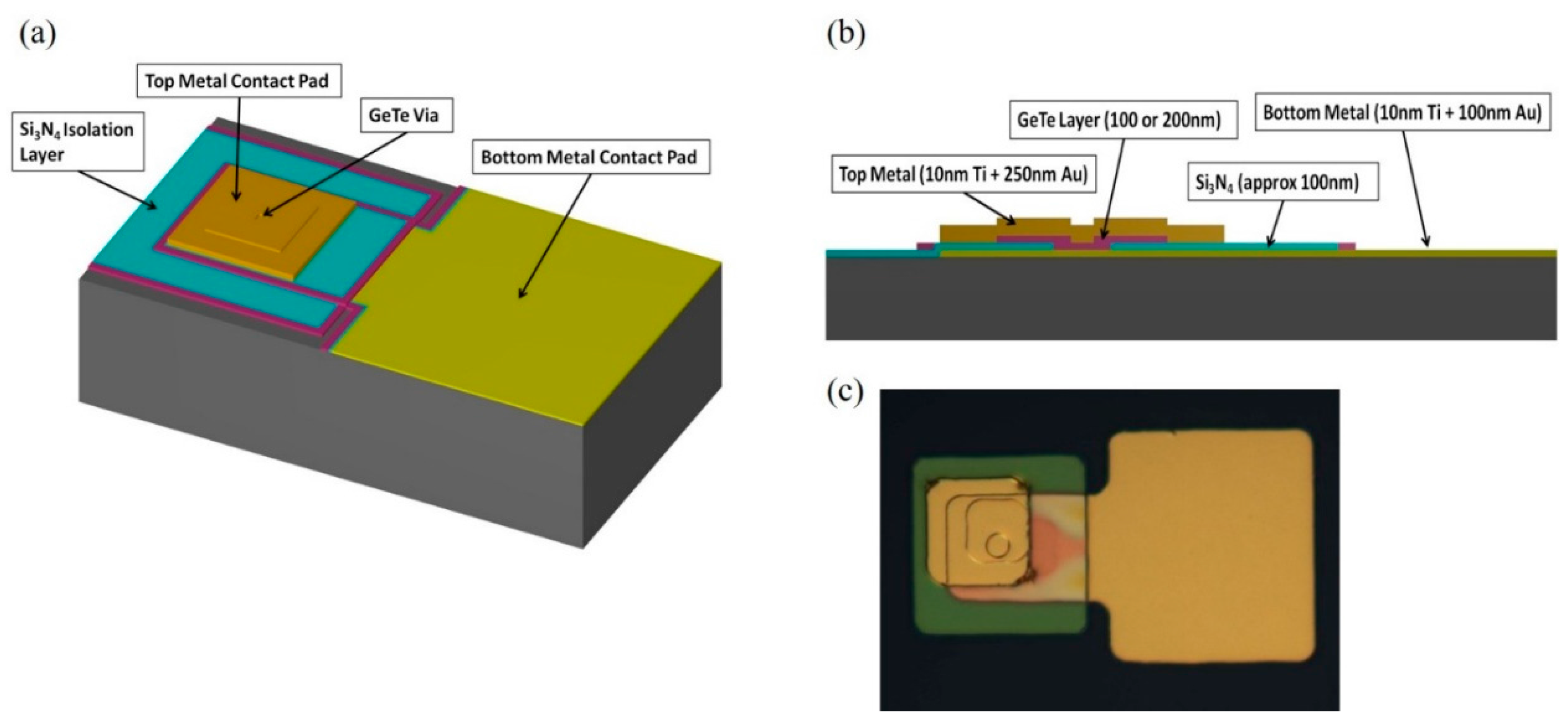
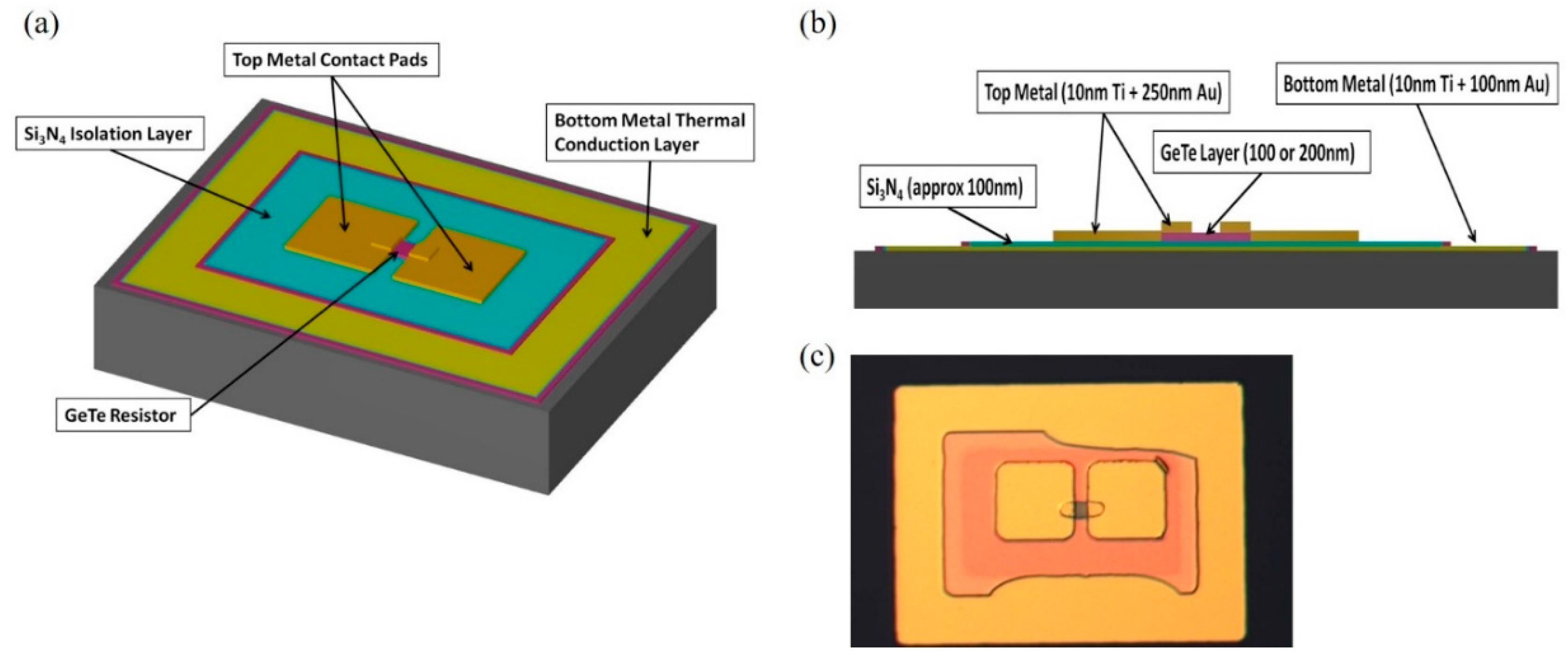
The device schematics of vertical and horizontal GeTe resistors are shown in Figure 1 and Figure 2, respectively. Figure 1a shows the top view of a vertical resistor containing a GeTe thin layer sandwiched between two gold contacts. These metal contacts are electrically isolated from each other by a 100-nm thick Si3N4 film (Figure 1b). The optical microscope image of a ‘ready to test’ vertical resistor is shown in Figure 1c. Here, via hole is at the location where the GeTe thin film connects from the top and to bottom electrodes. Figure 1c shows that the top metal contact completely covers the whole via hole despite some misalignment. Therefore, we believe this slight misalignment is more cosmetic in nature and does not adversely affect the transport characteristics. In comparison to vertical devices, the horizontal resistors consist of a narrow bridge of GeTe connecting two gold contact pads as shown in Figure 2a. Similar to a vertical resistor, a Si3N4 layer separates top gold contact pads from the bottom conduction layer (Figure 2b). This bottom conduction layer is essential for fast heat dissipation during the melt-quench process and to promote uniform crystallization. The optical microscope image of a ‘ready to test’ horizontal resistor is shown in Figure 2c. Irrespective of design, the resistance of all the resistors can be expressed by
where ρ is GeTe resistivity, L the inter-electrode distance, and A the cross-sectional area of the testing resistor. Here, it is noteworthy to mention that ‘L’ represents GeTe layer thickness and separation between two gold pads in vertical and horizontal configuration, respectively. Similarly, ‘A’ represents the size of the via and the product of the GeTe layer thickness with the distance between the contact pads for vertical and horizontal resistors, respectively. Here, each design size was linearly scaled to maintain the measurement consistency and to establish a relationship between phase transition and voltage pulse. Vertical resistors had cross-sectional areas ranging from 3 × 3 μm2 to 15 × 15 μm2 with 90 nm, 150 nm, and 400 nm interelectrode distances. On the other hand, horizontal resistors have cross-sectional areas ranging from 5 × 0.09 μm2 to 10 × 0.4 μm2 with inter-electrode distances of 5 μm and 10 μm.
2.2. Fabrication Process
All the resistors were fabricated using a 4-mask/4-layer process. All resistors were fabricated on B-doped Si wafers by Ultraviolet (UV)-photolithography processes. All the wafers were first cleaned with organic solvents to remove grease and metallic impurities. The bottom metal layer consisting 10 nm Ti and 100 nm Au was deposited using e-beam evaporation. The unwanted material was removed by lift-off process in hot acetone (~80 °C). Next, 100 nm thick Silicon Nitride (Si3N4) layer was grown on top of bottom Au contact pad using plasma enhanced chemical vapor deposition (PECVD). For vertical resistors, Reactive Ion Etching (RIE) was performed to pattern the via holes in the Si3N4 layer. A high vacuum RF sputtering of GeTe (99.999% purity) target was done to deposit GeTe thin films of desired thickness. Finally, e-beam metal evaporation and lift-off processes were used to deposit and pattern the top contact pads consisting of 10 nm Ti and either 250 nm or 400 nm Au, depending on the GeTe film thickness.
3. Experimental Results
The room temperature (RT) deposition of GeTe thin layers keeps the fabricated resistors in the amorphous state. The change in amorphous state resistance with GeTe layer thickness for horizontal and vertical resistors is shown in Figure 3. Since the focus of this work is to emphasize DC/RF circuit and switching applications, it makes good sense to use device parameters like resistance and S-parameters instead of material properties like resistivity. In our experimental limits, the horizontal resistors were found more resistive than the vertical ones. Such behavior can be attributed to large inter-electrode distance and small cross-sectional area of horizontal resistors. Here, an increment in GeTe layer thickness increases the effective cross-sectional area, which further leads to a reduction in horizontal resistor’s resistivity. For example, 5 × 5 μm2 device resistance decreases from ~1 GΩ to 10 MΩ (corresponding resistivity change is from ~2.0 × 10⁷ to 5.0 × 10⁵ Ω-cm) as GeTe layer thickness increases from 100 to 400 nm. On the other hand, the resistance of vertical devices increases nearly by an order of magnitude upon increasing GeTe layer thickness. For example, resistance changes from 1.0 × 10⁴ Ω to 8.0 × 10⁴ Ω (resistivity changes from 1.2 × 10³ to 1.4 × 10⁴ Ω-cm) as 10 × 10 μm2 device thickness increases from 100 to 400 nm. Such behavior can also be explained by Equation (1), in which GeTe thickness determines the inter-electrode distance. Therefore, the resistivity of vertical resistors increases with GeTe layer thickness. Overall, device geometry is one of the main factors for fine tuning the device resistance. For example, a 10 × 0.4 × 10 μm3 horizontal resistor (where A = 4 μm2 and L = 10 μm) would have at least 2 orders of magnitude larger resistance than a 10 × 10 × 0.4 μm3 vertical resistor, where A = 100 μm2 and L= 0.4 μm, despite having the same device volume (Figure 3).
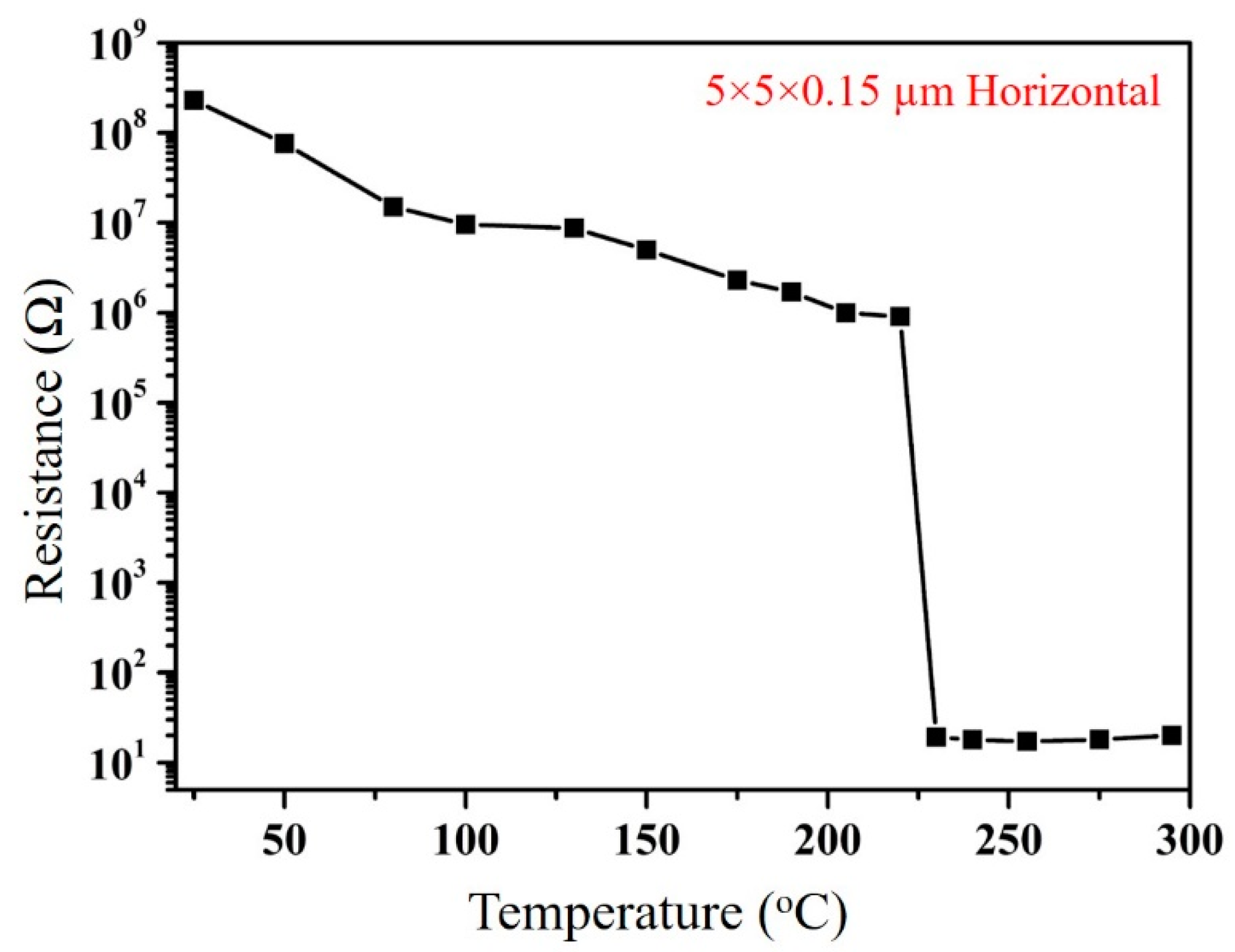
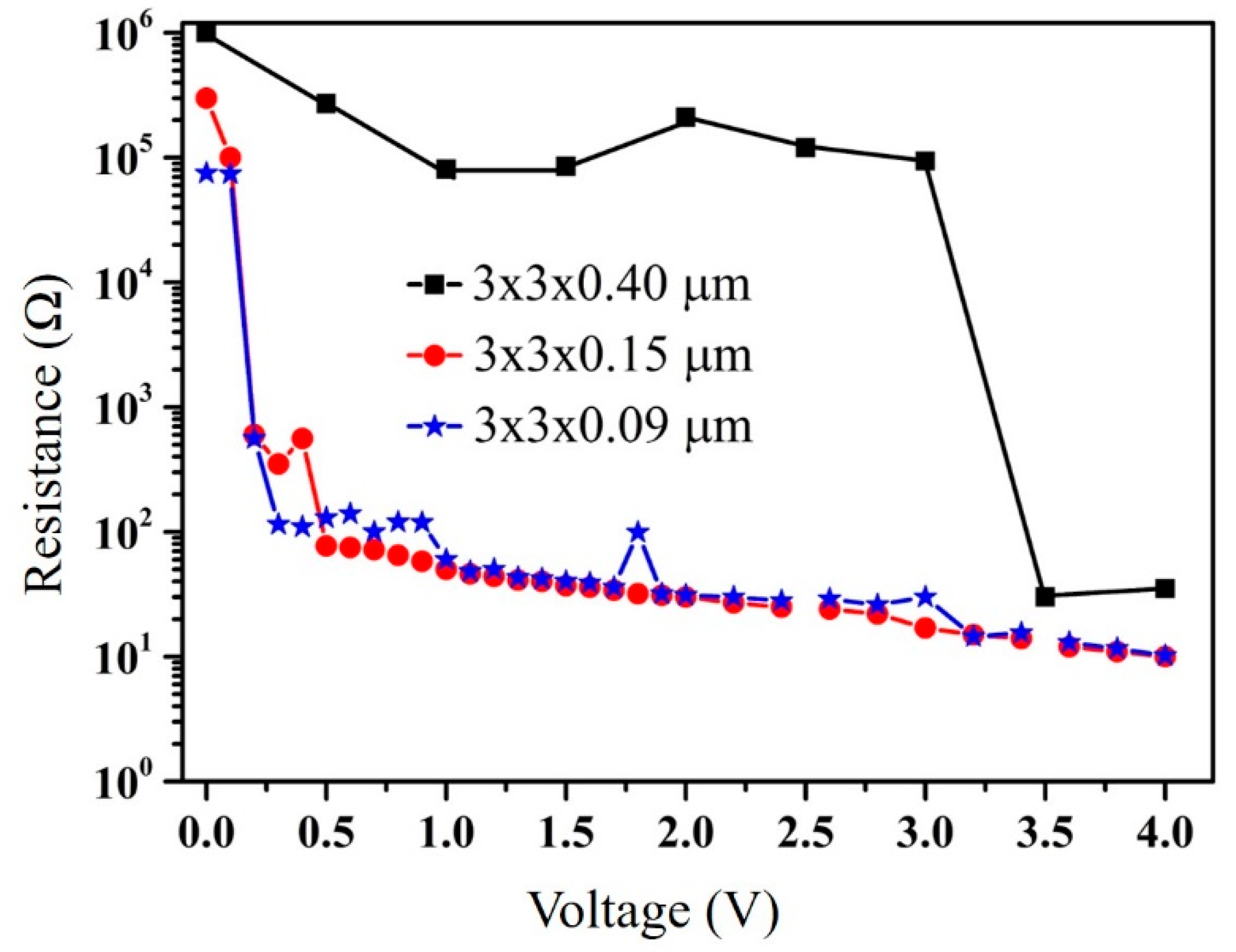
After characterizing amorphous GeTe resistors, two different heating methods, (1) thermal conduction, and (2) Joule heating, were applied to initiate amorphous to crystalline state phase transition. In the thermal conduction mechanism, resistors were mounted on a thermal chuck and resistance was measured with increasing temperature. The resulting plot of a horizontal resistor (5 × 5 × 0.15 µm3) is shown in Figure 4. A steady reduction in resistance value (from few ‘hundred MΩ’ to ‘few MΩ’) with increasing temperature (from RT to 220 °C) was recorded. Such behavior was attributed to the thermally activated charge carriers those increase with temperature. An abrupt drop in resistance was observed at 220 °C < T < 230 °C. This large resistance change (few MΩ to few Ω) in 10 °C temperature window confirms amorphous to crystalline phase transition. A similar phase transition was observed for vertical devices but with a small initial resistance (not shown here). Similar results can be obtained by Joule heating where an electrical current passing through GeTe resistor increases the temperature of the device and induces the phase transition. The experimental demonstration of Joule heating-induced phase transition is shown in Figure 5, in which three vertical resistors of same via holes (3 × 3 µm2) but different GeTe thickness (0.09 to 0.40 µm) are tested. The average change in resistance versus applied voltage plot of these resistors is shown in Figure 5. The resistors with thinner GeTe (0.09 and 0.15 µm) show amorphous to crystalline transition at a small voltage pulse of magnitude ~0.50 V. However, a large voltage pulse (~3.25 V) was required to induce a phase transition in the thicker resistor (0.40 µm). As the phase transition in PCM devices is quire sharp, a voltage drop across the resistors was measured using a current source for accurate explanation of such transition. However, this method was not found adequate to capture the abrupt transition. Therefore, we plan to use high speed oscilloscope to capture the precise transition times exhibited by these novel devices in our future work. Furthermore, similar to Krebs et al., we also used to obtain threshold field values from threshold voltage [16]. Here, it is observed that Et increases from 3.30 V/µm to 8.13 V/µm as GeTe layer thickness increases from 90 nm to 400 nm. On the other hand, horizontal devices show such phase transition at relatively higher threshold voltage (30–100 V) due to the presence of larger inter-electrode distance (5 and 10 µm). Here, Et varies from ~6.0 V/µm to 10 V/µm as channel length increases. An important relationship between threshold voltage, threshold field and inter-electrode distance can be established; resistors with large inter-electrode distance require higher threshold voltage, hence the larger threshold field for the phase transition.
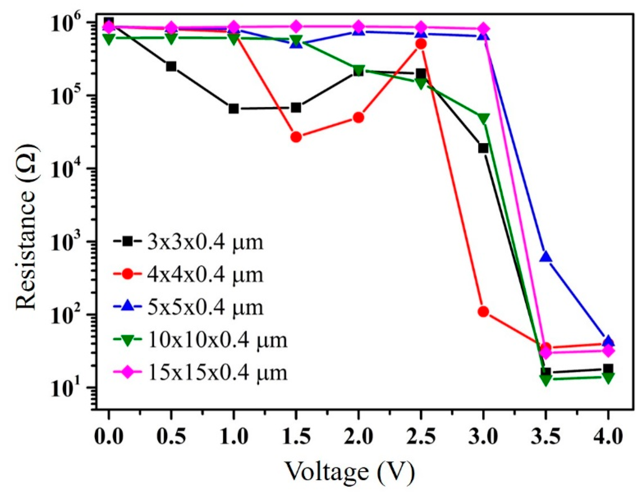
After establishing the above relationship, the impact of device cross-sectional area on threshold voltage was also investigated. Various resistors of the different area but same inter-electrode distance were tested using a probe station. Figure 6 shows the average resistance change versus threshold voltage plot of tested resistors. It was observed that all the resistors (except one) demonstrate amorphous to crystalline phase transition at ~3.20 V. The independence of threshold voltage on the resistor’s cross-sectional area can be attributed to bottom conduction layer, which assures a uniform Joule heating in GeTe resistors. Therefore, using a relationship between heat intensity (I) and power (P) i.e., (where V is the effective conduction volume and can be given as product of area A and channel length L), one can obtain , which is independent of the cross-sectional area. This explanation suggests that the fluctuating resistance of device of size 4 × 4 × 0.40 µm3 can be attributed to unstable contacts. Similar behavior was observed for horizontal devices (results not shown here).
Here, it is noteworthy that the Figure 4 shows the indirect heating (i.e., hot plate)-induced phase transition in a horizontal PCM resistor (Temperature on X-axis), whereas Figure 5 and Figure 6 corresponds to Joule heating (i.e., current flow)-induced phase transition in vertical resistors. As in the Joule heating case, device temperature is increased by applying external voltage, and the measured resistance is given as a function of applied voltage not applied temperature.
4. Discussion
In this work, vertical and horizontal GeTe resistors were fabricated and characterized. It was observed that extremely small (few nm) inter-electrode distance in vertical resistors makes them suitable for low power applications and ultra-small devices. On the other hand, horizontal resistors were easier to fabricate and more useful in relatively larger devices. Experimental results confirmed that threshold voltage in both geometries can be tuned just by changing the thickness of GeTe layer (i.e., inter-electrode distance). However, the independence of threshold voltage on the cross-sectional area can be attributed to the nucleation sites forming in the amorphous phase. Such sites provide a low resistance path for current conduction, which stops the crystallization process. This is an inherent drawback of the direct heating method and can be avoided by indirect heating.
The reverse crystalline to amorphous phase transition process is much more complicated due to the need of rapid cooling from GeTe melting temperature. This transition can be obtained by voltage pulsing, but the presence of crystalline seeds, resulting from the melt-quench process, reduces the OFF-state resistance. In this work, the reverse phase transition experiments failed due to instrument limitations, e.g., interference from voltage source meter (resulting undesired phase change) and inability to achieve fast enough quenching rate. Wen et al. suggested using a voltmeter in conjunction with a separate current source meter to resolve the first issue [17]. Therefore, it is with certain modifications in our experimental setup that we will be able to demonstrate crystalline to an amorphous phase transition.
5. Conclusions
In this work, we demonstrated the utility of phase change resistors for reconfigurable circuits. Amorphous GeTe resistors of different dimensions and geometries were fabricated by photolithography processes. The resistance of as-deposited resistors varies from few kΩ to several MΩ depending primarily on inter-electrode distance. Heat-induced crystallization showed a six order of magnitude change in resistance. However, crystallization by Joule heating showed a four order of magnitude change in resistance. It was also observed that the threshold voltage increases with inter-electrode distance, while remains unaffected with a change in cross-sectional area. In addition, it can also be concluded that the vertical resistors are preferable for low voltage applications due to the small GeTe layer thickness, hence the small inter-electrode distances. Same order of threshold voltage can induce a phase transition in horizontal resistors but that require more specialized fabrication processes (i.e., e-beam lithography). This work provides interesting insight on the use of GeTe in reconfigurable device application and will be applicable to other PCM as well.
Acknowledgments
The authors thank the Air Force Office of Scientific Research (AFOSR) for funding this research, and Brent Danner, Alex Gwin, Christopher Kodama, and James Sattler for their participation.
Author Contributions
Dushyant Tomer compiled and edited the final manuscript. Ronald A. Coutu, Jr. conceived the original research idea, proposed the specific project to AFOSR, led the design, fabrication, testing, and data collection efforts, mentored numerous graduate student projects, and edited the final manuscript.
Conflicts of Interest
The authors declare no conflict of interest.
References
- Raoux, S.; Welnic, W.; Ielmini, D. Phase change materials and their applications in nonvolatile memories. Chem. Rev. 2010, 110, 240–267. [Google Scholar] [CrossRef] [PubMed]
- Wuttig, M.; Yamada, N. Phase-change materials for rewriteable data storage. Nat. Mater. 2007, 6, 824–832. [Google Scholar] [CrossRef] [PubMed]
- Ielmini, D.; Lacaita, A.L. Phase change materials in non-volatile storage. Mater. Today 2011, 14, 600–607. [Google Scholar] [CrossRef]
- Shim, Y.; Hummel, G.; Rais-Zadeh, M. RF switches using phase change materials. In Proceedings of the 2013 IEEE 26th International Conference on Micro Electro Mechanical Systems, Taipei, Taiwan, 20–24 January 2013; pp. 237–240. [Google Scholar]
- Sokolowski-Tinten, K.; Solis, J.; Bialkowski, J.; Siegel, J.; Afonso, C.N.; von der Linde, D. Dynamics of ultrafast phase changes in amorphous GeSb films. Phys. Rev. Lett. 1998, 81, 3679–3682. [Google Scholar] [CrossRef] [Green Version]
- Reifenberg, J.P.; Panzer, M.A.; Kim, S.; Gibby, A.M.; Zhang, Y.; Wong, S.; Wong, H.P.; Pop, E.; Goodson, K.E. Thickness and stochiometry dependence of the thermal conductivity of GeSbTe films. Appl. Phys. Lett. 2007, 91, 111904–111906. [Google Scholar] [CrossRef]
- Redaelli, A.; Pirovano, A.; Pellizzer, F.; Lacaita, A.L.; Ielmini, D.; Bez, R. Electronic Switching Effect and Phase-Change Transition in Chalcogenide Materials. IEEE Electron Device Lett. 2004, 25, 684–686. [Google Scholar] [CrossRef]
- Zhou, X.; Dong, W.; Zhang, H.; Simpson, R.E. A zero density change phase change memory material: GeTe-O structural characteristics upon crystallization. Sci. Rep. 2015, 5, 11150. [Google Scholar] [CrossRef] [PubMed]
- Bruns, G.; Merkelbach, P.; Schlockermann, C.; Salinga, M.; Wuttig, M.; Happ, T.D.; Philipp, J.B.; Kund, M. Nanosecond switching in GeTe phase change memory cells. Appl. Phys. Lett. 2009, 95, 043108. [Google Scholar] [CrossRef]
- Wang, M.; Rais-Zadeh, M. Development and evaluation of germanium telluride phase change material based Ohmic switches for RF applications. J. Micromech. Microeng. 2016, 27, 013001. [Google Scholar] [CrossRef]
- El-Hinnawy, N.; Borodulin, P.; Wagner, B.; King, M.R.; Mason, J.S.; Jones, E.B.; McLaughlin, S.; Veliadis, V.; Snook, M.; Sherwin, M.E.; et al. A four terminal, inline, chalcogenide phase change RF switch using an independent resistive heater for thermal actuation. IEEE Electron Device Lett. 2013, 34, 1313–1315. [Google Scholar] [CrossRef]
- Wang, M.; Shim, Y.; Rais-Zadeh, M. A low-loss directly heated two-port RF phase change switch. IEEE Electron Device Lett. 2014, 35, 491–493. [Google Scholar] [CrossRef]
- El-Hinnawy, N.; Borodulin, P.; Jones, E.B.; Wagner, B.P.; King, M.R.; Mason, J.S.; Hartman, J.; Howell, R.; Lee, M.; Young, R. Improvements in GeTe-based inline phase-change switch technology for RF switching applications. In Proceedings of the CS MANTECH Conference, Denver, CO, USA, 19–22 May 2014. [Google Scholar]
- Raoux, S.; Wuttig, M. Phase Change Materials Science and Applications; Springer Science + Business Media, LLC: New York, NY, USA, 2009; p. 11. [Google Scholar]
- Wen, C.Y.; Zhao, E.K.; Chong, T.C.; Bain, J.A.; Schlesinger, T.E.; Pileggi, L.T.; Paramesh, J. A phase-change via-reconfigurable on-chip inductor. In Proceedings of the IEEE International Electron Devices Meeting, San Francisco, CA, USA, 6–8 December 2010; pp. 10.3.1–10.3.4. [Google Scholar]
- Krebs, D.; Raoux, S.; Rettner, C.T.; Burr, G.W.; Salinga, M.; Wuttig, M. Threshold field of phase change memory materials measured using phase change bridge devices. Appl. Phys. Lett. 2009, 95, 082101. [Google Scholar] [CrossRef]
- Chua, E.K.; Shi, L.P.; Zhao, R.; Lim, K.G.; Chong, T.C.; Schlesinger, T.E.; Bain, J.A. Low resistance, high dynamic range reconfigurable phase change switch for radio frequency applications. Appl. Phys. Lett. 2010, 97, 183506–183508. [Google Scholar] [CrossRef]
Figure 1.
GeTe vertical resistor designs: L-Edit (a) top; and (b) side view of a resistor; (c) optical microscope image of vertical resistor with 3 µm diameter GeTe via hole.
Figure 1.
GeTe vertical resistor designs: L-Edit (a) top; and (b) side view of a resistor; (c) optical microscope image of vertical resistor with 3 µm diameter GeTe via hole.

Figure 2.
GeTe horizontal resistor designs: L-Edit (a) top; and (b) side view of a resistor; (c) optical microscope image of a resistor with 5 µm inter-electrode distance.
Figure 2.
GeTe horizontal resistor designs: L-Edit (a) top; and (b) side view of a resistor; (c) optical microscope image of a resistor with 5 µm inter-electrode distance.

Figure 3.
Amorphous phase resistance versus GeTe layer thickness plot for vertical and horizontal resistors.
Figure 3.
Amorphous phase resistance versus GeTe layer thickness plot for vertical and horizontal resistors.

Figure 4.
Temperature induced amorphous to crystalline phase transition in a horizontal GeTe resistor.
Figure 4.
Temperature induced amorphous to crystalline phase transition in a horizontal GeTe resistor.

Figure 5.
Effect of inter-electrode distance on Joule heating induced crystallization in GeTe vertical resistors (same cross-sectional area).
Figure 5.
Effect of inter-electrode distance on Joule heating induced crystallization in GeTe vertical resistors (same cross-sectional area).

Figure 6.
Effect of cross-sectional area on Joule heating-induced crystallization in GeTe vertical resistors (same inter-electrode distance).
Figure 6.
Effect of cross-sectional area on Joule heating-induced crystallization in GeTe vertical resistors (same inter-electrode distance).

© 2018 by the authors. Licensee MDPI, Basel, Switzerland. This article is an open access article distributed under the terms and conditions of the Creative Commons Attribution (CC BY) license (http://creativecommons.org/licenses/by/4.0/).
Share and Cite
MDPI and ACS Style
Tomer, D.; Coutu, R.A. A Phase Change Material for Reconfigurable Circuit Applications. Appl. Sci. 2018, 8, 130. https://0-doi-org.brum.beds.ac.uk/10.3390/app8010130
AMA Style
Tomer D, Coutu RA. A Phase Change Material for Reconfigurable Circuit Applications. Applied Sciences. 2018; 8(1):130. https://0-doi-org.brum.beds.ac.uk/10.3390/app8010130
Chicago/Turabian StyleTomer, Dushyant, and Ronald A. Coutu. 2018. "A Phase Change Material for Reconfigurable Circuit Applications" Applied Sciences 8, no. 1: 130. https://0-doi-org.brum.beds.ac.uk/10.3390/app8010130
Note that from the first issue of 2016, this journal uses article numbers instead of page numbers. See further details here.