Article

Imaging Material Texture of As-Deposited Selective Laser Melted Parts Using Spatially Resolved Acoustic Spectroscopy

Optics and Photonics Group, Faculty of Engineering, University of Nottingham, University Park, Nottingham NG7 2RD, UK
*
Author to whom correspondence should be addressed.
Submission received: 27 September 2018 / Revised: 17 October 2018 / Accepted: 18 October 2018 / Published: 19 October 2018
(This article belongs to the Special Issue Laser Ultrasonics)

Abstract

:
Additive manufacturing (AM) is a production technology where material is accumulated to create a structure, often through added shaped layers. The major advantage of additive manufacturing is in creating unique and complex parts for use in areas where conventional manufacturing reaches its limitations. However, the current class of AM systems produce parts that contain structural defects (e.g., cracks and pores) which is not compatible with certification in high value industries. The probable complexity of an AM design increases the difficulty of using many non-destructive evaluation (NDE) techniques to inspect AM parts—however, a unique opportunity exists to interrogate a part during production using a rapid surface based technique. Spatially resolved acoustic spectroscopy (SRAS) is a laser ultrasound inspection technique used to image material microstructure of metals and alloys. SRAS generates and detects `controlled’ surface acoustic waves (SAWs) using lasers, which makes it a non-contact and non-destructive technique. The technique is also sensitive to surface and subsurface voids. Work until now has been on imaging the texture information of selective laser melted (SLM) parts once prepared (i.e., polished with R a < 0.1 μ m)—the challenge for performing laser ultrasonics in-process is measuring waves on the rough surfaces present on as-deposited parts. This paper presents the results of a prototype SRAS system, developed using the rough surface ultrasound detector known as speckle knife edge detector (SKED)—texture images using this setup of an as-deposited Ti64 SLM sample, with a surface roughness of S a 6 μ m, were obtained.

Graphical Abstract

1. Introduction

Additive manufacturing (AM) is a production process used to form three dimensional structures in which material is deposited on top of an already set structure—commonly this is implemented by adding shaped layers. The method enables manufacturers to create parts that cannot be made using traditional fabrication methods such as machining, casting or forging. It also allows for rapid prototyping and complex near-net shape manufacture. For precision metal alloy manufacture, the powdered bed category of AM techniques is often identified as being able to produce parts that have intricate features.
Selective laser melting (SLM) is a technique where metal powder material is fused under a high power laser source [1]. Once a layer shape is formed, the bed is lowered and additional powder is applied using a re-coater. To prevent oxidisation and contamination, the build is performed inside an inert gas chamber (e.g., Argon). SLM machines give manufacturers the ability to finely control processes and environmental variables—production is controlled through laser scanning powers and pattern regimes, the gas flow in the enclosed build chamber environment, and the powder application rates. Since the additive manufacturing process is in its infancy, parts currently produced suffer from non-conformities which include incorrect part dimensions and inappropriate microstructure. Moreover, structures created suffer from manufacturing defects, which could include cracks and pores [2].
To find these problems, material inspection is required—however, the complex designs made possible through using AM present a challenge for standard contact-based measurement techniques. Simple visual inspection methods also do not provide sufficient information about the quality of the built part, as the key-holing phenomenon observed during manufacture (where a subsurface pore is created) would not be identified [3]. It is possible to characterise parts through destructive testing, which would provide statistical information based on AM build parameters [4], however, this indirect part information is undesirable to high performance part manufacturers. Post-production inspection is also possible—X-ray computer tomography (XCT) is a widely adopted technique for this purpose [5]. However, due to the method of manufacture, it is possible to use a surface-based non-destructive evaluation (NDE) techniques on each top layer as a structure is built—an in-situ inspection technique could be used to collect volumetric data of a part being built. Rapid measurements could be fed back into the system for reworking or in severe cases, scrapping builds to save material and time. Current areas of focus for in-situ AM inspection includes using purely optical measurement techniques to observe the surface topography and to find large surface breaking defects [6], and observing the melt-pool created when the feed material is locally heated to create the build structure [7].
In this paper, we present the laser ultrasonic inspection technique known as spatially resolved acoustic spectroscopy, or spatially resolved acoustic spectroscopy (SRAS) [8], for imaging texture and defects on additively manufactured components. The technique is non-contact, all optical and non-destructive. In previous work, we showed that it was possible to use SRAS to image the surface texture [9], and identify both surface and subsurface defects [10] on prepared samples made using SLM. In these cases, prepared samples were polished so that the surface roughness was R a < 100 nm. Results in this paper show our images, obtained using a prototype SRAS setup, of an as-deposited SLM Ti-6Al-4V (Ti46) sample with a surface roughness of S a 6 μ m (the R a and S a are measurements of the mean surface profile deviation along a line and area, respectively). To illustrate that a SRAS system could be implemented to provide in-situ AM measurements, we also report on our efforts to integrate a SRAS system into an SLM build chamber shell.

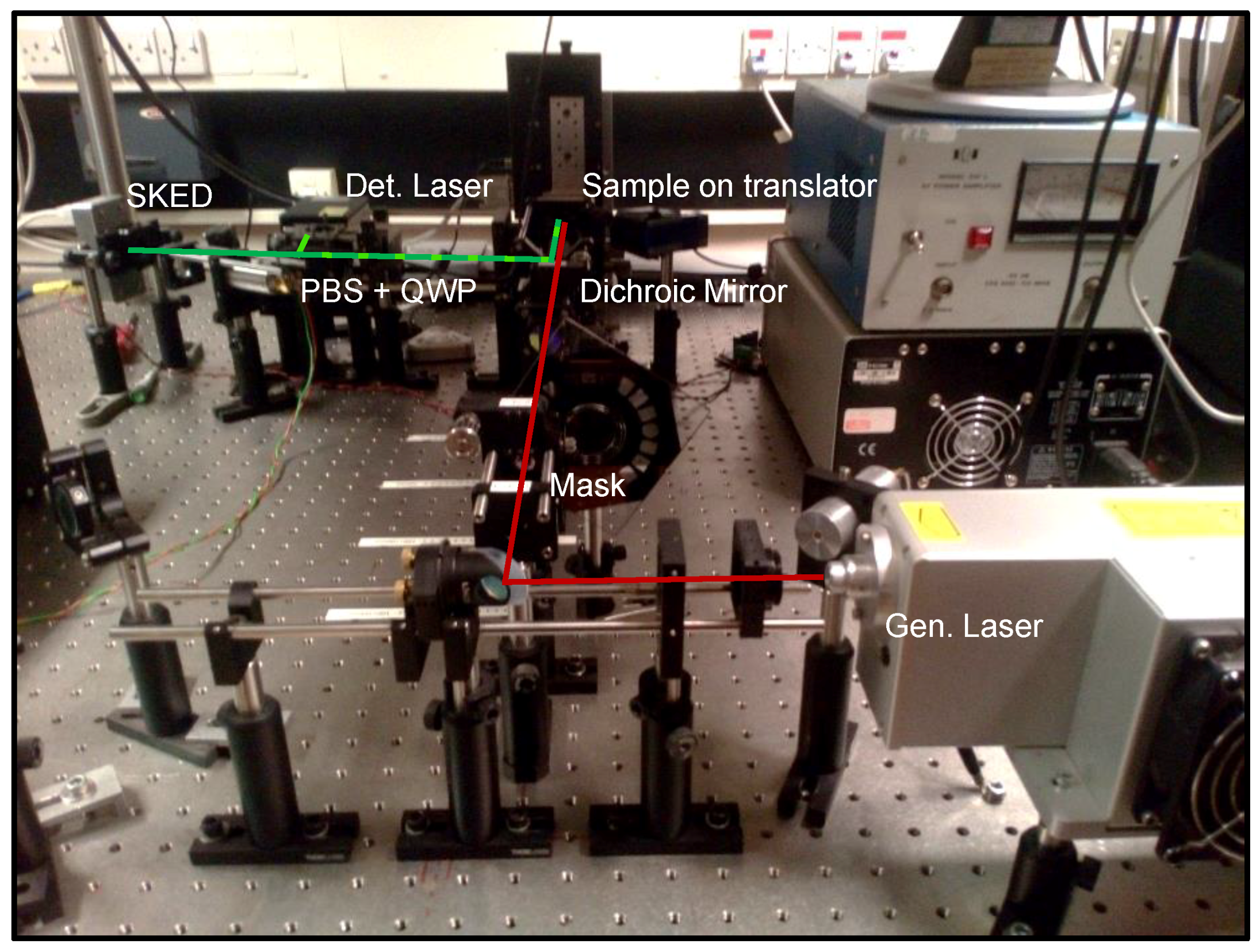
2. Instruments and Methods

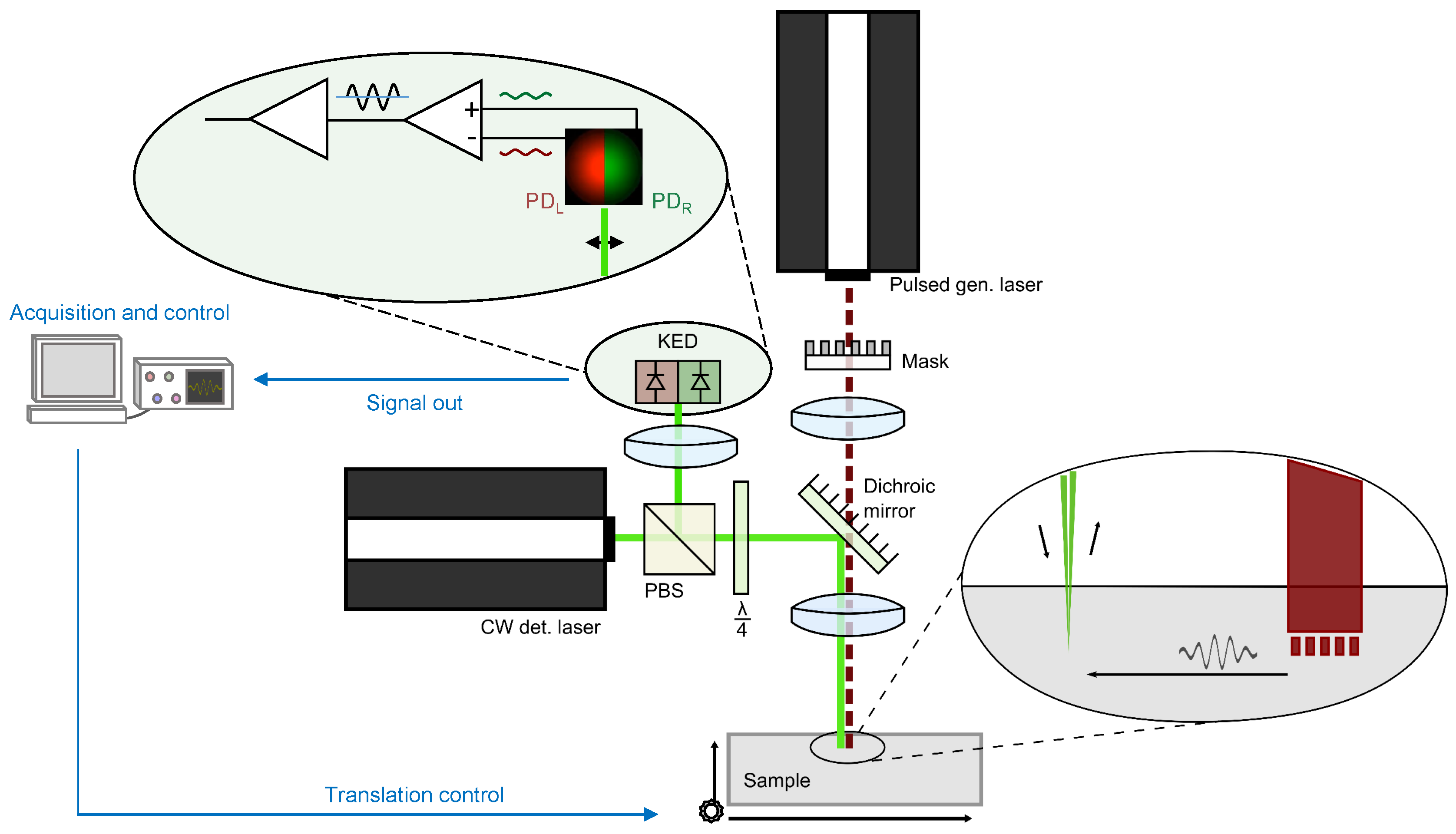
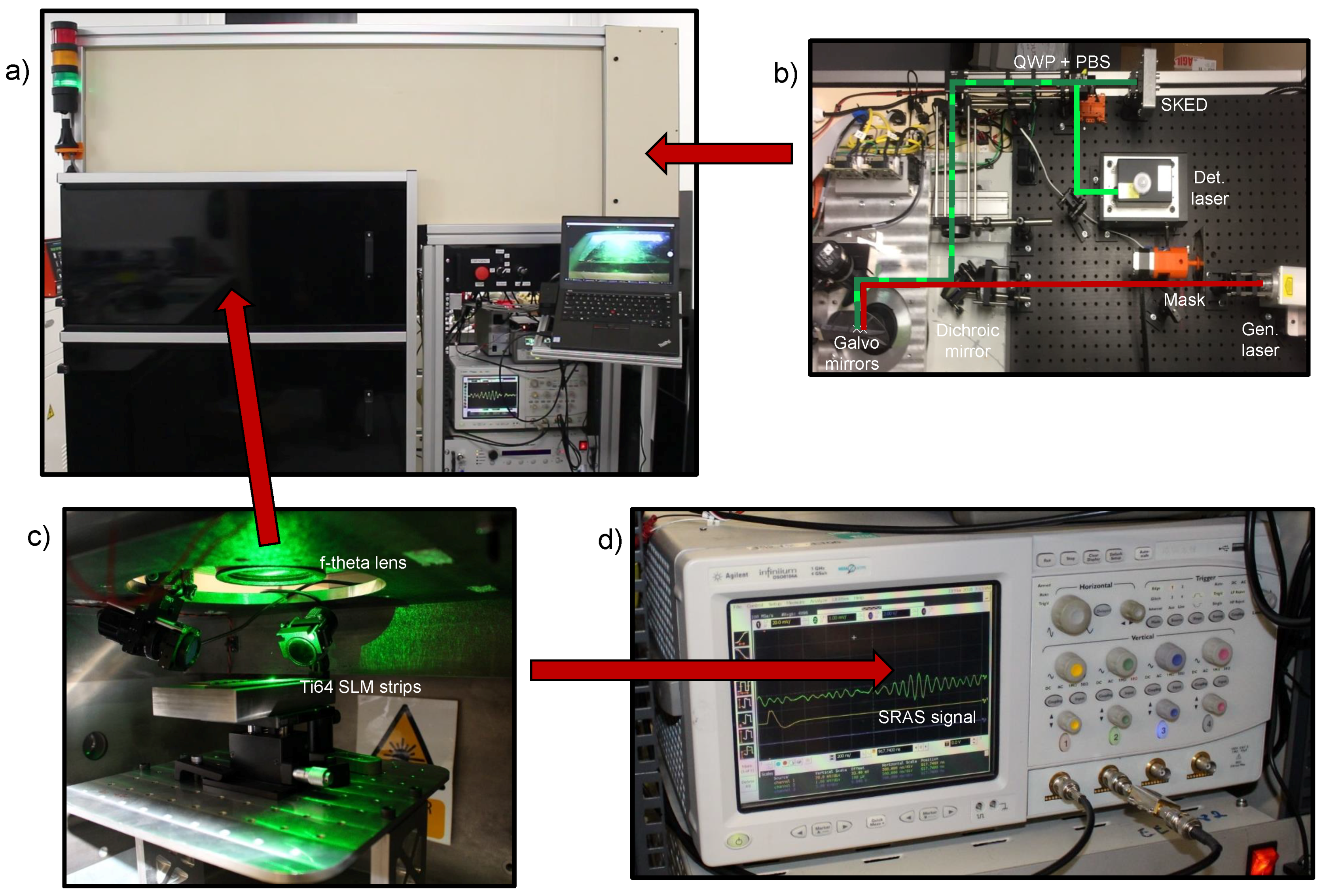
2.1. Spatially Resolved Acoustic Spectroscopy

SRAS is a laser ultrasound evaluation technique that can be used to measure a variety of material properties of a sample under inspection [8]. In brief, SRAS works by generating surface acoustic waves (SAWs) on samples using a pulsed laser. The perturbation on the surface due to the SAW is measured using another laser and a detector. Where SRAS differs from other laser ultrasound techniques is in the method of generating the surface wave—a periodic grating pattern is used to image lines of the incident pulsed laser. This creates a surface acoustic wave packet, where the frequency within the envelope is determined by the distance between the pulsed laser lines and the speed of the wave. Figure 1 shows a simplified SRAS schematic.
When used conventionally, the surface wave generated is a Rayleigh wave (air/solid interface with infinite half space) [11]—the wave packet generated in this regime is non-dispersive, and therefore the frequency ( f s ) within the packet remains constant from the point of generation. Given this occurrence, the surface wave velocity ( v s ) at the point of generation can be easily calculated using;
v s = f s λ g
where λ g is the distance (or period) between the incident pulsed laser lines, referred to as the grating wavelength. This points to one of the major strengths in using SRAS over conventional laser ultrasound techniques which measure wave velocity through time-of-flight. Detection of the waves can be made at any point along the wave propagation path, including adjacent to the generation point. This is useful for inspecting material in which heavy wave attenuation occurs. In addition to this, and considering that the measurement is made of the frequency rather than the amplitude, the influence to the measured signal is limited to the generation area, and not to material heterogeneity—this allows for strict control of the spatial resolution, without requiring multipoint measurements and post-process reconstruction. Rapid velocity measurements can be made using SRAS, with the reported systems in this paper used to raster scan samples.
The generated SAW (i.e., Rayleigh) velocity is dependent on the elastic properties of the material under inspection, which can change depending on factors such as sample composition, temperature and crystallographic orientation. Using SRAS, it is possible to image a material’s microstructure, by obtaining the material’s elastic constants (obtained through literature) and measuring the SAW phase velocities (by measuring SAW velocities in different directions), as all are related. Practically, the process of directly determining the orientation (the inverse problem) is difficult to solve, so a fitting algorithm is used instead [12]. The outcome of the implemented algorithm can be used to create inverse pole figures—there have been a number of past publications comparing obtained crystallographic grain orientation information using the SRAS technique against electron backscatter diffraction (EBSD) [13,14,15,16,17]. If the interrogation area is larger than the crystallographic grain size, then the predominant velocity in the area is measured—the material texture is imaged instead [9,10].
A SRAS system used to demonstrate the technique was first reported on in 2014 [18]. This system uses an IR (1064 nm) Q-switched pulsed laser (AOT-YAG-10Q, Advanced Optical Technology Ltd., Basildon, UK) to generate surface acoustic waves. In order to create the amplitude pattern that is incident on a sample, a mask made of quartz with a chrome coated grating is imaged on to the surface using the IR laser. The pulse duration of the IR laser is important as it defines the available bandwidth of the frequency within the generated SAW packet—in this setup, the pulse width of the laser is less than 2 ns. As SRAS is intended to be a non-destructive evaluation (NDE) technique, the system operates in the laser ultrasonic thermoelastic regime where waves are created in a solid sample by the sudden expansion due to localised heating—this is in contrast to the laser ultrasonic ablation regime where sufficient energy is applied such that the recoil the material experiences from the process of evaporation generates the ultrasound wave. The energy per pulse of the IR laser used in this setup is between 50–150 μ J at a repetition rate of 2 kHz. In the standard configuration, this system images eight lines with a period λ g = 24 μ m. A 200 mW green (532 nm) continuous wave (CW) laser (Laser Quantum Torus), focused down to Ø8 μ m, is used for detection. As a SAW approaches the point where the detection laser is incident, the perturbation of the surface slightly changes the angle of the returned beam.
In this setup, the reflected beam is measured using a knife edge detector (KED)—a detector based on measuring optical beam deflection (ODB) [19]. The KED contains a split photodiode, with the optical system designed such that the beam return is incident exactly between the split photodiode. The photocurrent generated is proportional to light intensity incident on each photodiode, and as the sample surface is perturbed (due to the SAW), a wave packet signal is generated off both photodiodes, opposite in phase. A differential amplifier circuit is then used to amplify the signal and remove common mode. A complete image of the SAW velocities are made by raster scanning the inspection sample using two high precision translation stages (M-531.DD, Physik Instrumente (PI) GmbH & Co. KG, Karlsruhe, Germany), which provides up to 300 mm of travel in two dimensions. The robustness of this system allows for single shot measurements to be made (i.e., no signal averaging required). A single direction SAW velocity is rapidly determined by performing a fast Fourier transform on the measured waveform, finding the maximum frequency response, and calculating the velocity using the associated frequency—the value of the frequency response is proportional to the measured signal power. Given the repetition rate of the IR laser, the scanning scheme implemented, and measurement overheads, the typical scan speeds are between 1000–1500 pts/s. To obtain the SAW phase velocities, the mask is rotated in order to propagate the generated surface waves in different directions—the detection laser also follows with the rotating pattern. Using the described generation and detection lasers, this setup has been used to image the microstructure of titanium, nickel, steel and aluminium based alloys [13,14,15,20], as well as non-metallic materials such as polycrystalline silicon samples (once a metallic coating is applied) [16].
One of the main restrictions of this system (but not of the technique in general) is that the inspection sample requires a smooth, mirror-like surface, or it must be prepared through polishing. With a smooth non-transparent surface, the beam profile of the detection laser is mostly preserved when reflected, in this case a singular Gaussian beam. To enable this specular reflection, the sample surface roughness should be less than the Rayleigh criterion [11].
Δ h < λ d 8 cos θ
where Δ h is the standard deviation of the surface roughness, λ d is the detection laser wavelength, and θ is the angle of incidence. In practice, a signal is obtainable using this system if the sample has the surface roughness R a < 100 nm.
With rough surfaces such as those seen on as-deposited SLM samples, the return beam becomes a diffuse reflection—instead of a Gaussian beam, speckles are incident on the split photodiode of the KED, with no detectable signal measured when deflection occurs (the combination of multiple speckles moving across both photodiodes outputs an almost zero average signal). This concept is illustrated in Figure 2a,b.
To measure an ultrasound signal on a rough surface, other detector schemes can be used. Adaptive interferometer techniques have been used to measured ultrasound on rough surfaces with some frequency restrictions [21,22], with developed confocal Fabry-Perot interferometer systems potentially being able to make ultrasound measurements limited only by the electronic circuit response [23,24]. A popular detection method of measuring high frequency ultrasound (up to 1 GHz) on rough surfaces consistently involves using two wave mixing (TWM) setup [25]. A photorefractive crystal is used to interfere the diffuse light return with a locally adapted reference beam, however, an amount adaption time is required before a measurement can be made, limiting scan speeds. Additionally, interferometric methods are often susceptible to microphonics and vibration. Other techniques that have been investigated include photodetector arrays with multiplexed laser interferometers [26] and quadrature demodulation for multi-speckle processing [27].

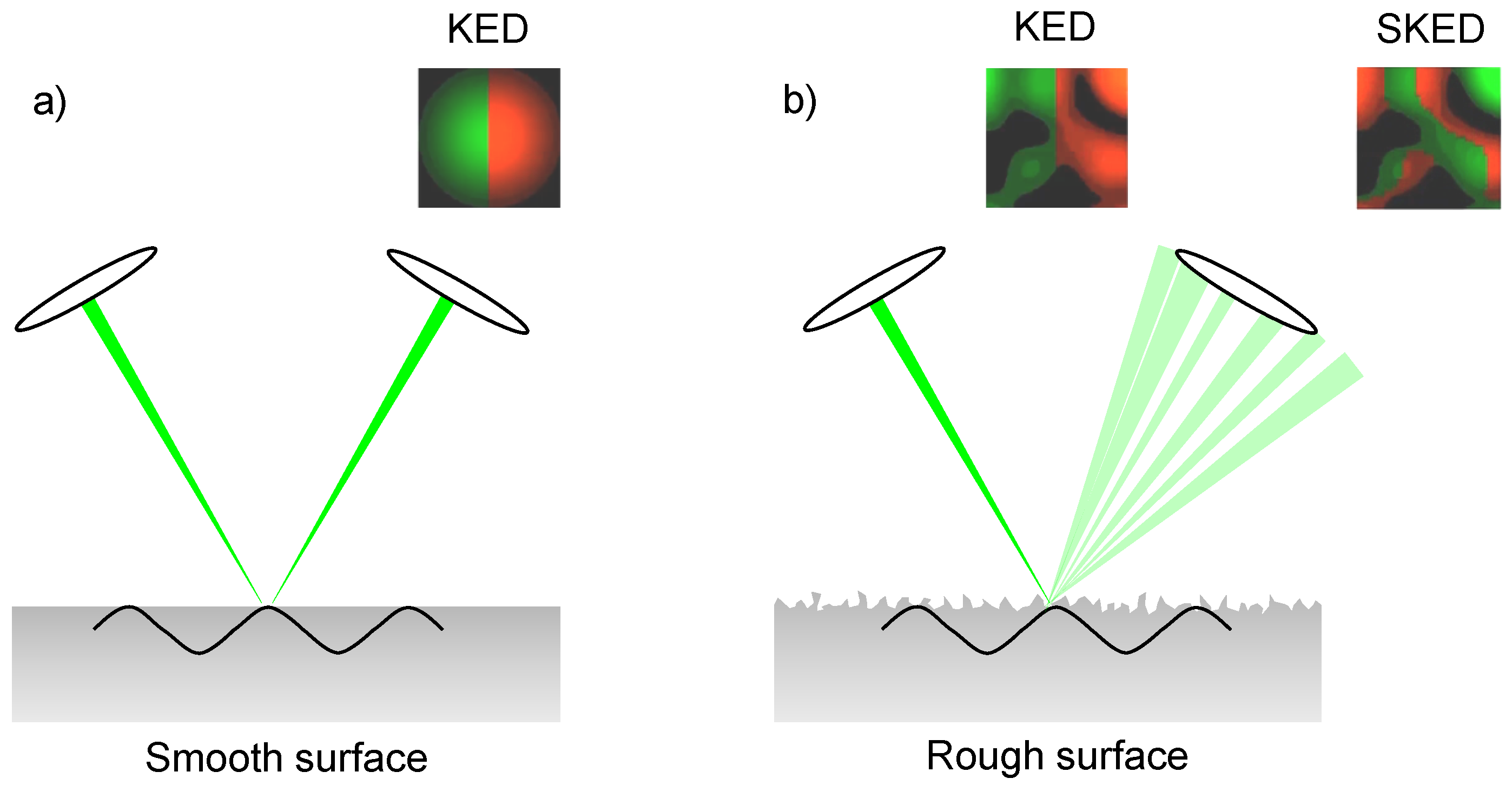
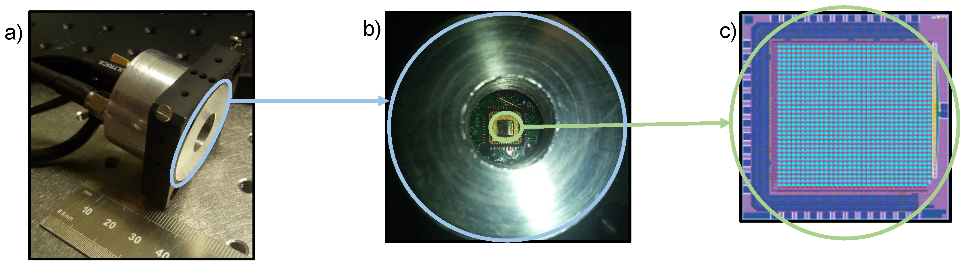
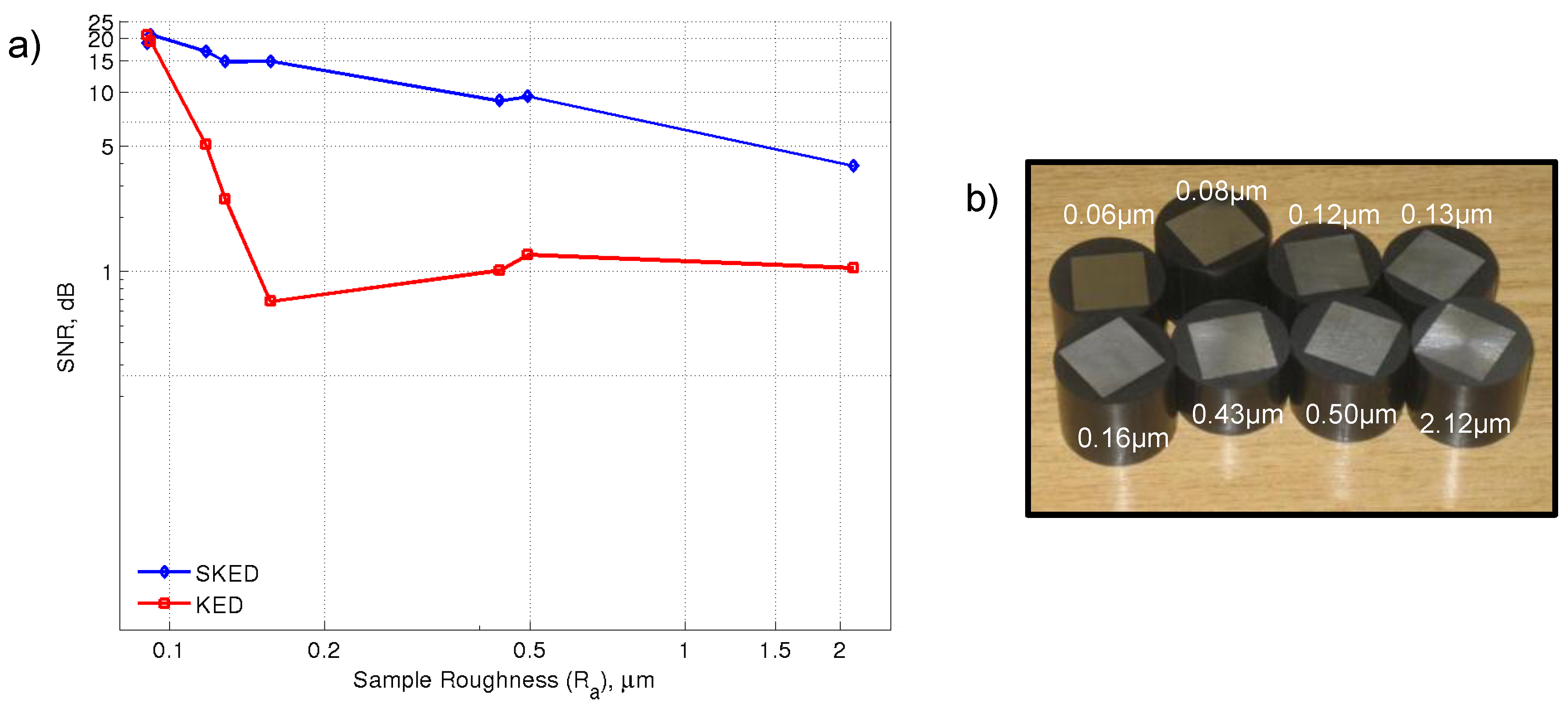
2.2. Speckle Knife Edge Detector
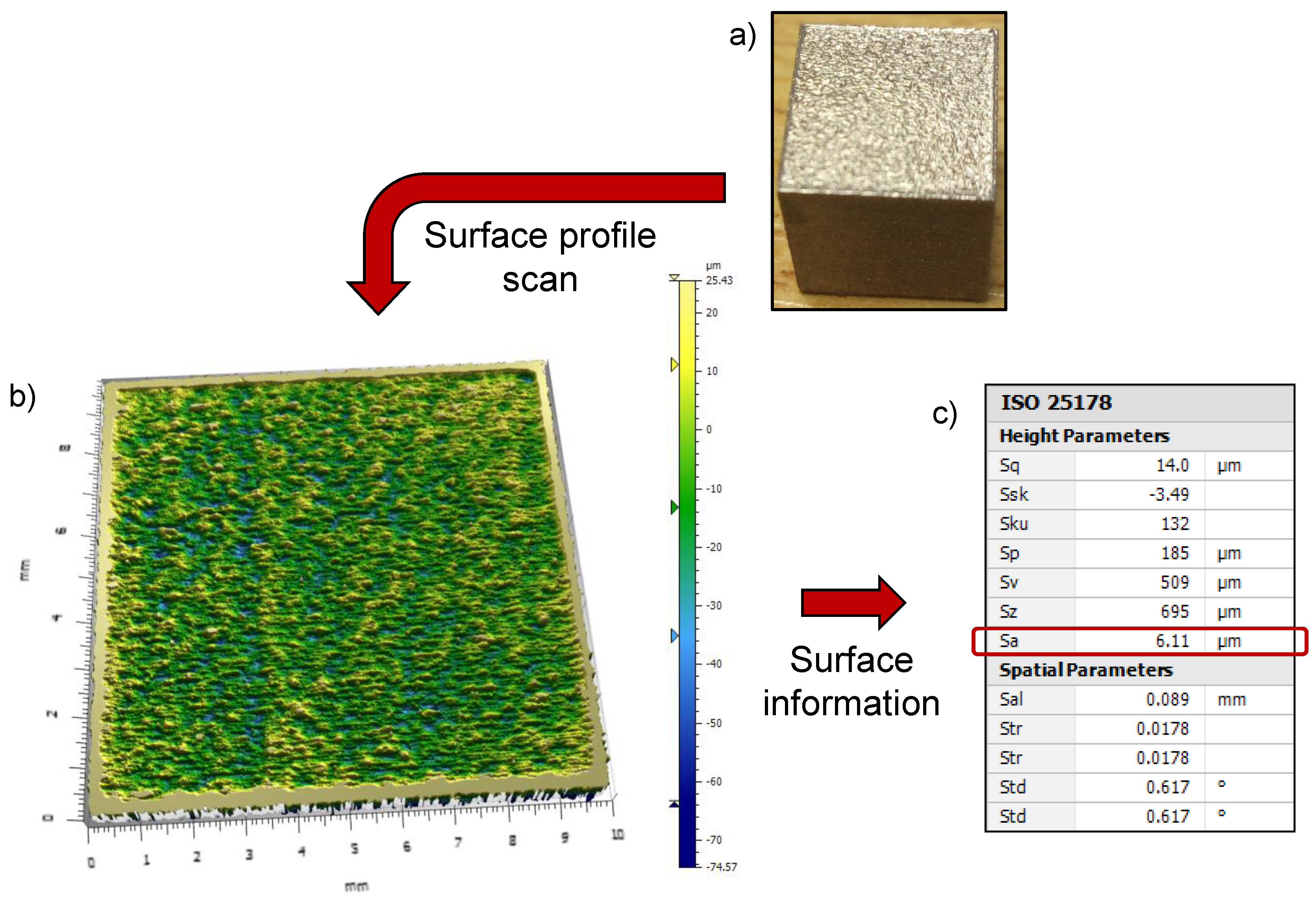
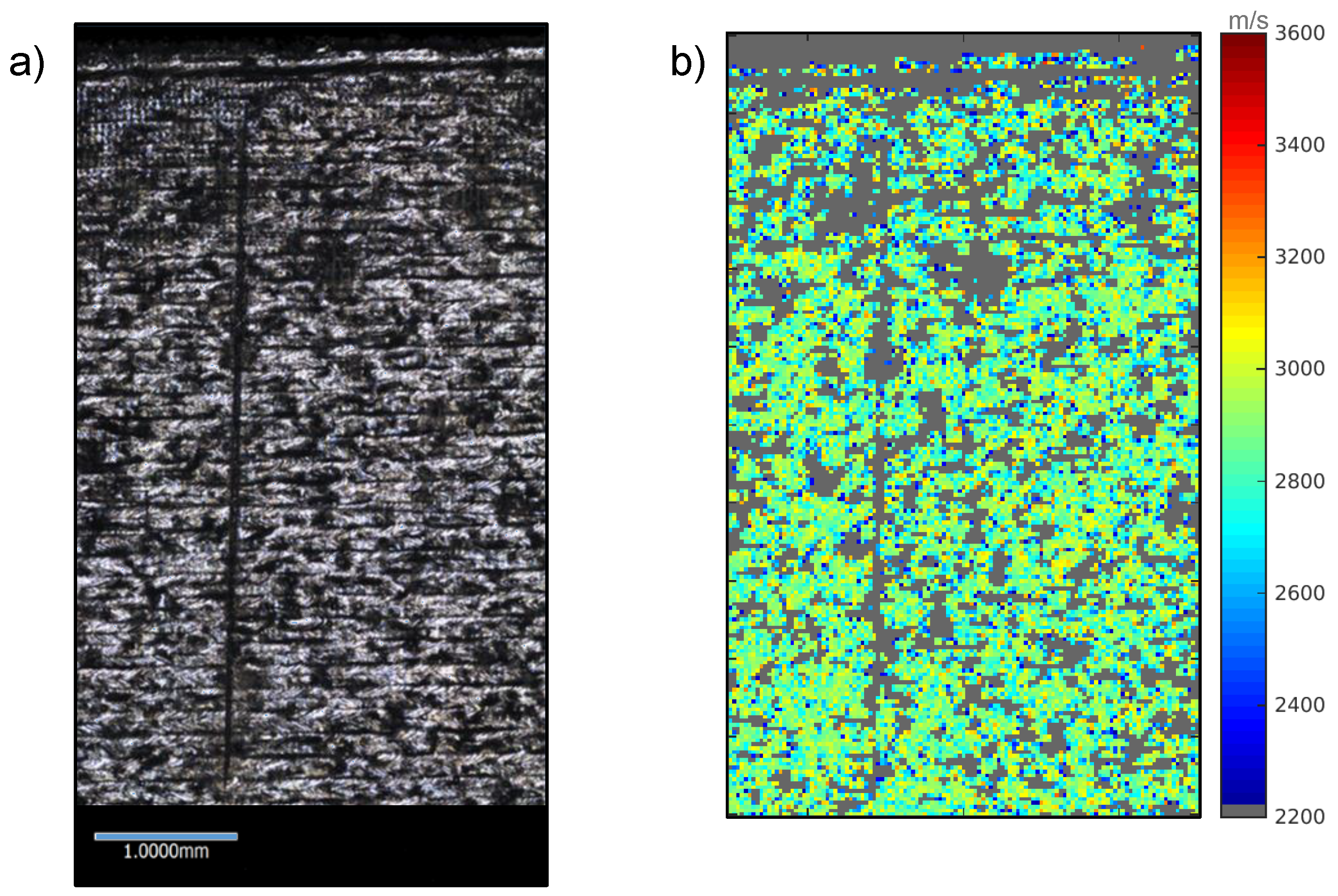
A previously reported detector developed by the authors, known as the speckle knife edge detector (SKED) [28,29], has been implemented as an all-electronic chip based device. As a concept, the SKED works as an expanded knife edge detector—in place of the two adjacent photodiodes there is an array of photodiodes. In the scenario where a speckle field is incident on the array, each speckle can be considered as an individual detection beam. Assuming that the size of each speckle is larger than two photodiodes, a knife edge `photodiode pair’ can be established, where each side of the `pair’ can contain the signal measured by multiple photodiodes. The signal obtained by measuring the deflection on all the incident speckles can be combined. An example speckle pattern split is shown in Figure 2b.
For the SKED concept to function, the output channel that each individual photodiode is connected to must be configurable. This process can be automated by observing the intensity gradient across a selection of pixels (usually a row or column) and grouping sets of pixels to the two different outputs based on when an intensity zero crossing occurs, i.e., when there is an apparent maximum or minimum in intensity, effectively splitting a speckle. As the SKED concept is classified as an OBD detector, it can still be considered robust in the presence of environmental vibration.
A number of custom SKED silicon chips had been developed based on this concept. The latest iteration was fabricated using a 0.35 μ m CMOS process—a 32 × 32 pixel array with 62 μ m pitch and 27% photosensitive area. Simulations of the chip show that the time required to switch between a configuration state and signal output is less than 0.5 μ s (equivalent to speckle adaption time), meaning theoretically 1 MSamp/s is possible. The simulated 3 dB bandwidth is 46 MHz when half the pixels are connected to the outputs (the bandwidth of the SKED increases as the number of pixels connected to the output decreases). To interface with the SKED chip, PCBs have been designed to output the detected ultrasound signal and to control the chip through USB via a PIC microcontroller—the most recent version is contained within a Ø 31.5 mm metal tube, which allows for a SKED device to be mounted inside an optical 35 mm cage plate holder (as shown in Figure 3a,b).
To enable measuring on rough surfaces, a free-space benchtop SRAS setup was designed and built. A photograph of the setup is shown in Figure 4. Aside from the detection aspect, the other major consideration is the propagation of ultrasound on the rough surface. The attenuation of the wave is a complicated problem, as it is dependent on the surface wave frequency and the characteristics of the rough surface—the attenuation rate along a determined length is proportional to the fifth power of the frequency of the Rayleigh wave given that the wavelength of the Rayleigh wave is longer than the transverse correlation length of the surface roughness [30,31,32]. One of the key advantages of using SRAS is that the surface wave can be detected adjacent to the wave generation area—this is in contrast to other laser ultrasound techniques that measure time-of-flight and require a suitable distance between generation and detection for accuracy. The rough surface SRAS setup was designed so that the mask wavelength ( λ g ), and therefore frequency ( f s ), can be easily changed. Considering that the definition of the measured frequency is controlled by the number of fringes incident on the sample (e.g., 8 lines), fixing the number of lines and increasing the mask wavelength (i.e., creating a larger interrogation area) would decrease the spatial resolution of a resultant acoustic velocity image map, but would ensure a sufficiently large amplitude wave would propagate to the detection point.
Similar to the smooth surface SRAS setup, this rough surface setup uses an IR (1064 nm) Q-switched laser (FQ-800-5-Y-1064, Elforlight Ltd., Daventry, UK) as the SAW generation source, providing ∼600 μ J per pulse, over a period of 8 ns with a repetition rate of 1 kHz—a chrome grating mask is imaged using this laser. A 1.5 W green (532 nm) CW laser (Samba 05-01, Cobolt AB, Solna, Sweden) is used as the detection laser. A 50.8 mm, f = 100 mm collection lens is used to capture part of the diffuse reflection, which is imaged onto the SKED device.
It can be difficult to completely quantify the improvement of using the SKED over the KED as a detector for measuring on rough surfaces, as factors that include (but are not limited to) the sample surface topology, peak-trough frequency and gradients, material reflectivity, and optical arrangement and alignment. As demonstrations, two simple experiments were conducted to illustrate the rough surface SRAS capability of the SKED.
The first experiment conducted shows the retention in signal-to-noise as surface roughness is increased on a similar sample—eight blocks of aluminium were prepared using a variety of polishing and grinding techniques. The roughness ( R a ) of each sample was measured using an AFM (Figure 5b). A SRAS scan was conducted on all samples ( λ g = 300 μ m) using both the SKED and KED in the same setup—the average measured SNR on all samples is shown in Figure 5a. In this test case, the SNR when using the KED as the ultrasound detector decreases dramatically as the sample roughness approaches R a 150 nm—the average SNR fluctuates around 1 dB due to the surface profile randomness. The measurement SNR when using the SKED also decreases (due to the decrease in incident optical intensity on the sensor), but at a much lower rate—a signal was still observable on the sample with surface roughness R a 2 μ m.
The second experiment conducted was to illustrate that the SKED can be used to measure the microstructure of samples, even in the presence of roughness (as long as λ g R a ). A large grain Ti-6Al-2Sn-4Zr-6Mo (Ti6246) block was polished to a surface finish of R a 100 nm, with the bottom-left corner of the block reground to a surface finish of R a 600 nm. The wavelength used for this experiment was λ g = 150 μ m. Figure 6a shows a photograph of the sample, Figure 6b,c shows output velocity image from the SRAS setup (i.e., SAW velocity at each point in one direction) using the KED and SKED as detectors, respectively. Figure 6d,e shows the maximum frequency response at each measurement point from the SRAS scans when the KED and SKED were used as detectors, respectively.
As seen in both the KED and SKED velocity images, the sample microstructural contrast is observable in the smooth surface region. It can be seen that the surface topology in the smooth region is not consistent, i.e., there are sections that contain machining marks or scratches—this can be seen as a reduction in the amplitude in the KED measured signal (Figure 6d)). No signal is observable in the rough surface region using the KED (the velocity plotted is of the random noise in the system, usually this is filtered out). When the SKED is used as the detector, the microstructure contrast is clearly visible in the rough surface region (Figure 6c). The drop in the SKED frequency response in the rough region is consistent with the findings from the first experiment.

3. Results

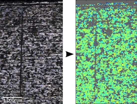
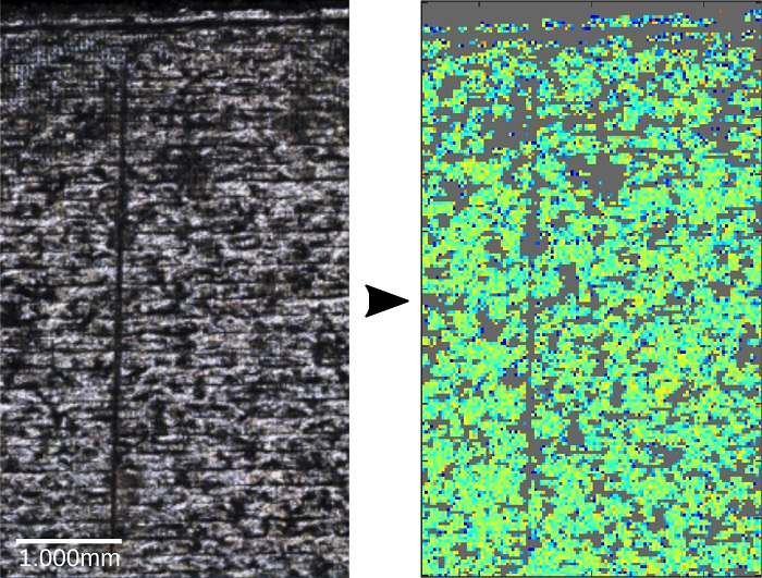
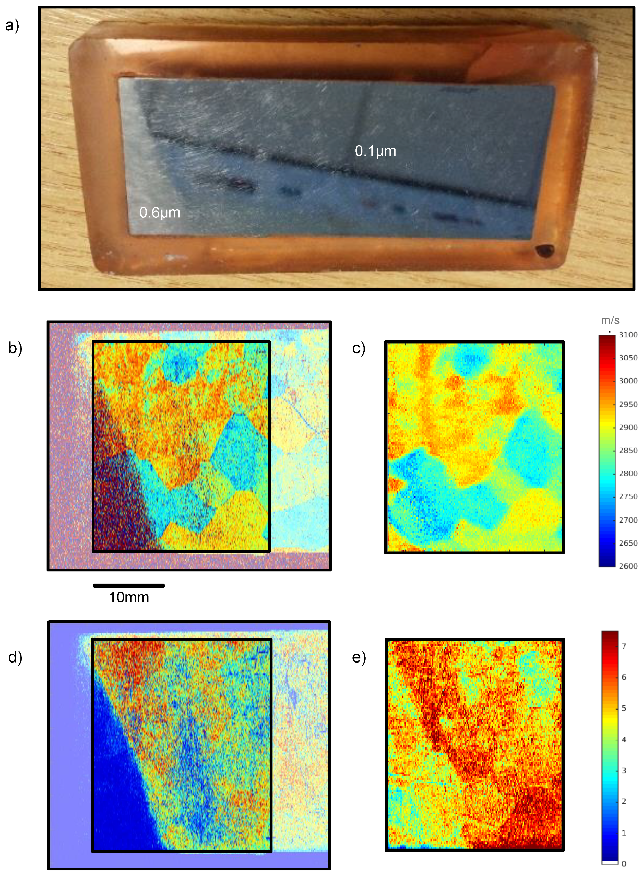
3.1. SAW Velocity Images on As-Deposited SLM Samples

In order to realise an in-situ additive manufacturing inspection system, the technique must be able to operate on the rough surfaces produced by the stochastic manufacturing process. The additive manufacturing process considered for this study was selective laser melting (SLM)—using commercially available SLM machines, the flatness of parts in the macro zone can be well controlled (i.e., topology), with the micro level roughness of the part defined by various built parameters such as powder size, material, build pattern regime, and applied energy [6].
A 10 × 10 × 10 mm 3 cube was built using Ti64 powder feedstock (powder size: ∼30 μ m) on a Renishaw AM250 machine. The sample was made using a meander– 90 hatching pattern, with the laser build power set to 110 W.
As stated, the finished-part surface roughness is dependent on a number of machine and environmental factors—the same is also true for part-built components, a consideration for inspecting in-situ. A reasonable assumption would be that the finished-part surface roughness would be comparable with the inter-layer profile, given unchanging and controlled build parameters.
The surface profile of the built part was measured using a focus variation microscope (Alicona InfiniteFocus)—a reconstruction of the sample surface profile is shown in Figure 7b, with the surface profile measurements made by this instrument shown in Figure 7c. The S a parameter, an areal roughness measurement (mean height deviation of a surface area), of the centre area is highlighted in the figure—this is roughly S a 6 μ m.
Before performing a SRAS scan on the sample, a line was scored into the surface to provide an identifying mark and was then optically imaged using a microscope, shown in Figure 8a. A small area SRAS scan (3 mm × 5 mm) was conducted with 25 μ m steps along both the x and y axes using a λ g = 250 μ m pattern, producing a frequency f s 12 MHz. The produced SRAS velocity image is shown in Figure 8b. The image shows the variation in the texture across the sample, with the velocity plotted within the expected range for Ti64. This velocity map is consistent with other Ti64 samples produced in a previous publication [10], as well as SLM Ti64 texture images seen in literature [33,34]. The images also show areas of low signal amplitude as a grey colour. This could be due to a low light return due to a large surface height variation—these features are seen in the optical micrograph. Additionally, this could indicate the presence of subsurface pores or cracks which do not allow SAW propagation [9].

3.2. Integrating a SRAS System inside a SLM Build Chamber

The optical bench-top system shows that a rough-surface SRAS system is possible. However, an engineering challenge exists in implementing a SRAS setup inside an additive manufacturing build environment, specifically a SLM build chamber, if the aim is to demonstrate the potential of an in-situ inspection system.
To enable this investigation, a barebone SLM shell was acquired from Renishaw (AM250, Renishaw plc., Stone, UK). The rough-surface SRAS setup was modified, incorporating two galvanometer 50 mm mirrors (O-QS30A50D40B24001, Nutfield Technology, Hudson, NH, USA) and a f = 100 mm f-theta lens, to provide translation and to collect a large amount of the reflected speckle (which is then imaged onto the SKED), shown in Figure 9a,b. This optical arrangement is commonly seen in SLM machines for translating the build laser—the integrated SRAS system was intentionally designed to provide compatibility with the SLM design, strengthening the case for a `SRAS AM add-on tool’.
As this work is in progress, the optical arrangement requires further optimisation. A scan of Ti64 strips, built with parameters similar to the sample in the previous section, reveals that SRAS signals can be seen only at certain locations on the sample (shown in Figure 9c,d). This is due to topographical changes on the sample, where there were not enough light returns through the f-theta lens to make a measurement. Plans for improving the integrated SRAS setup include changing the beam profile of the detection laser, where incident energy density is maintained but power is increased, increasing the repetition rate of the generation laser whilst proportionally increasing signal averaging, and implementing a multi-point detection system around the build chamber.

4. Discussion

An active field of study is the investigation of inspecting additive manufactured parts. One of the features of this current manufacturing process is the method of build, where shaped material is added, often in layers—this makes the process available for surface-based inspection on the bulk material if measurements are conducted in-process.
Very few non-destructive evaluation techniques are suited to taking rapid measurements of defects inside an AM build environment. These defects include newly created subsurface voids created by keyholing effects—sizing and locating the features could become important when considering defect density rather than singular defects.
This paper introduces a SRAS system capable of detecting surface ultrasound waves on the rough-surface of an as-deposited SLM sample. The system is an all-optical implementation, which does not require instrument contact for measurement and is capable of detecting subsurface defects [10]. The primary market for AM tool manufacturing is the high-value sector (e.g., aerospace), where microstructure information for high-performance is required by the end user. The described inspection system is also capable of imaging material texture on an as-deposited sample.
The work presented in this paper, comprising the rough-surface SRAS setup and the SLM chamber integrated SRAS system, illustrates the potential that this system has in performing in-situ part defect and material characterisation. For a practical implementation, there are a number of challenges to overcome. A raster scanning strategy is employed, where it is possible to collect single-shot SRAS waveform measurements (roughly 1500 points per second) [18]. This is a slower measurement capture time when compared to inspection systems based on camera arrays (e.g., thermography, metrology). Additionally, limitations of this optical arrangement exist where the light intensity incident on the detector is greatly reduced due to the diffuse reflection. A number of averages is required to improve SNR, further increasing scan times. The spatial resolution of the optical and acoustic images can be defined using the detection beam size and generation patch size on the surface, respectively—providing a singular answer for the size and depths of subsurface defects becomes a challenge [35]. Lamb wave ultrasound inspection of single crystal materials has been investigated by the authors [36,37], with recent work published on imaging defects in carbon-fibre reinforced plastic materials [38]—for use in additive manufacturing, the anisotropy of the material will determine whether a subsurface pore can be distinguished. If a material is isotropic, detecting defects close to the surface (within 2 λ g ) should be as resolvable as the material microstructure, with deeper defects having a lesser effect on the velocity measured.

Author Contributions

Conceptualisation, R.L. and S.S.; Methodology, R.P., M.H. and S.A.-Y.; Software, R.P., M.H., P.D., S.A.-Y., R.L., S.S. and M.C.; Validation, R.P.; Investigation, R.P., P.D., D.P. and S.A.-Y.; Resources, M.H.; Data Curation, R.P. and S.A.-Y.; Writing—Original Draft Preparation, R.P.; Writing—Review & Editing, R.P., P.D., R.S., R.L., S.S., A.C. and M.C.; Supervision, R.S., S.S., A.C. and M.C.; Funding Acquisition, S.S. and A.C.

Funding

This work was supported by the Engineering and Physical Sciences Research Council [grant number EP/L022125/1] through the `UK Research Centre in Nondestructive Evaluation’.

Acknowledgments

The authors would like to thank Nick Jones (Renishaw plc) for providing the SLM build chamber for our integration work. The authors would also like to acknowledge Alex Jackson-Crisp (University of Nottingham) for his assistance with constructing enclosures.

Conflicts of Interest

The authors declare no conflict of interest.

Abbreviations

The following abbreviations are used in this manuscript:
AFMAtomic force microscope
AMAdditive manufacturing
CWContinuous wave
IRInfra-red
NDENon-destructive evaluation
KEDKnife edge detector
ODBOptical beam deflection
PCBPrinted circuit board
SAWSurface acoustic wave
SKEDSpeckle knife edge detector
SLMSelective laser melting
SNRSignal-to-noise ratio
SRASSpatially resolved acoustic spectroscopy
TWMTwo-wave mixing
XCTX-ray computer tomography

References

  1. Gibson, I.; Rosen, D.W.; Stucker, B. Additive Manufacturing Technologies; Springer: Berlin/Humberger, Germany, 2010; ISBN 978-1493921126. [Google Scholar]
  2. Aboulkhair, N.T.; Everitt, N.M.; Ashcroft, I.; Tuck, C. Reducing Porosity in AlSi10Mg Parts Processed by Selective Laser Melting. Addit. Manuf. 2014, 1, 77–86. [Google Scholar] [CrossRef]
  3. Zhao, C.; Fezzaa, K.; Cunningham, R.W.; Wen, H.; De Carlo, F.; Chen, L.; Rollett, A.D.; Sun, T. Real-Time Monitoring of Laser Powder Bed Fusion Process Using High-Speed X-ray Imaging and Diffraction. Sci. Rep. 2017, 7, 3602. [Google Scholar] [CrossRef] [PubMed]
  4. Xu, Z.; Hyde, C.J.; Thompson, A.; Leach, R.K.; Maskery, I.; Tuck, C.; Clare, A.T. Staged Thermomechanical Testing of Nickel Superalloys Produced by Selective Laser Melting. Mater. Des. 2017, 133, 520–527. [Google Scholar] [CrossRef]
  5. Tammas-Williams, S.; Zhao, H.; Leonard, F.; Derguti, F.; Todd, I.; Prangnell, P.B. XCT Analysis of the Influence of Melt Strategies on Defect Population in Ti–6Al–4V Components Manufactured by Selective Electron Beam Melting. Mater. Charact. 2015, 102, 47–61. [Google Scholar] [CrossRef]
  6. Senin, N.; Thompson, A.; Leach, R.K. Characterisation of the Topography of Metal Additive Surface Features with Different Measurement Technologies. Meas. Sci. Technol. 2017, 28, 095003. [Google Scholar] [CrossRef]
  7. Raplee, J.; Plotkowski, A.; Kirka, M.M.; Dinwiddie, R.; Okello, A.; Dehoff, R.R.; Babu, S.S. Thermographic Microstructure Monitoring in Electron Beam Additive Manufacturing. Sci. Rep. 2017, 7, 43554. [Google Scholar] [CrossRef] [PubMed] [Green Version]
  8. Sharples, S.D.; Clark, M.; Somekh, M.G. Spatially Resolved Acoustic Spectroscopy for Fast Noncontact Imaging of Material Microstructure. Opt. Express 2006, 14, 10435. [Google Scholar] [CrossRef] [PubMed]
  9. Hirsch, M.; Catchpole-Smith, S.; Patel, R.; Marrow, P.; Li, We.; Tuck, C.; Sharples, S.D.; Clare, A.T. Meso-Scale Defect Evaluation of Selective Laser Melting Using Spatially Resolved Acoustic Spectroscopy. Proc. R. Soc. A Math. Phys. 2017, 473, 20170194. [Google Scholar] [CrossRef] [PubMed]
  10. Smith, R.J.; Hirsch, M.; Patel, R.; Li, W.; Clare, A.T.; Sharples, S.D. Spatially Resolved Acoustic Spectroscopy for Selective Laser Melting. J. Mater. Process. Technol. 2016, 236, 93–102. [Google Scholar] [CrossRef]
  11. Viktorov, I.A. Rayleigh and Lamb Waves: Physical Theory and Applications; Plenum Press: New York, NY, USA, 1970. [Google Scholar]
  12. Li, W.; Sharples, S.D.; Smith, R.J.; Clark, M.; Somekh, M.G. Determination of Crystallographic Orientation of Large Grain Metals with Surface Acoustic Waves. J. Acoust. Soc. Am. 2012, 132, 738–745. [Google Scholar] [CrossRef] [PubMed]
  13. Mark, A.F.; Li, W.; Sharples, S.; Withers, P.J. Comparison of Grain to Grain Orientation and Stiffness Mapping by Spatially Resolved Acoustic Spectroscopy and EBSD. J. Microsc. 2017, 267, 89–97. [Google Scholar] [CrossRef] [PubMed]
  14. Xiao, B.; O’Leary, R.; Gachagan, A.; Li, W.; Burnett, T. Accurate Finite Element Model of Equiaxed-Grain Engineering Material for Ultrasonic Inspection. In Proceedings of the IEEE 2014 International Ultrasonics Symposium 2014, Chicago, IL, USA, 3–6 September 2014; pp. 1364–1367. [Google Scholar] [CrossRef]
  15. Li, W.; Coulson, J.; Aveson, J.W.; Smith, R.J.; Clark, M.; Somekh, M.G.; Sharples, S.D. Orientation Characterisation of Aerospace Materials by Spatially Resolved Acoustic Spectroscopy. J. Phys. Conf. Ser. 2014, 520, 012017. [Google Scholar] [CrossRef] [Green Version]
  16. Patel, R.; Li, W.; Smith, R.J.; Sharples, S.D.; Clark, M. Orientation Imaging of Macro-Sized Polysilicon Grains on Wafers Using Spatially Resolved Acoustic Spectroscopy. Scr. Mater. 2017, 140, 67–70. [Google Scholar] [CrossRef]
  17. Speidel, A.; Su, R.; Mitchell-Smith, J.; Dryburgh, P.; Bisterov, I.; Pieris, D.; Li, W.; Patel, R.; Clark, M.; Clare, A.T. Crystallographic Texture Can Be Rapidly Determined by Electrochemical Surface Analytics. Acta Mater. 2018, 159, 89–101. [Google Scholar] [CrossRef]
  18. Smith, R.J.; Li, W.; Coulson, J.; Clark, M.; Somekh, M.G.; Sharples, S.D. Spatially Resolved Acoustic Spectroscopy for Rapid Imaging of Material Microstructure and Grain Orientation. Meas. Sci. Technol. 2014, 10, 25. [Google Scholar] [CrossRef]
  19. Scruby, C.B.; Drain, L.E. Laser Ultrasonics: Techniques and Applications; CRC Press: Boca Raton, FL, USA, 1990; ISBN 978-1845697358. [Google Scholar]
  20. Sharpies, S.D.; Li, W.; Clark, M.; Somekh, M.G. Microstructure Imaging Using Frequency Spectrum Spatially Resolved Acoustic Spectroscopy (F-SRAS). AIP Conf. Proc. 2010, 1211, 279. [Google Scholar] [CrossRef]
  21. Dewhurst, R.J.; Shan, Q. Optical Remote Measurement of Ultrasound. Meas. Sci. Technol. 1999, 10, 139–168. [Google Scholar] [CrossRef]
  22. Nakano, H.; Matsuda, Y.; Shin, S.; Nagai, S. Optical Detection of Ultrasound on Rough Surfaces by a Phase-Conjugate Method. Ultrasonics 1995, 33, 261–264. [Google Scholar] [CrossRef]
  23. Monchalin, J.P. Optical Detection of Ultrasound. IEEE Trans. Ultrason. Ferroelectr. Freq. Control 1986, 33, 485–499. [Google Scholar] [CrossRef] [PubMed]
  24. Blouin, A.; Padioleau, C.; Neron, C.; Levesque, D.; Monchalin, J.P. Differential Confocal Fabry-Perot for the Optical Detection of Ultrasound. AIP Conf. Proc. 2007, 894, 193–200. [Google Scholar] [CrossRef] [Green Version]
  25. Kamshilin, A.A. Adaptive Photorefractive Interferometers for Ultrasound Detection. Proc. SPIE 2002, 4919, 11. [Google Scholar] [CrossRef]
  26. Murray, T.W. Multiplexed Interferometer for Ultrasonic Imaging Applications. Opt. Eng. 2001, 40, 1321. [Google Scholar] [CrossRef]
  27. Pouet, B. Robust Laser-Ultrasonic Interferometer Based on Random Quadrature Demodulation. AIP Conf. Proc. 2006, 820, 233–239. [Google Scholar] [CrossRef]
  28. Sharples, S.D.; Light, R.A.; Achamfuo-Yeboah, S.O.; Clark, M.; Somekh, M.G. The SKED: Speckle Knife Edge Detector. J. Phys. Conf. Ser. 2014, 520, 012004. [Google Scholar] [CrossRef]
  29. Achamfuo-Yeboah, S.O.; Light, R.A.; Sharpies, S.D. Optical Detection of Ultrasound from Optically Rough Surfaces Using a Custom CMOS Sensor. J. Phys. Conf. Ser. 2015, 581, 012009. [Google Scholar] [CrossRef]
  30. Maradudin, A.A.; Mills, D.L. Attenuation of Rayleigh Surface Waves by Surface Roughness. Appl. Phys. Lett. 1976, 28, 573–575. [Google Scholar] [CrossRef]
  31. Eguiluz, A.G.; Maradudin, A.A. Frequency Shift and Attenuation Length of a Rayleigh Wave Due to Surface Roughness. Phys. Rev. B 1983, 28, 728–747. [Google Scholar] [CrossRef]
  32. Kosachev, V.V.; Lokhov, Y.N.; Chukov, V.N. Theory of Attenuation of Rayleigh Surface Acoustic Waves on a Free Randomly Rough Surface of a Solid. Zh. Eksp. Teor. Fiz. 1988, 94, 172. [Google Scholar]
  33. Simonelli, M.; Tse, Y.Y.; Tuck, C. Microstructure of Ti-6Al-4V Produced by Selective Laser Melting. J. Phys. Conf. Ser. 2012, 371, 012084. [Google Scholar] [CrossRef]
  34. Qiu, C.; Adkins, N.J.E.; Attallah, M.M. Microstructure and Tensile Properties of Selectively Laser-Melted and of HIPed Laser-Melted Ti–6Al–4V. Mater. Sci. Eng. A 2013, 578, 230–239. [Google Scholar] [CrossRef]
  35. Hirsch, M.; Patel, R.; Li, W.; Guan, G.; Leach, R.K.; Sharples, S.D.; Clare, A.T. Assessing the Capability of In-situ Nondestructive Analysis During Layer Based Additive Manufacture. Addit. Manuf. 2017, 13, 135–142. [Google Scholar] [CrossRef]
  36. Clark, M.; Linnane, F.; Sharples, S.D.; Somekh, M.G. Frequency Control in Laser Ultrasound with Computer Generated Holography. Appl. Phys. Lett. 1998, 72, 1963–1965. [Google Scholar] [CrossRef]
  37. Hong, Y.; Sharples, S.D.; Clark, M.; Somekh, M.G. Rapid Measurement of Surface Acoustic Wave Velocity on Single Crystals Using an All-Optical Adaptive Scanning Acoustic Microscope. Appl. Phys. Lett. 2003, 83, 3260–3262. [Google Scholar] [CrossRef]
  38. Maio, L.; Ricci, F.; Memmolo, V.; Monaco, E.; Boffa, N.D. Application of Laser Doppler Vibrometry for Ultrasonic Velocity Assessment in a Composite Panel with Defect. Compos. Struct. 2018, 184, 1030–1039. [Google Scholar] [CrossRef]
Figure 1. Schematic of a spatially resolved acoustic spectroscopy (SRAS) system capable of rapidly imaging surface acoustic wave (SAW) velocities on smooth flat surfaces. A grating pattern is imaged onto a sample using a pulsed IR beam, which generates a non-dispersive surface wave packet. The packet contains a frequency ( f s ) controlled by the period of the incident pattern ( λ g ) and the velocity of the surface wave at the point of generation ( v s )—the velocity is affected by surface grain orientation or defects. The generated wave perturbs a detection beam which is detected by the knife edge detector—the two out-of-phase intensity signals are passed through a differential amplifier and captured using a fast acquisition board or oscilloscope and PC.
Applsci 08 01991 g001
Figure 2. An illustrative laser ultrasound detection outline on a (a) smooth, (b) rough surface. On a smooth surface (a), the small deflection of a singular return beam can be measured using a knife edge detector, however, on a rough surface (b), the change in intensity seen on either photodiode due to the deflection of the speckle field is not detectable. The speckle knife edge detector (SKED) `splits’ the incident speckles into left/right channels across its detector array, allowing it to detect the small deflections in the speckle field.
Applsci 08 01991 g002
Figure 3. Photographs (a) and (b) show the current implementation of the SKED device inside a 35 mm cage plate holder. The length of the device is roughly 30 mm. The render (c) of the SKED chip shows the array of 32 × 32 active circuit photodetectors.
Applsci 08 01991 g003
Figure 4. A photograph of the rough-surface SRAS setup showing key component and the laser beam paths. The reflected speckles are captured through a large 50.8 mm lens, with the pattern imaged onto the SKED chip array. Precise control of the detection beam focus is required to ensure the speckles appear larger than two photodetectors on the SKED—this is confirmed by using observing configuration pattern of the SKED device via a USB output.
Applsci 08 01991 g004
Figure 5. (a) Graph showing the signal to noise of a 10 MHz ultrasound wave detected using the knife edge detector and SKED. Measurements were taken on each of the samples shown in (b). The mean signal of 707 points on each sample were used to calculate the SNR. The signal decreases rapidly between 100 nm < R a < 200 nm when using the KED to detect, whereas the signal is still observable at R a 2 μ m.
Applsci 08 01991 g005
Figure 6. A large grain Ti6246 block (a) was scanned using both the smooth surface SRAS setup and rough surface SRAS setup. The values shown in (a) indicates the roughness (in R a ) in that area of the sample. The measured SAW velocity (m/s) of the sample is shown in (b) using the smooth surface setup (c) using the rough surface setup. A box in (b) indicates the area of the sample that were scanned using both systems. Images (d,e) show the maximum signal amplitude (arb. units) detected using the smooth and rough surface setups respectively—both images show a decrease in response in the rougher region (which supports the findings from the previous experiment), however, a measurable signal is still observable when using the rough surface setup in the rough region.
Applsci 08 01991 g006
Figure 7. (a) Photograph of the Ti64 selective laser melting (SLM) sample under inspection, (b) a surface profile map of the SLM sample measured using the focus variation microscope, (c) height parameters measured using the microscope, which includes the highlighted S a value (∼6 μ m).
Applsci 08 01991 g007
Figure 8. (a) Optical micrograph of the Ti64 SLM sample (b) SRAS velocity map of a 3 mm × 5 mm area on the Ti64 SLM sample. The sample was scanned using a step size of 25 μ m in both directions, therefore the image produced is oversampled. In areas where a low or no signal is measured, it is coloured grey. Similar features can be seen in both images, which includes surface cavities and the line mark.
Applsci 08 01991 g008
Figure 9. Photographs of the SLM-integrated SRAS system, (a) fully enclosed (class 1 laser safe), (b) plan view of the SRAS setup, with components and beam path indicated, (c) a Ti64 SLM strip under inspection on a large build plate, (d) the signal obtained on the SLM sample on an oscilloscope. Aluminium plates, rubber seals and interlocks were designed into the enclosure as this SLM-SRAS chamber is intended to be a demonstration unit. The optical setup was positioned in a similar area to the actual SLM machine’s optics train. New software had been written to control acquisition and translation. The optics seen in the build chamber (c) were used to monitor the incident light and are not required to perform the SRAS inspection.
Applsci 08 01991 g009

