Improving the Gate-Induced Drain Leakage and On-State Current of Fin-Like Thin Film Transistors with a Wide Drain

1
Department of Electronic Engineering, National Taipei University of Technology, Taipei 106, Taiwan
2
National Nano Device Laboratories, Hsinchu 30078, Taiwan
*
Author to whom correspondence should be addressed.
Appl. Sci. 2018, 8(8), 1406; https://0-doi-org.brum.beds.ac.uk/10.3390/app8081406
Submission received: 23 June 2018
/
Revised: 9 August 2018
/
Accepted: 15 August 2018
/
Published: 20 August 2018
(This article belongs to the Special Issue Selected Papers from the 2017 International Conference on Inventions)
Abstract
:Polycrystalline silicon (poly-Si) thin film transistors (TFT) with a tri-gate fin-like structure and wide drain were designed and simulated to improve gate-induced drain leakage (GIDL), ON-state current, and breakdown voltage. The GIDL of fin-like TFTs (FinTFTs) examined in this study was dominated by longitudinal band-to-band tunneling (L-BTBT). Extending the wide drain can effectively suppress the longitudinal electric field near the drain and improve L-BTBT GIDL and breakdown. In addition, a wider drain can lead to a large cross section in the current path and improve the ON-state current. FinTFTs with wide drain exhibit a low GIDL, a high ON-state current, and high breakdown voltage, while maintaining favorable gate controllability.
1. Introduction
Polycrystalline silicon (poly-Si) thin film transistors (TFTs) [1,2,3,4] and oxide semiconductor TFTs [5,6,7,8] are suitable for use in system-on-panels (SoP) or system-on-glass (SoG) displays because of their higher electron mobility compared with that of amorphous silicon (a-Si). The attraction of using poly-Si TFTs in displays lies in their ability to integrate peripheral functional components such as a controller, a high-voltage driver, and memory into the display panel. Improving the breakdown characteristics of poly-Si TFTs has become an important issue for realizing SoP. To improve these breakdown characteristics, methods such as lightly doped drain [9,10], offset drain [11,12], and semi-insulating field plate [13,14] were proposed. However, these methods increase the series resistances, and the ON-state current is sacrificed. A field-plate (FP) structure can increase the breakdown voltage, as well as the ON-state characteristics [15]. In this study, an FP was adopted to improve the breakdown characteristics without sacrificing the ON-state current.
The carrier mobility of poly-Si TFTs can be improved by scaling the channel length, which results in a decrease in the number of grain boundaries, i.e., an increase in the grain size in the active region [16]. However, the short channel effect is exacerbated as the channel length decreases. Three-dimensional (3-D) multi-gate structures, such as double-gate, tri-gate, and gate-all-around (GAA) structures, have been proposed to improve gate controllability and protect against the short-channel effects of nanoscale transistors [17,18,19,20,21,22,23,24]. Therefore, a tri-gate fin-like structure with a channel length (L) of 0.2 μm was employed in this study.
For a two-dimensional conventional planer structure, transverse band-to-band tunneling (T-BTBT) in the gate/drain overlap region is the dominant mechanism for gate-induced drain leakage (GIDL) in the OFF-state [25,26,27]. However, for a 3-D structure such as a fin-like TFT (FinTFT) with a narrow channel wire width, band overlap between the valence band of the body and the conduction band of the drain region enables substantial lateral band-to-band tunneling (L-BTBT) of electrons from the body to the drain in the OFF-state [28,29]. This indicates that the mechanism of GIDL is L-BTBT for a 3-D structure. Recently, some studies have focused on minimizing L-BTBT in 3-D structures [30,31,32,33,34].
A dual-metal gate-stack architecture for nanowire field-effect transistors (FETs) [30] or nanowire junctionless FETs [31] can lead to a reduction in the electric field at the channel–drain extension interface width, which reduces L-BTBT-induced GIDL. In addition, a nanowire junctionless-mode FET with a long extension (the length between the source/drain electrode and the gate edge) has a lower GIDL current than does a nanowire inversion mode FET owing to a low doping concentration at the drain and thus a broad tunneling width [32].
The effect of a gate sidewall spacer on GIDL was investigated by Sahay and Kumar [33]. A nanowire metal–oxide-–semiconductor FET with high-κ spacer-like HfO2 has a low OFF-state current because of the low-peak electric field at the channel–drain extension interface; the OFF-state current increases as the dielectric constant of the spacer is reduced [33].
Because the GIDL current largely depends on drain extension doping, the influence of the lightly doped drain on L-BTBT is crucial. A nanowire FETs with a lightly doped drain (LDD) has a low OFF-state current because of its increased tunneling width; the OFF-state current decreases as the LDD length increases [34].
In our previous studies, a lateral double-diffused metal oxide semiconductor (LDMOS) and an FP high-voltage TFT with multi-gate and a wide drain have been proposed. Both devices show a high breakdown voltage; low specific on-resistance; and superior electrical characteristics [35,36]. LDMOS without a wide drain structure has a high electric field peak at the Ndrift/N+ junction and a low breakdown voltage. As the wide drain region extends under the right edge of the field oxide, the breakdown voltage increases because of the suppressed electric field peak at the Ndrift/N+ junction, resulting in a gradual field distribution and a high breakdown voltage. However, further extending this drain region causes a high electric field peak near the right edge of the gate field plate and a low breakdown voltage. Although breakdown characteristics have been investigated in our previous studies, the high OFF-state current of FinFET with a narrow wire due to overlapping of the conduction band in the drain region with the valence band of the drift region has not. Therefore, the effect of the wide drain structure of a FinTFT on the GIDL induced by L-BTBT and ON-state current is discussed in this paper.
In this study, an FP was formed to improve the breakdown characteristics of a FinTET without sacrificing the ON-state current. A tri-gate fin-like structure was adopted to suppress the short channel effects, and a wide drain design was used to reduce the electric field, thereby reducing GIDL and increasing the breakdown characteristics. The first part of this study focused on the effect of a wide drain on breakdown voltage. The electric field distribution is shown for comparison. For tri-gate FinTFTs with a wide drain, increasing the wide drain length is expected to suppress the electric field peak and increase the breakdown voltage. The second part of this study examined the effect of a wide drain length on the OFF-state GIDL current. GIDL induced by the L-BTBT of tri-gate FinTFTs with different wide drain lengths was investigated. A band diagram and the band-to-band generation rate distribution of devices with different wide drain lengths are shown. In addition, the ON-state current change with wide drain length is also important. The final part of this study analyzed the influence of wide drain length on the ON-state current of tri-gate FinTFTs with a gate field plate (GFP) or FP that has been subjected to extra-high voltage.
2. Materials and Methods
First, a 1 μm thick oxide layer was deposited as buried oxide. Subsequently, undoped poly-Si (100 nm thick) was deposited on a substrate to form the active region. Then, 5 × 1015 cm−2 of phosphorus was implanted to form the source and drain region. After the active region had been created, a 50-nm thick HfO2 with a high dielectric constant (∼25) was deposited as the gate dielectric, and a 100-nm thick titanium nitride (TiN) was deposited as the gate electrode, with a work function of 4.9 eV. The equivalent oxide thickness (EOT) value of HfO2 was 7.8 nm. Using high-k metal gate (HKMG) stacks can reduce the gate leakage and eliminate the poly-gate depletion [37,38,39]. A 250-nm thick tetra-ethyl-ortho-silicate (TEOS) oxide was deposited followed by chemical-mechanical polishing to planarize the top surface. Finally, an aluminum layer was deposited; this layer was defined as a FP by the mask.
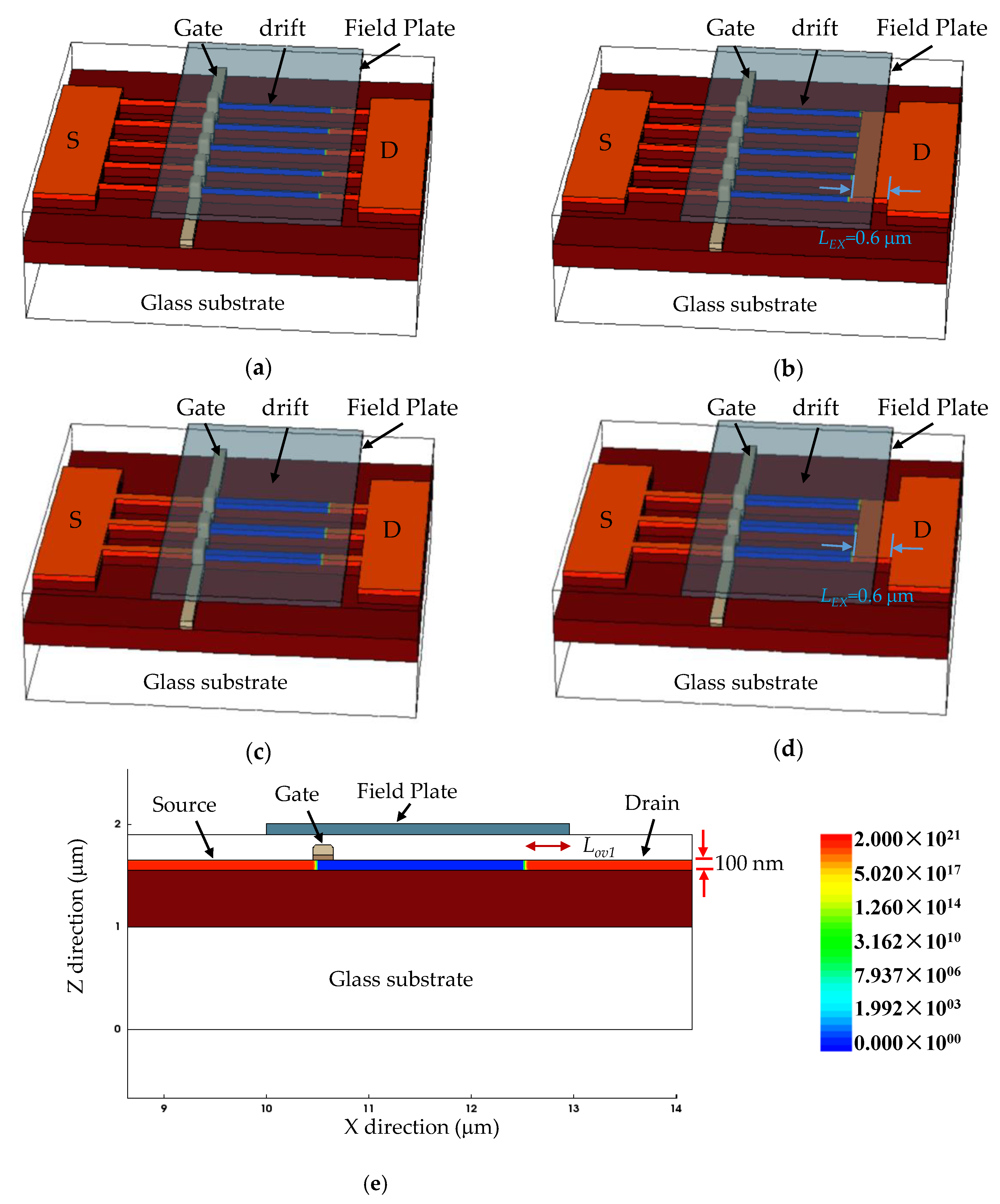
Figure 1 shows the 3-D structure of the FinTFTs with various extended wide drain lengths (LEX). The channel length (L) and height (h) are 0.2 μm and 100 nm, respectively. FinTFTs with different structures are simulated by varying each channel wire width (W0) and fin number Nf (i.e., W40: W0 = 40 nm, Nf = 5 and W200: W0 = 200 nm, Nf = 3). The effective channel width Weff is fixed at 1.2 μm (=(2h + W0) × Nf) for comparison. The LEX is from the drain region to the channel region and varies from 0 to 0.6 μm. The length of the overlap between the FP and N+ region (Lov1) is 0.5 μm, as shown in Figure 1e.
In this study, a Sentaurus technology computer aided design (TCAD) 3-D simulator was used. In the physic section of the device simulator, the mobility model, generation, and recombination models are included. For the mobility model, the “Doping Dependence”, “Enormal”, and “High Field Saturation” flags are used to consider mobility degradation due to impurity scattering, mobility degradation at the interfaces, and high electric field saturation, respectively. For generation and recombination models, “SRH”, “Auger”, “Avalanche”, and “Band 2 Band” flags are used to model the Shockley–Read–Hall recombination, Auger recombination, avalanche generation (impact ionization), and band-to-band tunneling, respectively.
3. Results and Discussion
3.1. Breakdown Characteristics
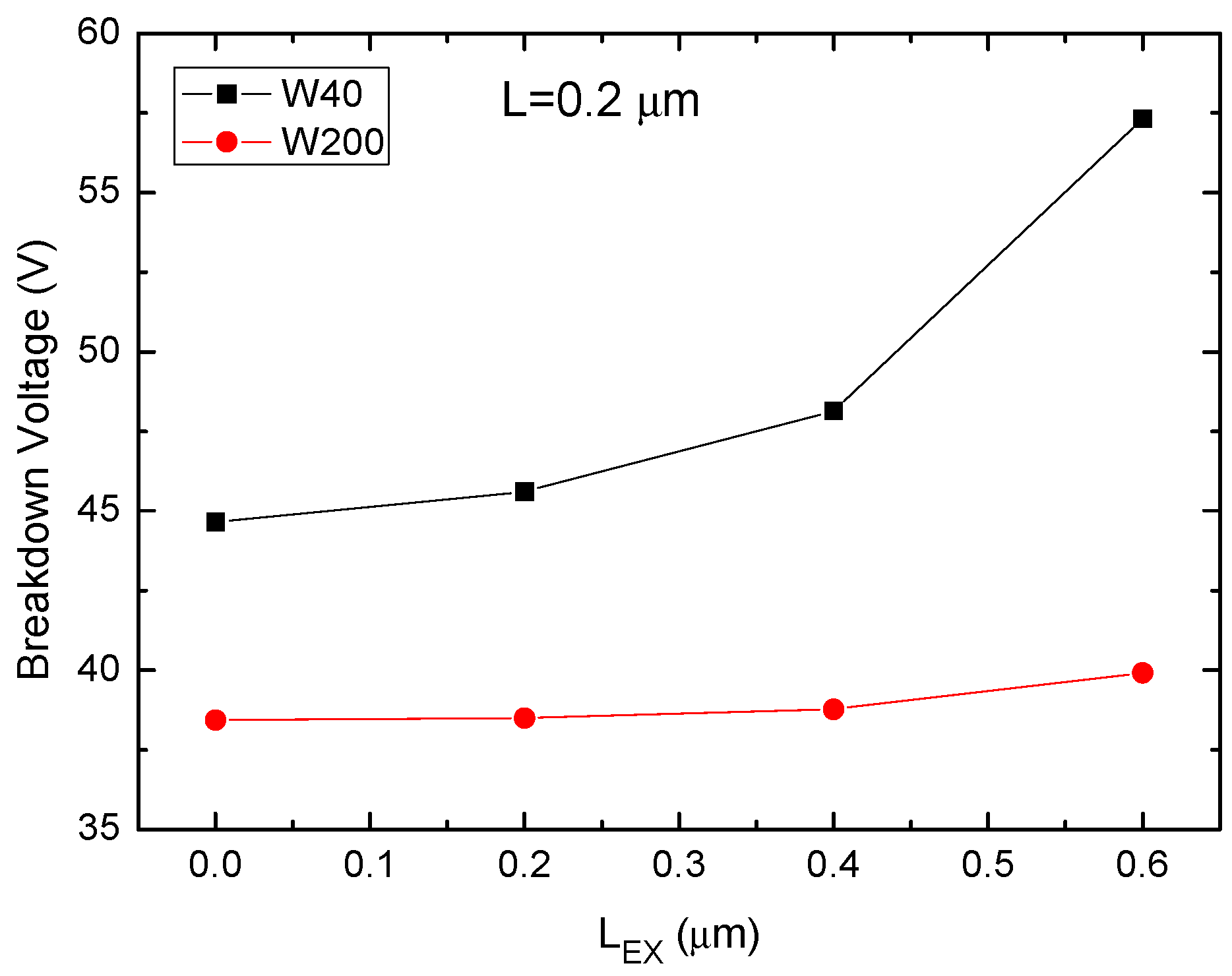
Figure 2a shows the breakdown voltage of W40 and W200 with various LEXs. When the drain current is 3 × 10⁻⁸ A, the breakdown voltage is taken as the drain voltage value at VGS = 0 V. For W40, the breakdown voltage increases when LEX increases from 0 to 0.6 μm. However, for W200, the influence of LEX on the breakdown voltage is quite small until LEX exceeds 0.6 μm. According to reports in the literature [40,41], a device with a narrower channel has a higher breakdown voltage due to a lower peak electric field, which is located near the drain; in addition, a device with a wider drift width has a lower electric field and impact ionization in the drift region, which results in a high breakdown voltage [42]. Here, a narrower channel in conjunction with a wider drain—for example, W40 with LEX = 0.6 μm—exhibits a high breakdown voltage (approximately 57 V).
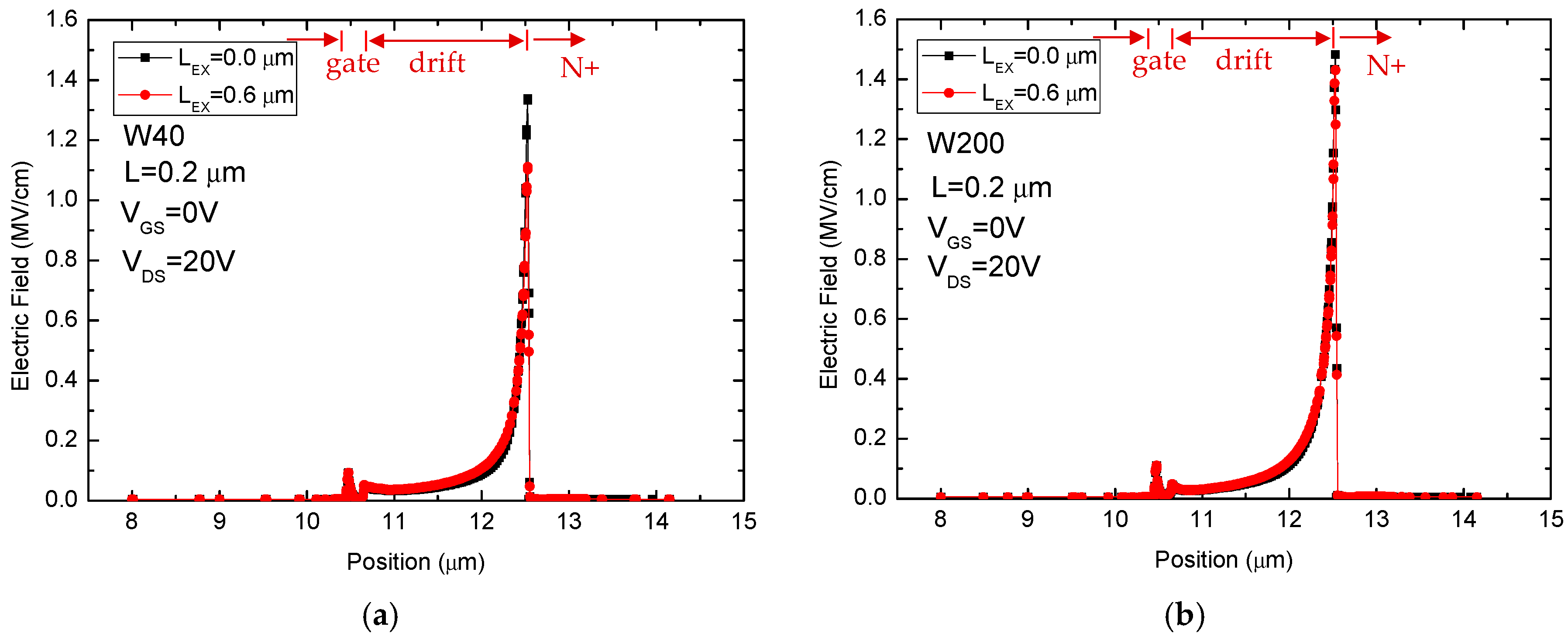
Figure 3 shows the electric field distribution of W40 and W200 with LEX = 0 and 0.6 μm at VGS = 0 V and VDS = 20 V (before breakdown). The highest electric field peaks of W40 and W200 are located at the intrinsic drift/N+ junction and cause breakdown. Suppressing the electric field peak at the intrinsic drift/N+ junction is an effective method for preventing breakdowns. In Figure 3a, it can be observed that extending the wide drain length of W40 to LEX = 0.6 μm led to a marked decrease in the electric field peak at the intrinsic/N+ junction and a consequent increase in the breakdown voltage. However, as each channel wire width increased, such as in W200, the difference in the electric field peak between LEX = 0 and 0.6 μm was not pronounced, as shown in Figure 3b. Additionally, the peak electric field values for W200 with LEX = 0 and 0.6 μm were 1.48 and 1.43 MV/m, respectively, compared with 1.34 and 1.11 MV/m, respectively, for W40 with LEX = 0 and 0.6 μm. The narrower each channel wire, the lower was the peak electric field. Therefore, the breakdown voltage of W40 was higher than that of W200. Consequently, extending the wide drain under the FP contributed to a more uniform electric field distribution within the drift region. Therefore, the breakdown voltage improved with an increase in LEX.
3.2. GIDL and ION/IOFF Ratio
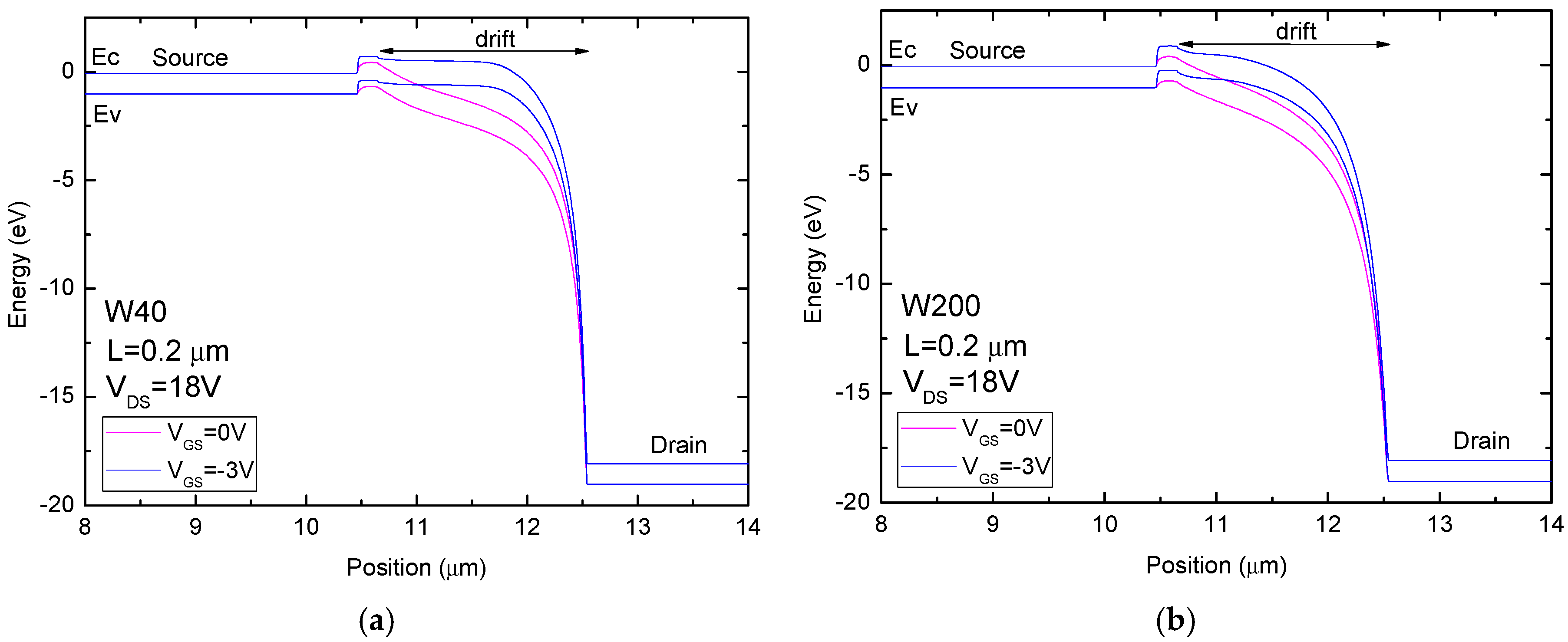
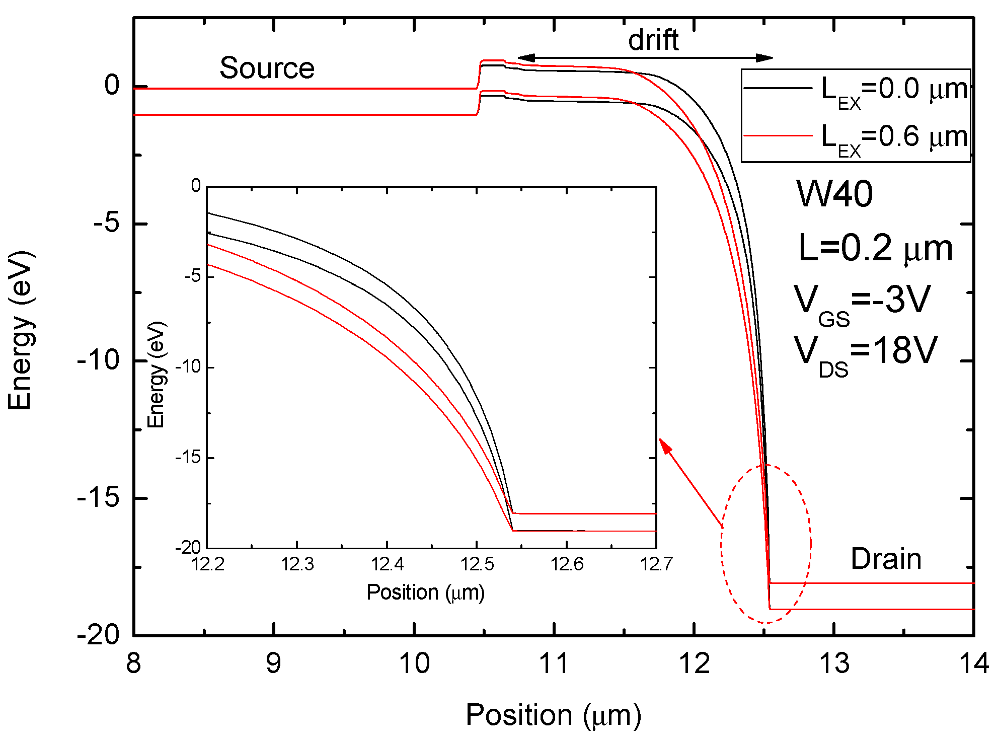
Figure 4a presents the typical subthreshold characteristics of FinTFTs with a narrow W0 (W40). The leakage current increased with a larger negative gate bias, which was due to GIDL. Increasing LEX can not only improve the breakdown voltage but also suppress GIDL. For multi-gate devices such as a FinFET with a narrow channel width, L-BTBT instead of conventional T-BTBT is dominant [31]. L-BTBT occurs when a high drain bias (VDS) and low gate bias (VGS) are applied and the valence band in the body becomes higher than the conduction band in the drain region; these factors increase the GIDL current. The typical subthreshold characteristics of a device with a wide W0 (W200) are shown in Figure 4b for comparison. The leakage current is almost constant below VGS = −1 V because of the slight change in the longitudinal energy band, which bends when VGS is varied. The longitudinal energy band diagrams of W40 and W200 with VGS = 0 and −3 V are presented in Figure 5. Weak gate controllability in W200, which is similar to that in the conventional planar structure, results in a minor influence of gate bias on the longitudinal energy band (Figure 5b). However, the bending of the longitudinal energy band becomes evident for W40 and is caused by a large longitudinal electrical field at the intrinsic drift /N+ junction (Figure 5a).
To understand the dependence of GIDL on LEX, the longitudinal energy band diagrams were analyzed. Figure 6 shows the longitudinal energy band diagrams of W40 with LEX = 0 and 0.6 μm at VGS = −3 V and VDS =18 V. For FinTFTs with LEX = 0.6 μm, an increase in the depletion width and a decrease in the electric field resulted in less pronounced band bending, and thus a wider tunneling width compared with FinTFTs with LEX = 0 μm.
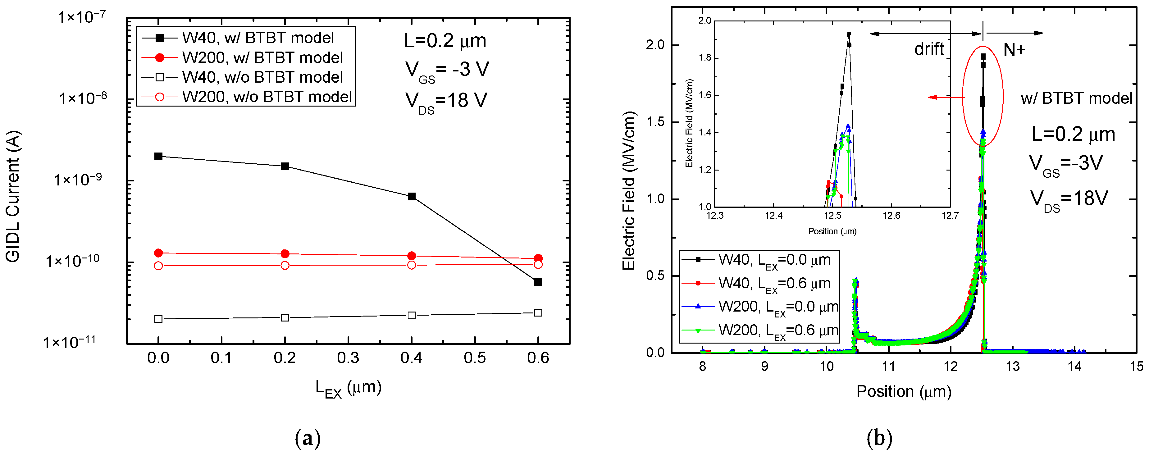
Figure 7a shows variation in the GIDL current with a wide drain length for W40 and W200 at VGS = −3 V and VDS = 18 V. The values in Figure 7a were obtained from the simulation results. The GIDL current of W40 and W200 without the BTBT model are also shown in Figure 7a. The GIDL current was almost constant when the BTBT model was not considered. The values for W40 and W200 are indicated by the black line with a hollow symbol and red line with a hollow symbol, respectively. W40 with LEX = 0 μm has a large GIDL current because of the enhanced L-BTBT. As a result, the GIDL current decreased as LEX increased. The GIDL current of W40 with LEX = 0.6 μm had a value close to that observed at the black line with a hollow symbol. However, the device with a wide W0 (W200) exhibited a small change in GIDL current with an increase in LEX, and all values of the GIDL current were close to the red line with a hollow symbol. Notably, the GIDL current of W40 with LEX = 0.6 μm was lower than that of W200; this indicates that a device with a wide drain can effectively reduce the GIDL current. Figure 7b shows the electric field distribution of W40 and W200 with LEX = 0 and 0.6 μm at VGS = −3 V and VDS = 18 V. The electric field peaks of W40 and W200 are located at the intrinsic drift/N+ junction. The peak value of the electrical field near the drain side can be expressed in the following relationship: W40/LEX = 0 μm > W200/LEX = 0 μm > W200/LEX = 0.6 μm > W40/LEX = 0.6 μm. The higher the electric field peaks, the higher is the GIDL current.
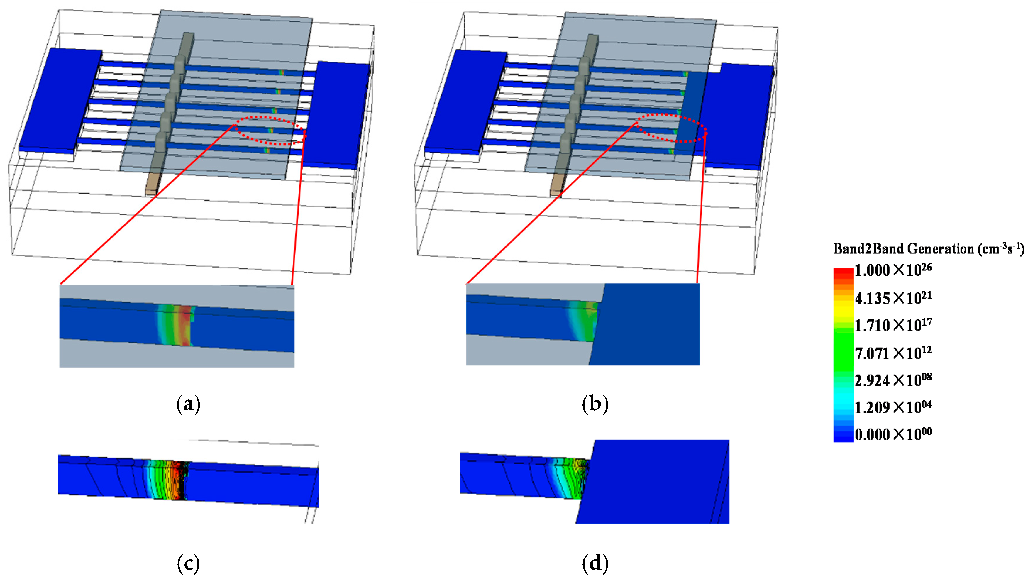
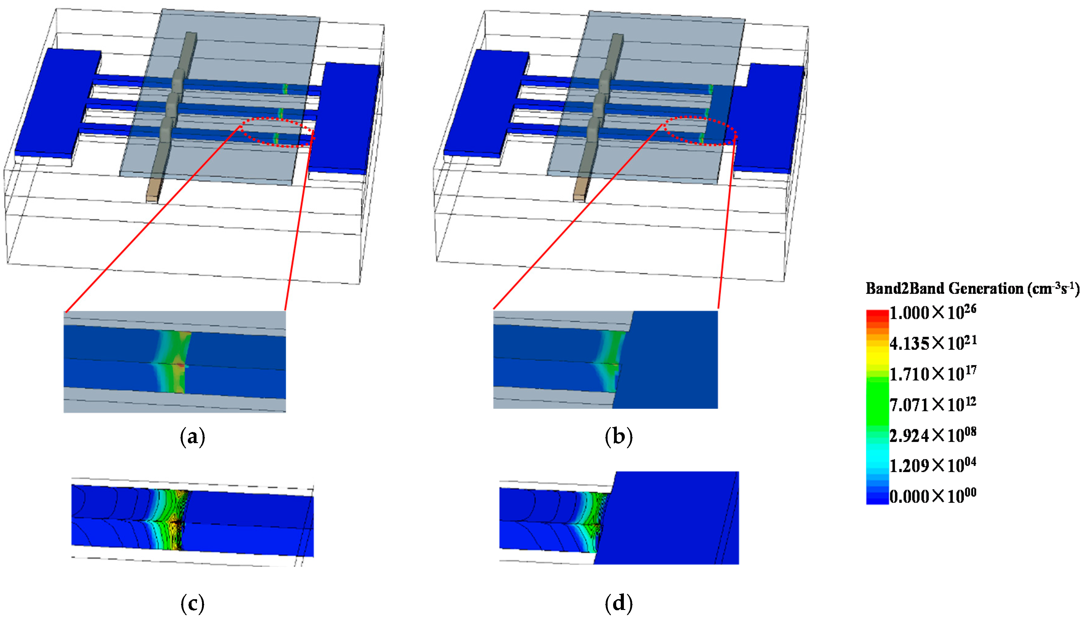
To clarify the improvement in the dependence of GIDL on LEX, the band-to-band generation rate (BTBT-GR) of W40 and W200 with LEX = 0 and 0.6 μm at VGS = −3 V and VDS = 18 V were analyzed to explain the correlation between GIDL and LEX, as shown in Figure 8 and Figure 9. The highest BTBT-GR for both W40 and W200 are located at the intrinsic drift/N+ junction, and its peaks are close to the surface at the drift/FP overlap region. The devices with LEX = 0.6 μm had a lower BTBT-GR compared with those with LEX = 0 μm, for which the GIDL was improved. Figure 8c and d show the BTBT-GR of W40 along with electric field contours near the intrinsic drift/N+ junction. The red area under the FP Is the dominant tunneling region of the FinTFT. Owing to the lower longitudinal electric field in the FinTFT with LEX = 0.6 μm, devices with extended wide drain were observed to have a lower GIDL. The BTBT-GR and electric field near the corner of W200 were higher than those towards the center, as shown in Figure 9c,d. In addition, the BTBT-GR, as well as the electric field in the corner of W40, were higher than those in the corner of W200. Therefore, W40 had a higher GIDL current than W200 owing to a higher BTBT-GR and the electric field near the corner.
Figure 10 shows the ION/IOFF ratio and ION of W40 with various LEX values at VDS = 18 V. The ON-state current (ION) is obtained at VGS = 3 V, and the off-state current (IOFF) is obtained at VGS = 0 V. As the LEX increases, so does the ION of W40 with GFP and the ION/IOFF ratio (shown in Figure 10a). Extending the wide drain region length leads to a large cross section in the current path and increases the ION. However, when the FP is applied to extra-high voltage (VFP = 30 V) instead of the gate voltage, the ION slightly decreases as the LEX increases, as shown in Figure 5b. According to a previous study [26], when VFP = 30 V, FinTFTs with wide drift have a high electron density concentrated at the corner of the drift and a low electron density at the non-corner region. Nevertheless, as the drift region of FinTFTs changed to multiple nanowire and each wire width was downscaled to nanometers, the corner and non-corner regions exhibited high electron density. Lower electron density in the FinTFTs with a wide drift (LEX = 0.6 μm) leads to a low ION. Therefore, the ION of FinTFTs with LEX = 0 μm is higher than that of that with LEX = 0.6 μm. The FinTFTs with GFP not only achieved a high ION and ION/IOFF ratio but also required no external bias.
4. Conclusions
An investigation of breakdown voltage, GIDL, and ON-state current in tri-gate FinTFTs with various LEX was conducted using 3-D simulations. This short channel (L = 0.2 μm) is composed of a FinTFT contains multi-gate, which enables the suppression of short channel effects, and a wide drain, which reduces the longitudinal electric field at the intrinsic drift /N+ junction and improves GIDL and the breakdown characteristics. By extending the wide drain region length, the electric field peak was effectively suppressed, as was L-BTBT-induced GIDL. Furthermore, the wide drain FinTFTs with GFP exhibited higher ON-state currents and required no external bias. As the technology node is further scaled down, FinTFTs with wide drains demonstrate their potential for use as TFTs in SoP applications.
Author Contributions
H.-H.H. conceived and designed the experiments; H.-H.H. and Y.-W.Z. ran the simulation; H.-H.H. and Y.-W.Z. performed the electrical characterization; H.-H.H. and Y.-W.Z. analyzed the data; H.-H.H. and K.-M.C. supervised the project; H.-H.H. and Y.-W.Z. wrote the manuscript; and all authors contributed discussions and feedback to the manuscript and the project.
Funding
This work was supported by Ministry of Science and Technology of Taiwan under Contract MOST 106-2221-E-027-123 and MOST-106-2218-E-027-002 and is also conducted under the “Real-Time Situation Awareness Subsystem Technologies for Automatic Driving Project” of the Institute for Information Industry which is subsidized by the Ministry of Economic Affairs of the Republic of China.
Acknowledgments
The authors would like to thank the National Center for High-Performance Computing for computer time and facilities.
Conflicts of Interest
The authors declare no conflict of interest.
References
- Kuo, P.Y.; Lin, J.Y.; Chao, T.S. Implantation free GAA double spacer poly-Si nanowires channel junctionless FETs with sub-1V gate operation and near ideal subthreshold swing. In Proceedings of the IEEE IEDM, Washington, DC, USA, 7–9 December 2015; pp. 631–634. [Google Scholar] [CrossRef]
- Hung, M.F.; Wu, Y.C.; Tien, S.C.; Chen, J.H. Polycrystalline-Si TFT TANOS flash memory cell with Si nanocrystals for high program/erase speed and good retention. IEEE Electron Device Lett. 2012, 33, 649–651. [Google Scholar] [CrossRef]
- Chen, Y.J.E.; Lee, Y.J.; Yu, Y.H. Investigation of polysilicon thin-film transistor technology for RF applications. IEEE Trans. Microw. Theory Tech. 2010, 58, 3444. [Google Scholar] [CrossRef]
- Yu, Y.H.; Lee, Y.J.; Li, Y.H.; Kuo, C.H.; Li, C.H.; Hsieh, Y.J.; Liu, C.T.; Chen, Y.J.E. An LTPS TFT Demodulator for RFID Tags Embeddable on Panel Displays. IEEE Trans. Microw. Theory Tech. 2009, 57, 1356–1361. [Google Scholar] [CrossRef]
- Vidor, F.F.; Meyers, T.; Hilleringmann, U. Inverter circuits using ZnO nanoparticle based thin-film transistors for flexible electronic applications. Nanomaterials 2016, 6, 154. [Google Scholar] [CrossRef] [PubMed]
- Chen, K.N.; Yang, C.F.; Wu, C.C.; Chen, Y.H. Development of the α-IGZO/Ag/α-IGZO triple-layer structure films for the application of transparent electrode. Materials 2017, 10, 226. [Google Scholar] [CrossRef] [PubMed]
- Martins, J.; Bahubalindruni, P.; Rovisco, A.; Kiazadeh, A.; Martins, R.; Fortunato, E.; Barquinha, P. Bias stress and temperature impact on InGaZnO TFTs and circuits. Materials 2017, 10, 680. [Google Scholar] [CrossRef] [PubMed]
- Fan, C.L.; Tseng, F.P.; Tseng, C.Y. Electrical performance and reliability improvement of amorphous-indium-gallium-zinc-oxide thin-film transistors with HfO2 gate dielectrics by CF4 plasma treatment. Materials 2018, 11, 824. [Google Scholar] [CrossRef] [PubMed]
- Huang, T.Y.; Lewis, A.G.; Chiang, A.; Wu, I.W.; Koyanagi, M. A new implant-through-contact method for fabricating high-voltage TFTs. IEEE Electron Device Lett. 1988, 9, 347–349. [Google Scholar] [CrossRef]
- Hack, M.; Chiang, A.; Huang, T.Y.; Lewis, A.G.; Martin, R.A.; Tuan, H.; Wu, I.W.; Yap, P. High-voltage thin film transistors for large area microelectronics. In Proceedings of the IEEE IEDM, San Francisco, CA, USA, 11–14 December 1988; pp. 252–255. [Google Scholar] [CrossRef]
- Unagami, T.; Tsujiyama, B. High-voltage silicon thin film transistor on quartz. IEEE Electron Device Lett. 1982, 3, 167–168. [Google Scholar] [CrossRef]
- Tanaka, K.; Arai, H.; Kohda, S. Characteristics of offset-structure polycrystalline-silicon thin-film transistors. IEEE Electron Device Lett. 1988, 9, 23–25. [Google Scholar] [CrossRef]
- Clough, F.J.; Narayanan, E.M.S.; Chen, Y.; Eccleston, W.; Milne, W.I. Polycrystalline silicon thin film transistor incorporating a semi-insulating field plate for high voltage circuitry on glass. Appl. Phys. Lett. 1997, 71, 2002–2004. [Google Scholar] [CrossRef]
- Xu, Y.Z.; Clough, F.J.; Narayanan, E.M.S.; Chen, Y.; Milne, W.I. A conductivity modulated high voltage polycrystalline silicon thin film transistor with improved on state and transient performance. In Proceedings of the IEEE IEDM, San Francisco, CA, USA, 6–9 December 1998; pp. 273–276. [Google Scholar] [CrossRef]
- Huang, T.Y.; Wu, I.W.; Lewis, A.G.; Chiang, A.; Bruce, R.H. A simpler 100-V polysilicon TFT with improved turn-on characteristics. IEEE Electron Device Lett. 1990, 11, 244–246. [Google Scholar] [CrossRef]
- Kim, S.Y.; Loke, W.F.; Jung, B.; Roy, K. High-frequency modeling of poly-Si thin-film transistors for low-cost RF applications. IEEE Trans. Electron Devices 2012, 59, 2296–2301. [Google Scholar] [CrossRef]
- Oh, S.H.; Monroe, D.; Hergenrother, J.M. Analytic description of short-channel effects in fully-depleted Double-Gate and cylindrical, surrounding-gate MOSFETs. IEEE Electron Device Lett. 2000, 21, 445–447. [Google Scholar] [CrossRef]
- Chang, L.; Tang, S.; King, T.J.; Hu, C. Gate length scaling and threshold voltage control of double-gate MOSFETs. In Proceedings of the IEEE IEDM, San Francisco, CA, USA, 10–13 December 2000; pp. 719–722. [Google Scholar] [CrossRef]
- Hisamoto, D.; Lee, W.; Kedzierski, J.; Takeuchi, H.; Asano, K.; Kuo, C.; Anderson, E.; King, T.J.; Bokor, J.; Hu, C. FinFET—a self-aligned double-gate MOSFET scalable to 20 nm. IEEE Trans. Electron Device 2000, 12, 2320–2325. [Google Scholar] [CrossRef]
- Rios, R.; Cappellani, A.; Armstrong, M.; Budrevich, A.; Gomez, H.; Pai, R.; Rahhal-orabi, N.; Kuhn, K. Comparison of junctionless and conventional trigate transistors with Lg down to 26 nm. IEEE Electron Device Lett. 2011, 32, 1170–1172. [Google Scholar] [CrossRef]
- Barraud, S.; Berthomé, M.; Coquand, R.; Cassé, M.; Ernst, T.; Samson, M.P.; Perreau, P.; Bourdelle, K.K.; Faynot, O.; Poiroux, T. Scaling of trigate junctionless nanowire MOSFET with gate length down to 13 nm. IEEE Electron Device Lett. 2012, 33, 12251227. [Google Scholar] [CrossRef]
- Liao, T.C.; Tu, S.W.; Yu, M.H.; Lin, W.K.; Liu, C.C.; Chang, K.J.; Tai, Y.H.; Cheng, H.C. Novel gate-all-around poly-Si TFTs with multiple nanowire channels. IEEE Electron Device Lett. 2008, 29, 889. [Google Scholar] [CrossRef]
- Lu, Y.H.; Kuo, P.Y.; Wu, Y.H.; Chen, Y.H.; Chao, T.S. NoNovel sub-10-nm gate-all-around Si nanowire channel poly-Si TFTs with raised source/drain. IEEE Electron Device Lett. 2011, 32, 173–175. [Google Scholar] [CrossRef]
- Narimani, K.; Trellenkamp, S.; Tiedemann, A.; Mantl, S.; Zhao, Q.T. Strained silicon single nanowire gate-all-around TFETs with optimized tunneling junctions. Appl. Sci. 2018, 8, 670. [Google Scholar] [CrossRef]
- Chen, J.; Chan, T.Y.; Chen, I.C.; Ko, P.K.; Hu, C. Subbreakdown drain leakage current in MOSFET. IEEE Electron Device Lett. 1987, 11, 515–517. [Google Scholar] [CrossRef]
- Chan, T.Y.; Chen, J.; Ko, P.K.; Hu, C. The impact of gate-induced leakage current on MOSFET scaling. In Proceedings of the IEEE IEDM, Washington, DC, USA, 6–9 December 1987; pp. 718–721. [Google Scholar]
- Wann, H.; Ko, P.K.; Hu, C. Gate-induced band-to-band tunneling leakage current in LDD MOSFETs. In Proceedings of the IEEE IEDM, San Francisco, CA, USA, 13–16 December 1992; pp. 147–150. [Google Scholar]
- Fan, J.; Li, M.; Xu, X.; Huang, R. New observation on gate-induced drain leakage in Silicon nanowire transistors with Epi-Free CMOS compatible technology on SOI substrate. In Proceedings of the IEEE SOI-3D-Subthreshold Microelectronics Technology Unified Conference (S3S), Monterey, CA, USA, 7–10 October 2013; pp. 1–2. [Google Scholar]
- Fan, J.; Ming, L.; Xiaoyan, X.; Yuancheng, Y.; Haoran, X.; Ru, H. Insight Into gate-induced drain leakage in silicon nanowire transistors. IEEE Trans. Electron Device 2015, 62, 213–219. [Google Scholar]
- Sahay, S.; Kumar, M.J. A novel gate-stack-engineered nanowire FET for scaling to the sub-10-nm regime. IEEE Trans. Electron Device 2016, 63, 5055–5059. [Google Scholar] [CrossRef]
- Sahay, S.; Kumar, M.J. Insight into lateral band-to-band-tunneling in nanowire junctionless FETs. IEEE Trans. Electron Device 2016, 63, 4138–4142. [Google Scholar] [CrossRef]
- Hur, J.; Lee, B.H.; Kang, M.H.; Ahn, D.C.; Bang, T.; Jeon, S.B. Comprehensive analysis of gate-induced drain leakage in vertically stacked nanowire FETs: inversion-mode versus junctionless mode. IEEE Electron Device Lett. 2016, 37, 541–544. [Google Scholar] [CrossRef]
- Sahay, S.; Kumar, M.J. Spacer design guidelines for nanowire FETs from gate-induced drain leakage perspective. IEEE Trans. Electron Device 2017, 64, 3007–3015. [Google Scholar] [CrossRef]
- Sahay, S.; Kumar, M.J. Physical insights into the nature of gate-induced drain leakage in ultrashort channel nanowire FETs. IEEE Trans. Electron Device 2017, 64, 2604–2610. [Google Scholar] [CrossRef]
- Tsai, J.Y.; Hu, H.H.; Wu, Y.C.; Jhan, Y.R.; Chen, K.M.; Huang, G.W. A novel hybrid poly-Si nanowire LDMOS with extended drift. IEEE Electron Device Lett. 2014, 35, 366–368. [Google Scholar] [CrossRef]
- Tsai, J.Y.; Hu, H.H. Novel gate-all-around high-voltage thin-film transistor with t-shaped metal field plate design. IEEE Trans. Electron Device 2015, 62, 882–887. [Google Scholar] [CrossRef]
- Auth, C.; Cappellani, A.; Chun, J.; Dalis, A.; Davis, A.; Ghani, T.; Glass, G.; Glassman, T.; Harper, M.; Hattendorf, M. 45 nm high-K metal gate strain-enhanced transistors. In Proceedings of the Symposium on VLSI Technology, Honolulu, HI, USA, 17–19 June 2008; pp. 128–129. [Google Scholar]
- Kesapragada, S.; Wang, R.; Liu, D.; Liu, G.; Xie, Z.; Ge, Z.; Yang, H.; Lei, Y.; Lu, X.; Tang, X.; et al. High-k/metal gate stacks in gate first and replacement gate schemes. In Proceedings of the IEEE/SEMI Advanced Semiconductor Manufacturing Conference (ASMC), San Francisco, CA, USA, 11–13 July 2010; pp. 256–259. [Google Scholar]
- Jan, C.H.; Agostinelli, M.; Deshpande, H.; El-Tanani, M.A. RF CMOS technology scaling in high-k/metal gate era for RF SoC (system-on-chip) applications. In Proceedings of the IEEE International Electron Devices Meeting, San Francisco, CA, USA, 6–8 December 2010; pp. 604–607. [Google Scholar]
- Duan, F.L.; Zhao, X.; Ioannou, D.E. Increased channel edge impact ionization in SOI MOSFET’s and effects on device operation. In Proceedings of the IEEE International SOI Conference Proceedings, Stuart, FL, USA, 5–8 October 1998; pp. 171–172. [Google Scholar]
- Lee, C.W.; Afzalian, A.; Yan, R.; Akhavan, N.D.; Xiong, W.; Colinge, J.P. Drain breakdown voltage in MuGFETs: Influence of physical parameters. IEEE Trans. Electron Device 2008, 55, 3503–3506. [Google Scholar] [CrossRef]
- Chen, K.M.; Chen, B.Y.; Chiu, C.S.; Huang, G.W.; Chen, C.H.; Lin, H.C.; Huang, T.Y.; Chen, M.Y.; Yang, Y.C.; Jaw, B.; et al. Performance improvement in RF LDMOS transistors using wider drain contact. IEEE Electron Device Lett. 2013, 34, 1085–1087. [Google Scholar] [CrossRef]
Figure 1.
3-D structure of FinTFTs: (a) W40 with LEX = 0 μm; (b) W40 with LEX = 0.6 μm; (c) W200 with LEX = 0 μm; and (d) W200 with LEX = 0.6 μm; (e) Cross-section view of FinTFT.
Figure 1.
3-D structure of FinTFTs: (a) W40 with LEX = 0 μm; (b) W40 with LEX = 0.6 μm; (c) W200 with LEX = 0 μm; and (d) W200 with LEX = 0.6 μm; (e) Cross-section view of FinTFT.

Figure 2.
Breakdown voltage of FinTFTs with various LEX.

Figure 3.
Electric field distribution of (a) W40 and (b) W200 with LEX = 0 and LEX = 0.6 μm at VDS = 20 V (before breakdown).
Figure 3.
Electric field distribution of (a) W40 and (b) W200 with LEX = 0 and LEX = 0.6 μm at VDS = 20 V (before breakdown).

Figure 4.
Subthreshold characteristics of (a) W40 and (b) W200 with various LEX at VDS = 18 V.

Figure 5.
Longitudinal energy band diagrams of (a) W40 and (b) W200 with VGS = 0 and −3 V.

Figure 6.
Longitudinal energy band diagrams of W40 with LEX = 0 and LEX = 0.6 μm at VGS = −3 V and VDS = 18 V.
Figure 6.
Longitudinal energy band diagrams of W40 with LEX = 0 and LEX = 0.6 μm at VGS = −3 V and VDS = 18 V.

Figure 7.
(a) Variation in the GIDL current with a wide drain length for W40 and W200 at VGS = −3 V and VDS = 18 V. (b) Electric field distribution of W40 and W200 with LEX = 0 and 0.6 μm at VGS = −3 V and VDS = 18 V.
Figure 7.
(a) Variation in the GIDL current with a wide drain length for W40 and W200 at VGS = −3 V and VDS = 18 V. (b) Electric field distribution of W40 and W200 with LEX = 0 and 0.6 μm at VGS = −3 V and VDS = 18 V.

Figure 8.
BTBT-GR of W40 with (a) LEX = 0 μm and (b) LEX = 0.6 μm and 3-D profile with electric field contours for (c) LEX = 0 μm and (d) LEX = 0.6 μm.
Figure 8.
BTBT-GR of W40 with (a) LEX = 0 μm and (b) LEX = 0.6 μm and 3-D profile with electric field contours for (c) LEX = 0 μm and (d) LEX = 0.6 μm.

Figure 9.
BTBT-GR of W200 with (a) LEX = 0 μm and (b) LEX = 0.6 μm and 3-D profile with electric field contours for (c) LEX = 0 μm and (d) LEX = 0.6 μm.
Figure 9.
BTBT-GR of W200 with (a) LEX = 0 μm and (b) LEX = 0.6 μm and 3-D profile with electric field contours for (c) LEX = 0 μm and (d) LEX = 0.6 μm.

Figure 10.
On-state current and ION/IOFF ratio of W40 with various LEX at VDS = 18 V. (a) Gate field plate (GFP) and (b) VFP = 30 V.
Figure 10.
On-state current and ION/IOFF ratio of W40 with various LEX at VDS = 18 V. (a) Gate field plate (GFP) and (b) VFP = 30 V.

© 2018 by the authors. Licensee MDPI, Basel, Switzerland. This article is an open access article distributed under the terms and conditions of the Creative Commons Attribution (CC BY) license (http://creativecommons.org/licenses/by/4.0/).
Share and Cite
MDPI and ACS Style
Hu, H.-H.; Zeng, Y.-W.; Chen, K.-M. Improving the Gate-Induced Drain Leakage and On-State Current of Fin-Like Thin Film Transistors with a Wide Drain. Appl. Sci. 2018, 8, 1406. https://0-doi-org.brum.beds.ac.uk/10.3390/app8081406
AMA Style
Hu H-H, Zeng Y-W, Chen K-M. Improving the Gate-Induced Drain Leakage and On-State Current of Fin-Like Thin Film Transistors with a Wide Drain. Applied Sciences. 2018; 8(8):1406. https://0-doi-org.brum.beds.ac.uk/10.3390/app8081406
Chicago/Turabian StyleHu, Hsin-Hui, Yan-Wei Zeng, and Kun-Ming Chen. 2018. "Improving the Gate-Induced Drain Leakage and On-State Current of Fin-Like Thin Film Transistors with a Wide Drain" Applied Sciences 8, no. 8: 1406. https://0-doi-org.brum.beds.ac.uk/10.3390/app8081406
Note that from the first issue of 2016, this journal uses article numbers instead of page numbers. See further details here.