Excimer Laser Three-Dimensional Micromachining Based on Image Projection and the Optical Diffraction Effect

Department of Mechanical Engineering, Cheng Kung University, Tainan 701, Taiwan
*
Author to whom correspondence should be addressed.
Appl. Sci. 2018, 8(9), 1690; https://0-doi-org.brum.beds.ac.uk/10.3390/app8091690
Submission received: 31 July 2018
/
Revised: 8 September 2018
/
Accepted: 13 September 2018
/
Published: 18 September 2018
(This article belongs to the Section Optics and Lasers)
Abstract
:An excimer laser three-dimensional (3D) micromachining system is proposed based on a mask image projection method and the optical diffraction effect. The effects of optical diffraction on the laser machining rate are evaluated using a hole-arrayed mask pattern with various feature sizes and hole-area opening ratios. The practical feasibility of the proposed method is demonstrated by machining conical, trihedral, and pyramidal 3D microstructures on polycarbonate substrates. The proposed method greatly simplifies the photo-mask design and preparation task in traditional excimer laser 3D micromachining systems and provides a powerful technique for achieving large-area 3D microstructures with complex patterns and atypical profiles.
1. Introduction
The direct machining of microstructures by pulsed excimer lasers has attracted significant interest over the past 30 years or so [1,2,3]. Figure 1 presents a schematic illustration of a typical excimer laser micromachining system based on a mask projection approach [4,5]. As shown, the system consists of an excimer laser source, a laser beam homogenizer, a photo-mask, an optical image projection system, and a multi-axis translation stage. Typically, the laser source is provided by ArF (193 nm), KrF (248 nm), or XeF (308 nm) pulsed lasers, which emit a continuous train of short pulses with a high energy. The laser beam homogenizer re-shapes the laser beam profile such that a uniform laser intensity distribution is obtained on the photo-mask surface. The light passing through the mask is projected by an optical imaging system onto the surface of the sample, which is mounted on a servo-controlled multi-axis translation stage. The whole system is operated under the control of a personal computer, which synchronizes the laser firing sequence and the sample movement during the machining process in such a way as to achieve the required micromachined features on the substrate surface.
Femtosecond lasers are also used in micro-machining based on cold ablation. When materials are radiated by laser pulses with ultrashort pulse duration (a few hundred or tens of femtoseconds), the heat-affected zone (HAZ) is negligible, so cold laser ablation is achieved [6]. However, in some cases the femtosecond lasers operate with a higher pulse repetition rate (up to 100 kHz or less) to increase the machining rate, and the heat effect becomes significant. In other words, it is a trade-off between machining quality and machining time. Furthermore, most femtosecond lasers are still used for 2D machining or direct patterning while in this work we are focused on machining 3D-microstructures based on optical diffraction modulation.
The mask projection system shown in Figure 1 was intended originally for two-dimensional (2D) micromachining. In such a system, the machined area on the sample surface has the same dimensions as those of the photo-mask pattern other than for the de-magnification effect of the optical imaging system. Since the wavelength of excimer lasers is typically in the deep ultraviolet (UV) region, the photon energy can be high (5 eV for KrF-248 nm, for example), so certain covalent bonds in polymer substrates (polycarbonate, polyimide, etc.) are broken directly when subjected to laser irradiation. This phenomenon is known as photochemical laser ablation and is favorable in laser machining due to the minimal thermal damage and burning which it causes. When applying pulsed excimer lasers to certain polymer materials, the photochemical etching effect dominates the laser ablation process and results in the formation of smooth and clearly defined micro-features. Since the laser fluence projected onto the sample surface is uniform, each laser pulse removes a constant depth of material over the projected image area. In practice, the laser machining rate depends on both the projected laser fluence and the material properties of the sample. By firing a continuous train of laser pulses, material removal is carried out layer by layer and the machining depth accumulates proportionally. The final laser-machined 2D microstructures have a surface pattern defined by the photo-mask design and a machining depth (or structure height) determined by the number of laser pulses received at each particular point on the substrate surface and the laser machining rate.
The literature contains various proposals for 3D micromachining systems based on the configuration shown in Figure 1. Broadly speaking, these systems fall into two main categories depending on the characteristics of the photo-mask used in the ablation process, namely binary or grey-scale. When using a binary photo-mask (typically a thin layer of chrome patterned on a quartz substrate), the 3D microstructures are obtained through a careful control of the relative movement between the laser-projected photo-mask pattern and the sample under a specific firing sequence of laser pulses. This technique, known as contour mask scanning [7,8,9,10,11,12,13,14,15], results in the formation of a 3D machined profile through the superposition of multiple 2D machined patterns appropriately distributed at different locations and orientations. In general, achieving a specific 3D machined profile requires a careful design of both the photo-mask pattern and the scanning path. When applying this method to realize arrayed 3D microstructures, the scanning path usually has the form of straight lines along two or three directions. Such a technique is known as laser dragging and has found widespread use for the patterning of rectangular and hexagonal arrays of microlenses with various aspherical surface profiles [16,17].
In 3D excimer laser micromachining systems of the second type, the ablation process is performed using a grey-scale or half-tone mask [18,19,20,21]. These masks locally vary (i.e., modulate) the transmission coefficient of the laser light incident on the mask surface such that the distribution of the laser fluence on the sample can be directly controlled. Thus, through an appropriate design of the projected laser fluence and laser machining rate, the distribution of the machining depth on the sample can be varied as required to realize micro-features with different 3D profiles. However, in implementing such systems, designing suitable transmission-varying masks poses a significant challenge. In practice, obtaining a true grey-scale mask is very difficult, so most experimental systems utilize half-tone masks, namely binary masks containing arrayed micro-patterns with feature sizes smaller than the resolution of the optical imaging system. By locally adjusting the feature size, the projected laser fluence can be effectively altered point by point, thereby achieving the goal of 3D micromachining. Compared to the contour mask scanning method, half-tone mask methods are both more direct and more straightforward. Furthermore, they enable the fabrication of 3D micro-structures with complicated surface profiles, which are often difficult (or even impossible) to achieve using mask contour scanning techniques. However, these performance advantages come at the expense of a greater cost since such masks typically have tiny characteristic feature sizes less than 1 μm.
Regardless of the type of mask and/or method used to perform image-projected laser machining, the optical diffraction effect plays a critical role in determining the final 3D micromachining outcome. In the contour mask scanning method, diffraction occurs at the rim of the open aperture in the photo-mask pattern, and results in the formation of a transition zone at the perimeter of the projected machining area on the sample surface. The machining depth within this transition zone is, strictly speaking, no longer digital or binary, but has the form of a slope. In practice, this optical diffraction effect is very important in achieving an analog 3D machined profile in contour mask scanning methods since it reduces the surface step size between adjacent laser shots and improves the machined surface roughness as a result. When using a half-tone mask, the optical diffraction phenomenon is even more important since the 3D laser machining process is based intrinsically on the optical diffraction effect. However, even though several authors have provided basic guidelines for half-tone mask designs, the literature lacks the feasibility of exploiting optical diffraction effect to achieve complex-geometry 3D microstructures.
Accordingly, the present study performs an experimental investigation into the effects of optical diffraction on the machining capabilities of a 3D excimer laser micromachining system using a binary photo-mask. The blurring effect caused by optical diffraction is generally regarded as non-desirable in optical imaging systems. However, in this study, it is shown that, through an appropriate control of the optical diffraction effect, complex 3D micromachined patterns can be realized without the need for an expensive and small line-width photo-mask. The remainder of this paper is organized as follows. Section 2 quantitatively examines the effects of optical diffraction using a binary hole-array mask pattern. Section 3 demonstrates the practical feasibility of the proposed diffraction-based excimer laser micromachining system by fabricating conical, trihedral, and pyramidal 3D micro-structures on polycarbonate substrates. Finally, Section 4 provides brief concluding remarks.
2. The Excimer Laser Micromachining System and the Optical Diffraction Effect
The micromachining trials were conducted using the excimer laser system shown in Figure 1. (For full details, refer to [14,15,16].) The system was implemented using a KrF laser source (COMPex Pro 210, Lambda Physik, Goettingen, Germany) with a wavelength of 248 nm. The laser was passed through a telescope lens system and an optical homogenizer to form a uniform flat-top laser energy distribution over a cross-sectional area of 1.5 × 1.5 cm2 on the photo-mask surface. The light passing through the photo-mask was projected onto the sample surface with a 10X de-magnification factor using a high-resolution projection lens system (P-Lens 4-10X/4-xxx, P/N_M290009, Lambda Physik, Goettingen, Germany). The sample was placed on a 4-axis (x-y-z-θ) servo-controlled automatic stage. During the machining process, the stage motion and laser firing sequence were controlled by a personal computer.
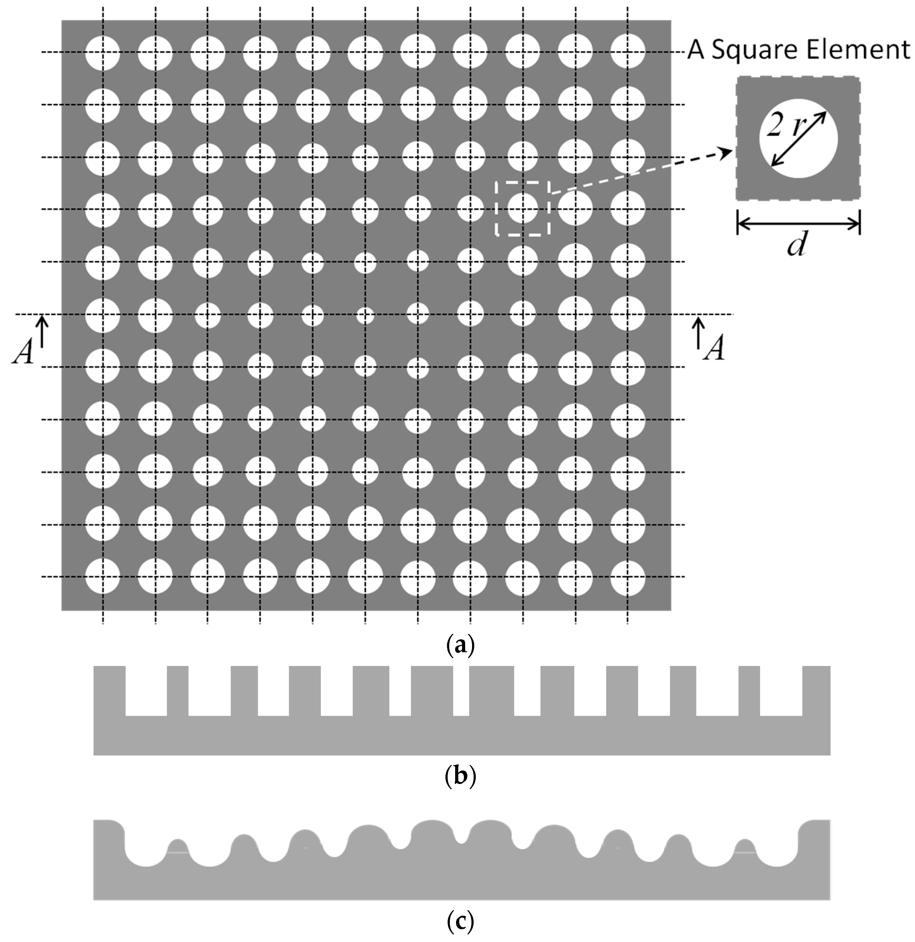
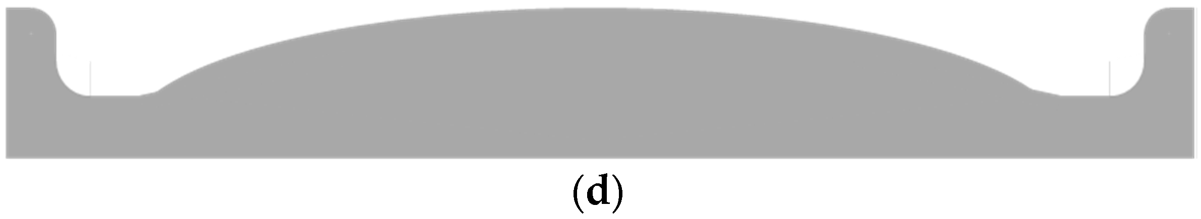
Figure 2a presents a schematic illustration of the hole-array mask pattern used to perform the micromachining process. As shown, the mask contains a rectangular array of square elements, with each element having a hole-opening aperture located at its center. For convenience, the side-length dimension of the square elements is denoted as d, while the hole radius is denoted as r. In designing the mask, the element size (d) was assigned a constant value, while the hole-radius (r) was varied so as to achieve a local variation in the optical transmission. Figure 2b,d provides qualitative illustrations of the laser-machined cross-sectional profiles obtained using the elements located along Section A-A of the photo-mask shown in Figure 2a given optical diffraction effects with different intensities. Figure 2b shows the machined profile for the case of negligible optical diffraction. It is observed that the micromachined features have a perfect binary characteristic, i.e., sharp edges and corners. However, while this situation represents the ideal case for 2D machining, it cannot be achieved in practice since the optical diffraction effect can never be entirely eliminated. As the intensity of the optical diffraction effect increases (i.e., the feature size in the photo-mask pattern decreases), a noticeable rounding of the edges and corners occurs. In the case of Figure 2c, the diffraction effect is relatively mild, so the machined profiles are still dominated by the hole-array mask pattern. However, as the feature size of the hole-array mask pattern reduces, the diffraction effect increases to such an extent that the machined depth and machined profiles are determined by an analog distribution of the diffracted laser energy. Thus, as shown in Figure 2d, individual hole features are no longer apparent in the machined surface profile. Rather, the neighboring hole features merge into one another, through optical diffraction of the image projection system, and with the machined depth determined by the projected laser energy at the corresponding position on the sample surface. It is noted that this result is typical of that achieved by 3D micromachining systems using a grey-tone or half-tone mask.
The schematic presented in Figure 2 show that the optical diffraction effect must be quantitatively determined before an excimer laser machining system can be used in real-world 3D micromachining applications. Accordingly, 5″ Cr/soda-lime-glass masks were prepared containing various hole-arrayed patterns. To characterize the optical diffraction effect, the hole-arrayed patterns were designed in such a way that the hole radius (r) remained constant within each mask pattern. Consequently, the average transmission coefficient of the incident laser light, both globally and locally, was expressed as the ratio of the hole-opening area to the element area, i.e., πr2/d2 (referred to hereafter as the hole-area opening ratio). In preparing the hole-array patterns, three different element sizes (d) were used, i.e., 10, 15, and 20 μm. Moreover, for each element size, masks were patterned with several different hole-radii, thereby resulting in different hole-area opening ratios. Through varying the element size (d) and hole-radius (r) in this way, it was possible not only to vary the average transmission coefficients of the photomasks but also to vary the degree of optical diffraction. For a given element size, the feasible hole-radius range was limited by the production capability for the Cr/glass photo-mask. In this study, the photo-masks were fabricated using a laser writing system (Alta 3000, Etec Systems Inc., Hayward, CA, USA) with a smallest attainable line-width of 2 μm.
Using the Cr/glass photo-masks described above, excimer laser machining tests were carried out using 500-μm-thick polycarbonate (PC) substrates (CT301310, Goodfellow Cambridge Ltd., Huntingdon, UK). (Note that PC was specifically chosen as the substrate material due to its excellent machined surface roughness which was less 10 nm [11].) The experiments commenced by determining the basic laser machining rate, i.e., the machining rate in the absence of optical diffraction. The machining trial was thus performed using a simple 1 × 1 mm2 opened square window with no mask pattern. Given a fluence setting of 600 mJ/cm2, 100 laser pulses were applied to the PC substrate, and the machined profile was then measured using a 3D topography laser scanning confocal microscope (VK-9700, Keyence Ltd., Osaka, Japan). The machined depth was found to be 26.5 μm. Thus, the basic laser machining rate was determined to be 0.265 μm/pulse.
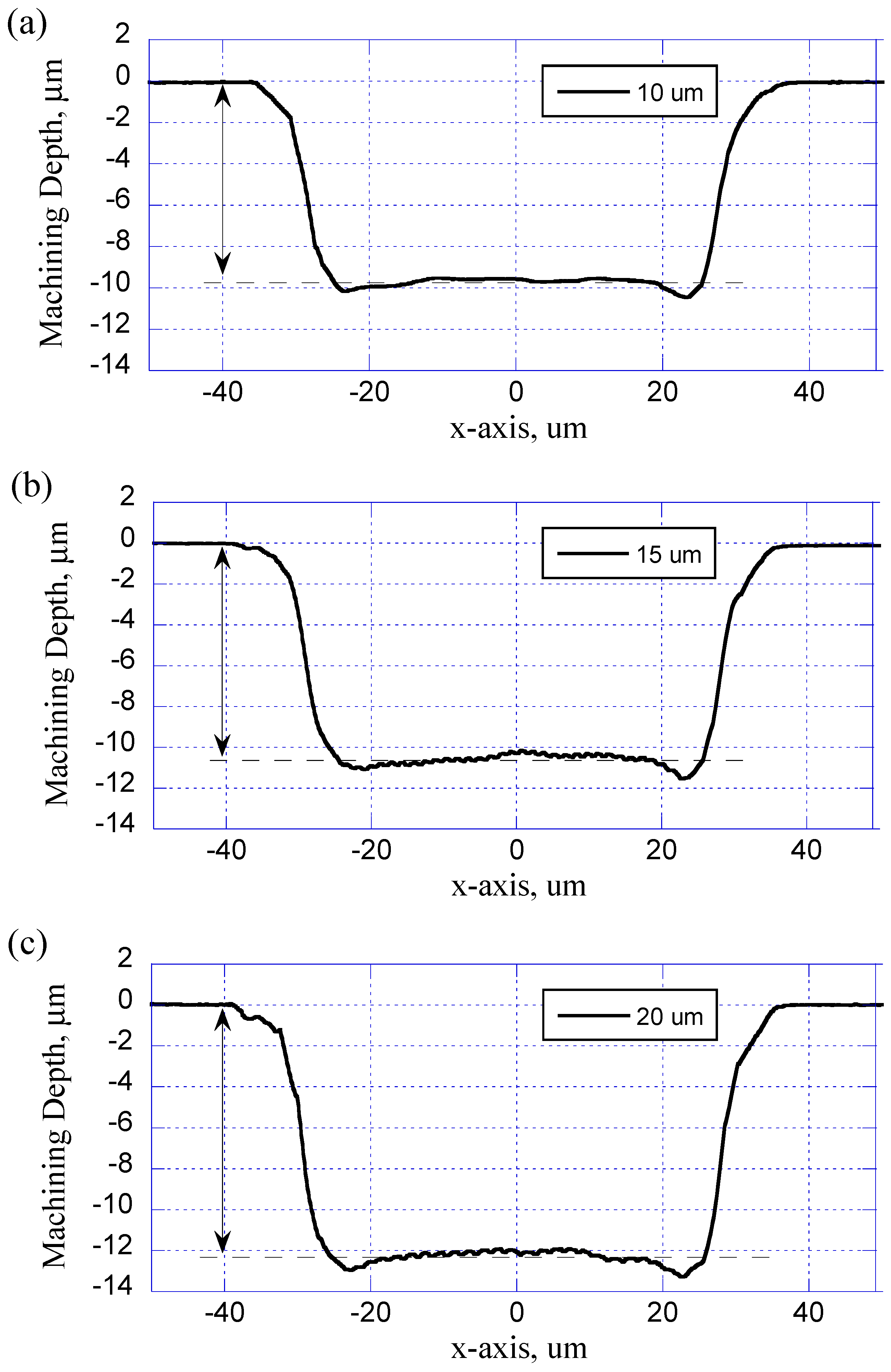
To investigate the effect of the feature size on the optical diffraction phenomenon, mask patterns were designed with three different element sizes (d = 10, 15, and 20 μm) and different values of the hole-radius (r). Each mask pattern had dimensions of 500 × 500 μm2, so the projected machining area on the PC substrate had a size of 50 × 50 μm2 due to the 10× de-magnification factor of the image projection system. Figure 3a–c shows the machined cross-sectional profiles obtained on the PC substrate using mask patterns with element sizes of 10, 15, and 20 μm, respectively, and a constant hole-area opening ratio of 0.65. It is seen that the optical diffraction effect becomes more significant as the feature size of the mask pattern reduces. For example, given an element size of 10 μm, the machined surface profile approaches a flat surface in which the individual features of the arrayed holes can be barely discerned (see Figure 3a). However, for larger element sizes of 15 and 20 μm, periodic machined profiles with periods of 1.5 and 2.0 μm, respectively, are vaguely visible (see Figure 3b,c). In general, the results presented in Figure 3a–c show that the average machined depth decreases as the feature size of the mask pattern reduces even though the hole-area opening ratio remains constant (i.e., 0.65). In other words, it is inferred that the amount of energy rejected by the pupil of the optical imaging system increases with a reducing feature size due to the greater diffraction effect.
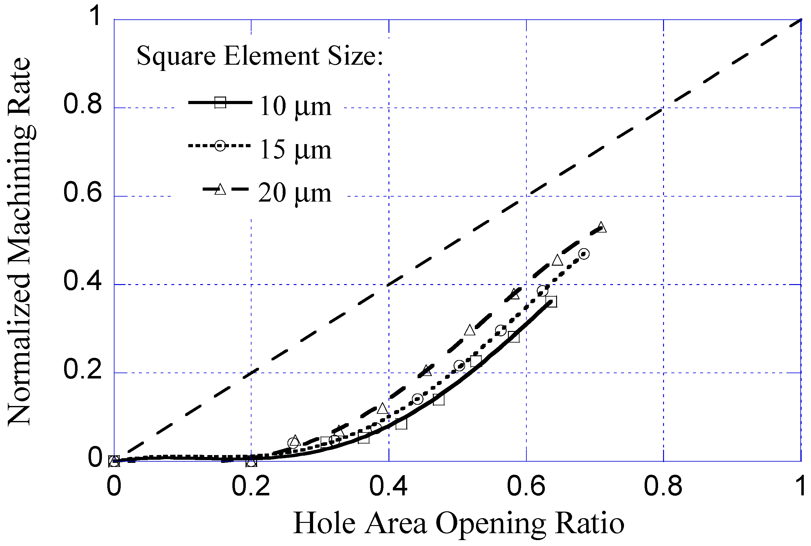
Figure 4 shows the variation of the machining rate with the hole-area opening ratio as a function of the element size. Note that the machining rate is normalized with respect to the basic machining rate obtained in the absence of optical diffraction (i.e., 0.265 μm/pulse). Furthermore, the hole-area opening ratio ranges from 0.2 to 0.7 due to the line-width limitation of the Cr/glass photo-masks preparation system. As expected, the machining rate increases with an increasing hole-area opening ratio. However, the trend is non-linear. This result is reasonable since the projected energy is determined not only by the average optical transmission coefficient (i.e., the hole-area opening ratio) of the photo-mask but also by the optical diffraction effect, which is governed by the feature size of the mask pattern. As can be seen in Figure 4, for a hole-area opening ratio of 0.2, the machining rate is equal to zero, irrespective of the element size. In other words, given a very small hole-area opening ratio, the diffraction effect is so pronounced that the projected energy intensity is below the energy intensity threshold of the PC material. Curve fitting lines for the experimental data obtained with three different elements sizes are displayed in Figure 4. In subsequent works, mask pattern designs will all use a square element size of 10 μm for a stronger optical diffraction effect, achieving smoother energy distribution for better machined surface roughness. The solid fitting line shown in Figure 4 for the case of a 10 μm element size will be used for subsequent mask pattern designs of 3D micromachining.
3. 3D Micromachining Results
Given the experimental results shown in Figure 4, it is possible to inversely derive the hole-arrayed mask pattern required to achieve the desired machining depth of any targeted 3D microstructure. More specifically, the required radius of each and every hole in the mask pattern shown schematically in Figure 2a can be determined by cross-checking the assigned machining depth at the location of each hole with the experimentally determined value of the laser machining rate shown in Figure 4.
The practical feasibility of the proposed excimer 3D laser machining system was evaluated by patterning three different structures on PC substrates, namely conical, trihedral, and pyramidal. In each case, the mask pattern had dimensions of 12 × 12 mm2 (resulting in a 1.2 × 1.2 mm2 machining area). Furthermore, the square element size was set as 10 μm in every case. Finally, the targeted feature size of the machined microstructures was given as 50 μm, corresponding to the base diameter of the conical-shaped microstructure and the baseline lengths of the trihedral and pyramidal microstructures, respectively. For each mask, a square array of microstructures was fabricated with an array pitch of 75 μm. In every case, the structure height and total machining depth were controlled by the number of laser shots fired during the machining process. The laser fluence is 600 mJ/cm2, and 100 pulses are used.
The 3D excimer laser micromachining method proposed here is a subtractive one, so the desired microstructures’ surface profiles are achieved by the variation of machine depth at different position of the sample’s surface. Let h (x, y) be the machining depth at position (x, y) and h (x, y) is pre-determined for each chosen microstructure. To design the hole-opening mask pattern as schematically shown in Figure 2a, we need to determine the hole-opening-area-ratio of each discrete square element, that is, the HR (xi, yj) for the (ith, jth) square element in Figure 2a centering at the coordinates of (xi, yj). The hole-opening-area-ratio of each discrete square element can then be determined by
where is the functional relationship between the normalized machining rate and the hole-area-opening-ratio, as being experimentally determined and shown in Figure 4. Since we are using the 10 μm element size, the solid line with open square symbols in Figure 4 is used. In Equation (1), the is the inverse function of , and is an adjustable constant to cope with the laser fluence and the number of laser shots used in the excimer laser micromachining.
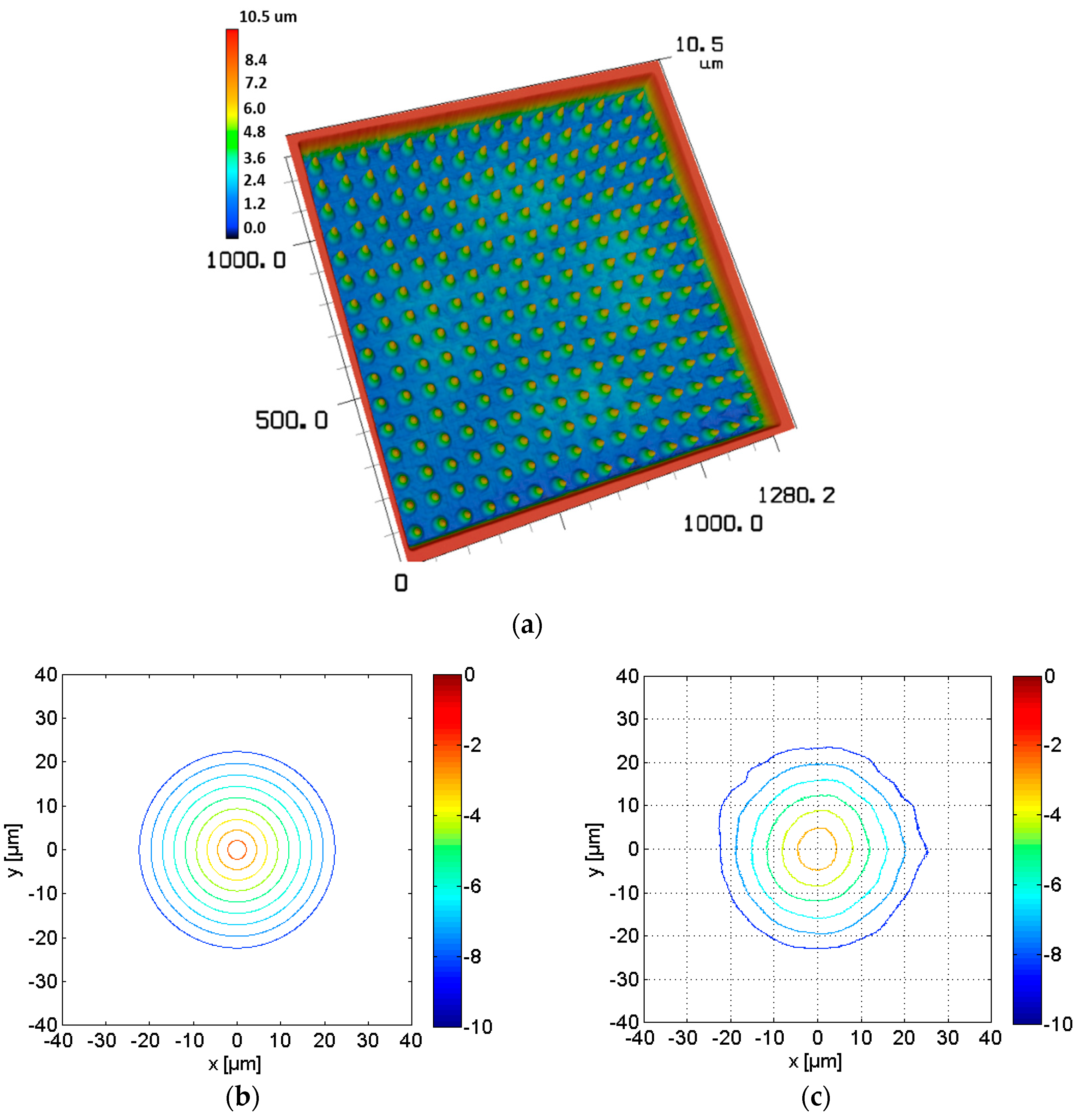
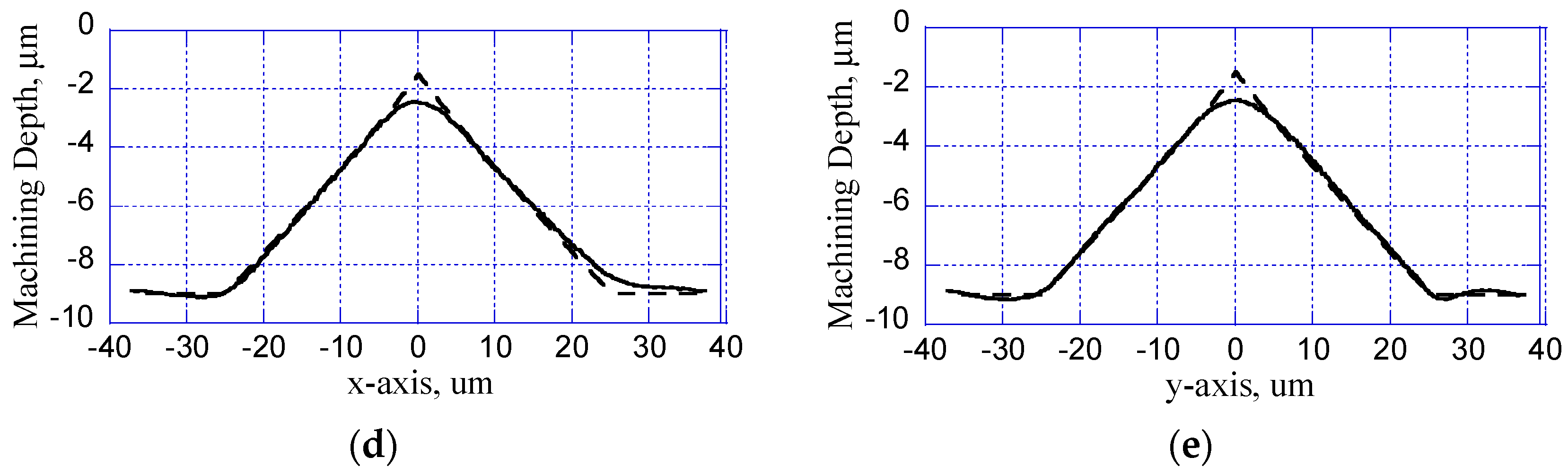
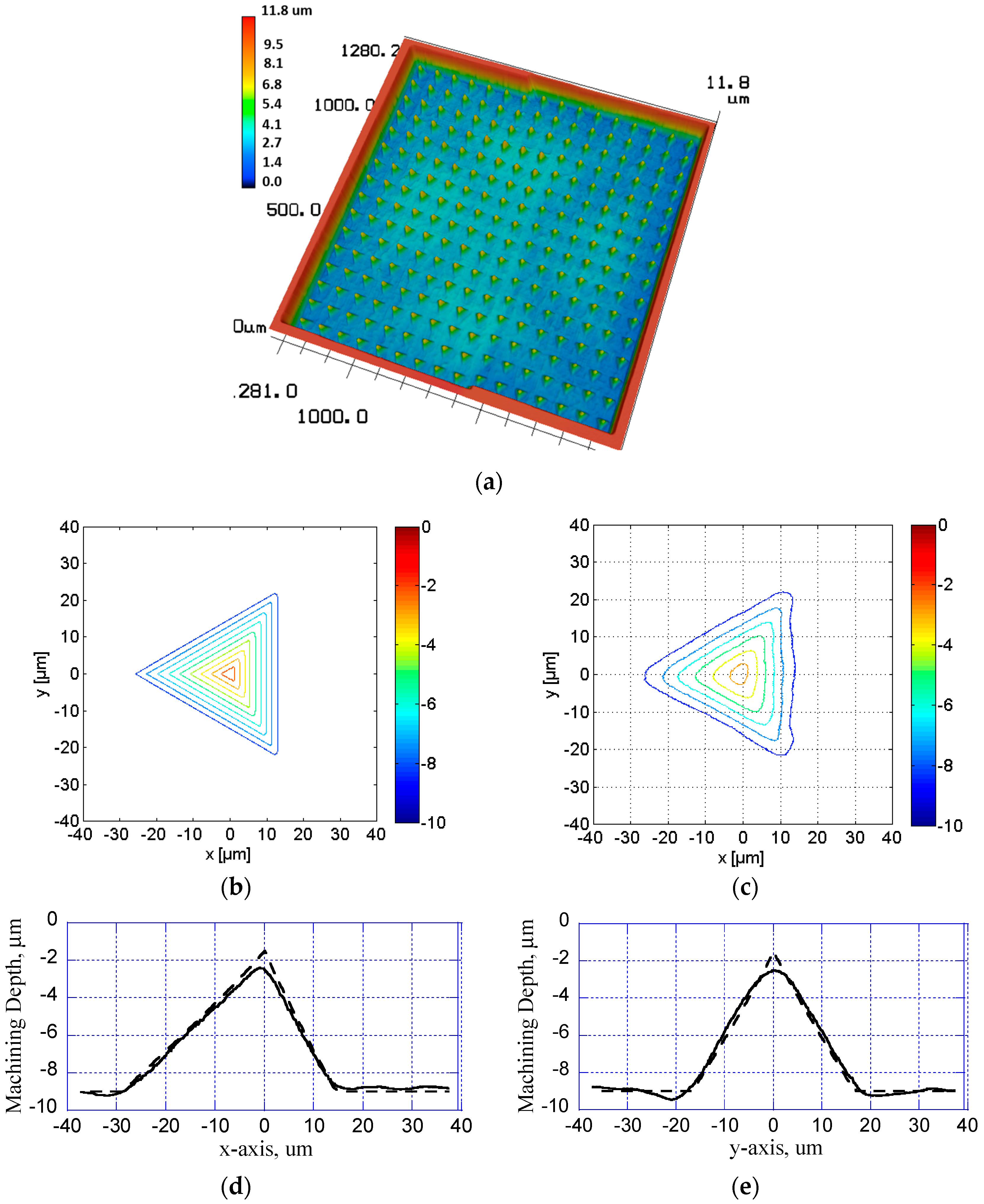
Figure 5, Figure 6 and Figure 7 present the experimental results for the conical, trihedral, and pyramidal microstructures, respectively. Figure 5a, Figure 6a and Figure 7a show the microstructure arrays within the 1.2 × 1.2 mm2 machining areas, while Figure 5b, Figure 6b and Figure 7b show the respective designed machined depth contours. Finally, Figure 5c, Figure 6c and Figure 7c show the actual machined contours of the three microstructures, as measured by a confocal microscope. In Figure 5c,d, it can be seen that the main features of the desired 3D profile are obtained in every case. However, it is noted that the sharp profile features, e.g., points, corners, ridges, and edges, are missing. This finding is reasonable since in the present study, the machining process relies on the optical diffraction effect to achieve the required 3D microstructure profile, so only analog surface profiles can be obtained. Nevertheless, the experimentally obtained microstructures are in good general agreement with the designed profiles. Figure 5d,e, Figure 6d,e and Figure 7d,e compare the measured cross-sectional profiles (solid lines) of the three microstructures along the x- and y-axes, respectively, with the corresponding design profiles (dashed lines). The results confirm the ability of the proposed 3D micromachining system to realize 3D microstructures with a variety of surface profiles and good qualitative agreement with the designed surface contours.
4. Conclusions
This study presents a 3D excimer laser micromachining system in which the required machined profile is obtained by deliberately exploiting the optical diffraction effect. The relationship between the mask pattern feature size and the laser machining rate has been investigated using a hole-array mask pattern. 3D microstructures with conical, trihedral, and pyramidal surface profiles have been fabricated on polycarbonate substrates. It has been shown that the machined profiles are in good qualitative agreement with the designed profiles in every case. The machined microstructures have a characteristic size of approximately 50 μm and have been patterned over a machining area with dimensions of 1.2 × 1.2 mm2. In practice, a larger machining area can be easily achieved by stitching individual machining areas.
The proposed 3D micromachining method has several important advantages over existing excimer laser micromachining systems. For example, since the machining process relies on achieving the optical diffraction effect, the feature size requirement of the hole-array mask pattern is less stringent than that for traditional photo-mask laser machining systems, so the mask can be more easily (i.e., cheaply) made. For the microstructures fabricated in the present study, the minimum line-width requirement for the photo-mask patterns is 2 μm, which is easily obtained using standard industrial practices. Furthermore, the mask pattern design is straightforward since it is necessary only to code the hole-radius into each element according to the required machining depth at the corresponding location on the substrate surface and the known relationship between the laser machining rate and the hole-area opening ratio. Finally, the proposed method provides a versatile technique for creating 3D microstructures with atypical surface profiles and complex pattern arrangements. For example, the conical, trihedral, and pyramidal microstructures shown in Figure 5, Figure 6 and Figure 7 can be arbitrarily mixed within a single machining area by simply re-coding the hole-array mask pattern as required. As a result, the proposed method has significant potential for the realization of a wide range of micro-optics, micro-fluidics, and micro-electro-mechanical-system (MEMS) devices.
Author Contributions
Y.-C.L. conceived and designed the experiments; Y.-H.H. performed the experiments; Y.-H.H. and H.-L.C. analyzed the data; Y.-C.L. and H.-L.C. wrote the paper. All authors have read and approved the final manuscript.
Funding
This research received no external funding.
Conflicts of Interest
The authors declare no conflict of interest.
References
- Dyer, P.E.; Sidhu, J. Excimer laser projection micromachined free-standing polymer films. Opt. Lasers Eng. 1985, 6, 67–77. [Google Scholar] [CrossRef]
- Shukov, G.A.; Smith, A. Micromachining with excimer laser. Lasers Optron 1988, 7, 75–77. [Google Scholar]
- Toenshoff, H.K.; Hesse, D.; Mommsen, J. Micromachining using excimer lasers. CIRP Ann. Manuf. Technol. 1993, 42, 247–251. [Google Scholar] [CrossRef]
- Harvey, E.C.; Rumsby, P.T. Fabrication Techniques and Their Application to Produce Novel Micromachined Structures and Devices Using Excimer Laser Projection. In Proceedings of the SPIE Micromachining and Microfabrication Process Technology III, Austin, TX, USA, 5 September 1997; Volume 3223, pp. 26–33. [Google Scholar]
- Gerlach, K.-H.; Jersch, J.; Dickmann, K.; Hildenhagen, L.J. Design and performance of an excimer-laser based optical system for high precision microstructuring. Opt. Laser Technol. 1997, 29, 439–447. [Google Scholar] [CrossRef]
- Osellame, R.; Cerullo, G.; Ramponi, R. Photonic and Microfluidic Devices in Transparent Materials; Topics in Applied Physics Serias; Springer: Berlin, Germany, 2014. [Google Scholar]
- Zimmer, K.; Hirsch, D.; Bigl, F. Excimer laser machining for the fabrication of analogous microstructures. Appl. Surf. Sci. 1996, 96–98, 425–429. [Google Scholar] [CrossRef]
- Braun, A.; Hoesselbarth, B.; Meinhardt, J.; Bigl, F.; Mehnert, R. Excimer laser micromachining and replication of 3D optical surfaces. Appl. Surf. Sci. 1998, 127–129, 911–914. [Google Scholar] [CrossRef]
- Zimmer, K.; Braun, A.; Bigl, F. Combination of different processing methods for the fabrication of 3D polymer structures by excimer laser machining. Appl. Surf. Sci. 2000, 154, 601–604. [Google Scholar] [CrossRef]
- Braun, A.; Zimmer, K.; Bigl, F. Combination of contour and half-tone masks used in laser ablation. Appl. Surf. Sci. 2000, 168, 178–181. [Google Scholar] [CrossRef]
- Choi, K.H.; Meijer, J.; Masuzawa, T.; Kim, D.-H. Excimer laser micromachining for 3D microstructure. J. Mater. Process. Technol. 2004, 149, 561–566. [Google Scholar] [CrossRef]
- Lee, Y.-C.; Chen, C.-M.; Wu, C.-Y. A new excimer laser micromachining method for 3D microstructures with continuous surface profiles. Sens. Actuators A Phys. 2005, 117, 349–355. [Google Scholar] [CrossRef]
- Lee, Y.-C.; Chen, C.-M.; Wu, C.-Y. Fabrication and characterization of spherical and sspheric microlenses based on excimer laser LIGA-like process. J. Manuf. Sci. Eng. 2007, 129, 126–134. [Google Scholar] [CrossRef]
- Lee, Y.-C.; Wu, C.-Y. Excimer laser micromachining of aspheric microlenses with precise surface profile control and optimal focusing capability. Opt. Lasers Eng. 2007, 45, 116–125. [Google Scholar] [CrossRef]
- Chiu, C.-C.; Lee, Y.-C. Fabricating of aspheric microlens array by excimer laser micromachining. Opt. Lasers Eng. 2011, 49, 1232–1237. [Google Scholar] [CrossRef]
- Chiu, C.-C.; Lee, Y.-C. Excimer laser micromachining of aspheric microlens arrays based on optimal contour mask design and laser dragging method. Opt. Express. 2012, 20, 5922–5935. [Google Scholar] [CrossRef] [PubMed]
- Chiu, C.-C.; Lee, Y.-C. Fabrication of hexagonally arrayed micro-structures with axially symmetrical surface profile by tri-axial excimer laser scanning. Int. J. Mach. Tools Manuf. 2013, 70, 15–21. [Google Scholar] [CrossRef]
- Hayden, C.J. Three-dimensional excimer laser micromachining using greyscale masks. J. Micromech. Microeng. 2003, 13, 599–603. [Google Scholar] [CrossRef]
- Tien, C.-H.; Chien, Y.-E.; Chiu, Y.; Shieh, H.-P. Microlens array fabricated by excimer laser micromachining with gray-tone photolithography. Jpn. J. Appl. Phys. 2003, 42, 1280–1283. [Google Scholar] [CrossRef]
- Holmes, S. Excimer laser micromachining with half-tone masks for the fabrication of 3-D microstructures. IEE Proc. Sci. Meas. Technol. 2004, 151, 85–92. [Google Scholar] [CrossRef]
- Kobayashi, S.; Oka, N.; Watanabe, K.; Ohmori, K.; Inoue, M.; Iguchi, K. Development of Simplified Process for KrF Excimer Half-Tone Mask with Chrome-Shielding Method. In Proceedings of the SPIE 19th Annual Symposium on Photomask Technology, Monterey, CA, USA, 30 December 1999; Volume 3873, pp. 288–296. [Google Scholar]
Figure 1.
A system diagram of an excimer laser micromachining system based on image projection for carrying out both 2D and 3D micromachining.
Figure 1.
A system diagram of an excimer laser micromachining system based on image projection for carrying out both 2D and 3D micromachining.

Figure 2.
(a) Mask pattern design using arrayed square elements with hole-opened apertures. Possible cross-section profiles of machined microstructures at the corresponding position of line (A-A) marked in the mask pattern with (b) negligible, (c) intermediate, and (d) heavy optical diffraction effect during excimer laser machining.


Figure 3.
Laser-machined cross-section profiles using hole-arrayed mask patterns with a hole-area opening ratio of 0.65 and a square element size of (a) 10 µm, (b) 15 µm, and (c) 20 µm.
Figure 3.
Laser-machined cross-section profiles using hole-arrayed mask patterns with a hole-area opening ratio of 0.65 and a square element size of (a) 10 µm, (b) 15 µm, and (c) 20 µm.

Figure 4.
Normalized laser machined rate as a function of hole-area opening ratio when using a hole-arrayed mask patterns with three different square element sizes.
Figure 4.
Normalized laser machined rate as a function of hole-area opening ratio when using a hole-arrayed mask patterns with three different square element sizes.

Figure 5.
Machined conical micro-structures. (a) An overall view of the arrayed microstructures, (b) designed and (c) obtained contours of machined depth, and designed (dash-lines) and machined (solid lines) cross-section profiles along (d) x- and (e) y-axes.
Figure 5.
Machined conical micro-structures. (a) An overall view of the arrayed microstructures, (b) designed and (c) obtained contours of machined depth, and designed (dash-lines) and machined (solid lines) cross-section profiles along (d) x- and (e) y-axes.


Figure 6.
Machined trihedral micro-structures. (a) An overall view of the arrayed microstructures, (b) designed and (c) obtained contours of machined depth, and designed (dash-lines) and machined (solid lines) cross-section profiles along (d) x- and (e) y-axes.
Figure 6.
Machined trihedral micro-structures. (a) An overall view of the arrayed microstructures, (b) designed and (c) obtained contours of machined depth, and designed (dash-lines) and machined (solid lines) cross-section profiles along (d) x- and (e) y-axes.

Figure 7.
Machined pyramidal micro-structures. (a) An overall view of the arrayed microstructures, (b) designed and (c) obtained contours of machined depth, and designed (dash-lines) and machined (solid lines) cross-section profiles along (d) x- and (e) y-axes.
Figure 7.
Machined pyramidal micro-structures. (a) An overall view of the arrayed microstructures, (b) designed and (c) obtained contours of machined depth, and designed (dash-lines) and machined (solid lines) cross-section profiles along (d) x- and (e) y-axes.

© 2018 by the authors. Licensee MDPI, Basel, Switzerland. This article is an open access article distributed under the terms and conditions of the Creative Commons Attribution (CC BY) license (http://creativecommons.org/licenses/by/4.0/).
Share and Cite
MDPI and ACS Style
Hung, Y.-H.; Chien, H.-L.; Lee, Y.-C. Excimer Laser Three-Dimensional Micromachining Based on Image Projection and the Optical Diffraction Effect. Appl. Sci. 2018, 8, 1690. https://0-doi-org.brum.beds.ac.uk/10.3390/app8091690
AMA Style
Hung Y-H, Chien H-L, Lee Y-C. Excimer Laser Three-Dimensional Micromachining Based on Image Projection and the Optical Diffraction Effect. Applied Sciences. 2018; 8(9):1690. https://0-doi-org.brum.beds.ac.uk/10.3390/app8091690
Chicago/Turabian StyleHung, Yu-Hsuan, Hung-Liang Chien, and Yung-Chun Lee. 2018. "Excimer Laser Three-Dimensional Micromachining Based on Image Projection and the Optical Diffraction Effect" Applied Sciences 8, no. 9: 1690. https://0-doi-org.brum.beds.ac.uk/10.3390/app8091690
Note that from the first issue of 2016, this journal uses article numbers instead of page numbers. See further details here.