Post-Sputtering Heat Treatments of Molybdenum on Silicon Wafer
by
 ,
,
Xuguang Jia
1,* ,
,
Ziyun Lin
2,*,
Terry Chien-Jen Yang
2,3,
Binesh Puthen-Veettil
2,4,
Lingfeng Wu
2,
Gavin Conibeer
2 and
Ivan Perez-Wurfl
2 
1
School of Materials Science & Engineering, Jiangsu Collaborative Innovation Center of Photovoltaic Science & Engineering, Jiangsu Province Cultivation Base for State Key Laboratory of Photovoltaic Science and Technology, Changzhou University, Changzhou 213164, China
2
School of Photovoltaic and Renewable Energy Engineering, University of New South Wales, Building H6, Tyree Energy Technologies Building, Kensington, NSW 2052, Australia
3
Now at École Polytechnique Fédérale de Lausanne (EPFL), Institute of Microengineering (IMT), Photovoltaics and Thin-Film Electronics Laboratory, Rue de la Maladière 71b, 2000 Neuchâtel, Switzerland
4
School of Engineering, Macquarie University, Sydney, NSW 2109, Australia
*
Authors to whom correspondence should be addressed.
Appl. Sci. 2018, 8(9), 1692; https://0-doi-org.brum.beds.ac.uk/10.3390/app8091692
Submission received: 2 September 2018
/
Revised: 12 September 2018
/
Accepted: 15 September 2018
/
Published: 18 September 2018
(This article belongs to the Special Issue Next Generation Photovoltaic Solar Cells)
Abstract
:This paper investigated the property evolutions of Mo thin films that were subjected to post-sputtering heat treatments from 700 °C to 1100 °C. It was found that, after annealing, the use of Si wafers eliminated crack formations found in previously reported Mo thin films sputtered on fused silica substrates. The recrystallization of the Mo thin film was found to start at 900 °C, which led to rearrangements of the preferred crystalline orientation and enhancement of grain size when the annealing temperature was further increased. The electrical conductivity of the Mo thin films was majorly affected by the increase of Mo crystallite size as the annealing temperature was increased. Overall, the improvement of material sustainability and compatibility in the high temperature annealing process has made it positive to implement a Mo-Si contact-substrate scheme for vertical structured Si QDs solar cells.
1. Introduction
Vertically structured Si quantum dot (QDs) solar cells implementing a Molybdenum (Mo) back contact layer have been proposed as a method to overcome the current crowding effects found in previous mesa-structured cells [1,2,3,4]. As illustrated in Figure 1a, the drawback of a mesa-structure is the transport of lateral carriers across the thin resistive bottom layer to be collected by the cathode or anode. The resulting low current output has limited the application of this structure towards high efficiency photovoltaic devices as expected. On the contrary, the vertical structure shown in Figure 1b will overcome the current crowding problem by circumventing lateral current flow in the bottom layer. This requires employment of a conductive interlayer between the Si QDs solar cell, and the substrate to serve as the back contact. Apart from the expected improvement in current output, another benefit of the vertical structure is that it simplifies the fabrication process by removing the necessity of reactive ion etching (RIE) to create mesa-islands as previously needed.
Molybdenum (Mo) is selected in this work for the aforementioned back contact interlayer, due to its high melting point and good electrical conductivity. The main investigation on Mo as metal contacts is focused on the effect of the deposition condition in CuInGaSe2 (CIS) based solar cells detailed in previous reports; however, the annealing temperatures were all below 600 due to the limitation imposed by the soda-lime glass substrate used in these studies [5,6,7,8,9,10,11,12]. However, Si QDs formation requires a high temperature annealing process up to 1100 , and thus the Mo thin films should still have good conductivity after such high temperature treatment. Our previous study showed that sputtered Mo thin films on fused silica substrates suffered severe degradation, due to the formation of cracks after annealing at 1100 [3,4]. This was primarily due to the mismatch of the thermal expansion coefficient, which hindered the realization of vertically structured devices. Therefore, in this study, we replaced the fused silica with Si wafers, which have a thermal expansion coefficient close to the value of Mo [4]. Our work discusses the evolution of Mo properties, with respect to different annealing temperatures from 700 to 1100 on Si substrates.
2. Materials and Methods
Si wafers with 500 µm thickness were used as substrates. The deposition of Mo thin film was done in an AJA sputtering system, with a direct current (DC) power of 160 W supplied to the target. The sputtered Mo thin film had a bilayer structure similar to that described in Reference [6], i.e., a 100 nm thick, loosely packed bottom layer (sputtered with Ar flow rate at 30 sccm, and chamber pressure at 15 mTorr), and a 900 nm thick densely packed top layer (sputtered with Ar flow rate at 15 sccm, and chamber pressure at 1.5 mTorr), adding to a total thickness of 1 μm. Annealing of as-sputtered Mo thin films was carried out in a micro-controlled MTI furnace. The quartz tube used to anneal the samples was pre-baked with an N2 flow of 2 LPM at 400 for 1 h, to remove residual contamination and water vapour. The annealing temperature was varied from 700 to 1100 in 100 steps for 1 h, respectively, in an N2 atmosphere. The up/down temperature ramping rate was maintained at 10 /min. In the following discussion, the as-sputtered Mo thin film is denoted as As-Mo, whilst annealed Mo thin films are labelled Mo-Ta, where Ta is the annealing temperature in.
The surface morphology and average roughness of as-sputtered and annealed Mo thin films were examined through a combination of: Atomic force microscopy (AFM) using a Bruker Dimension Icon SPM (Bruker, Bill Clinton, MA, USA), and field emission scanning electron microscopy (FESEM) using a FEI Nova NanoSEM 230 (Thermo Fisher Scientific, Hillsboro, OR, USA). The FESEM was also utilized to check the Mo/Si interface through cross-sectional imaging on the cleaved samples. The evolution of the crystalline structures of Mo thin films was investigated through X-ray diffraction using a PANalytical Xpert Materials Research diffractometer with a Cu Kα source. Finally, the change in electrical properties of Mo thin films, with respect to annealing temperature, which is correlated to the evolution of crystalline properties, was studied based on a 4-point-probe (4PP) measurement using a Jandel Model RM3 setup.
3. Results and Discussion
Figure 2 demonstrates the plan view and cross-sectional scanning of Mo thin films using a combination of AFM and FESEM. The as-sputtered Mo thin film consisted of flake-like grains from, both 3D AFM and plan view FESEM images. These flake-like grains were transformed to stony-like ones upon annealing. Similar changes in morphology with annealing temperature were reported in Reference [10], where the authors attributed the stony-like grains to an association with Mo surface oxidation. From Figure 2c, the thickness of the thin films is around 1 µm and remains unchanged regardless of heat treatments. Mo crystals in the as-sputtered sample had columnar grains along the cross-section of the film, which were packed perpendicular to the Si wafer substrate. With respect to annealing, new interfaces started to form within the grains, and the columnar feature of Mo crystals was lost when the sample was annealed in 900 , which was the recrystallization temperature of Mo [13]. As the annealing temperature increased above 900 , higher energy was obtained in the thin film to facilitate grain boundary migration. As a result, crystals were merged with adjacent grains, and subsequently the enlarged grains grew to a level where their volumes were comparable to the thickness of the film when the sample was annealed at the highest temperature of 1100 . The recrystallization process is usually accompanied by stress relaxation and crystalline texture evolution [14]. The latter effect will manifest as changes in X-ray diffraction (XRD) intensity in particular orientations, which will be discussed in the XRD analysis. Moreover, it is worth noting that no crack formation was identified in any of the samples, which indicated that the application of Si wafer as substrate had overcome the material degradation found in previously fused silica based samples [3,4]. This improvement of material stability with respect to high temperature annealing process, has made Mo-Si promising as a whole for use as contact-substrate for Si QDs solar cells.
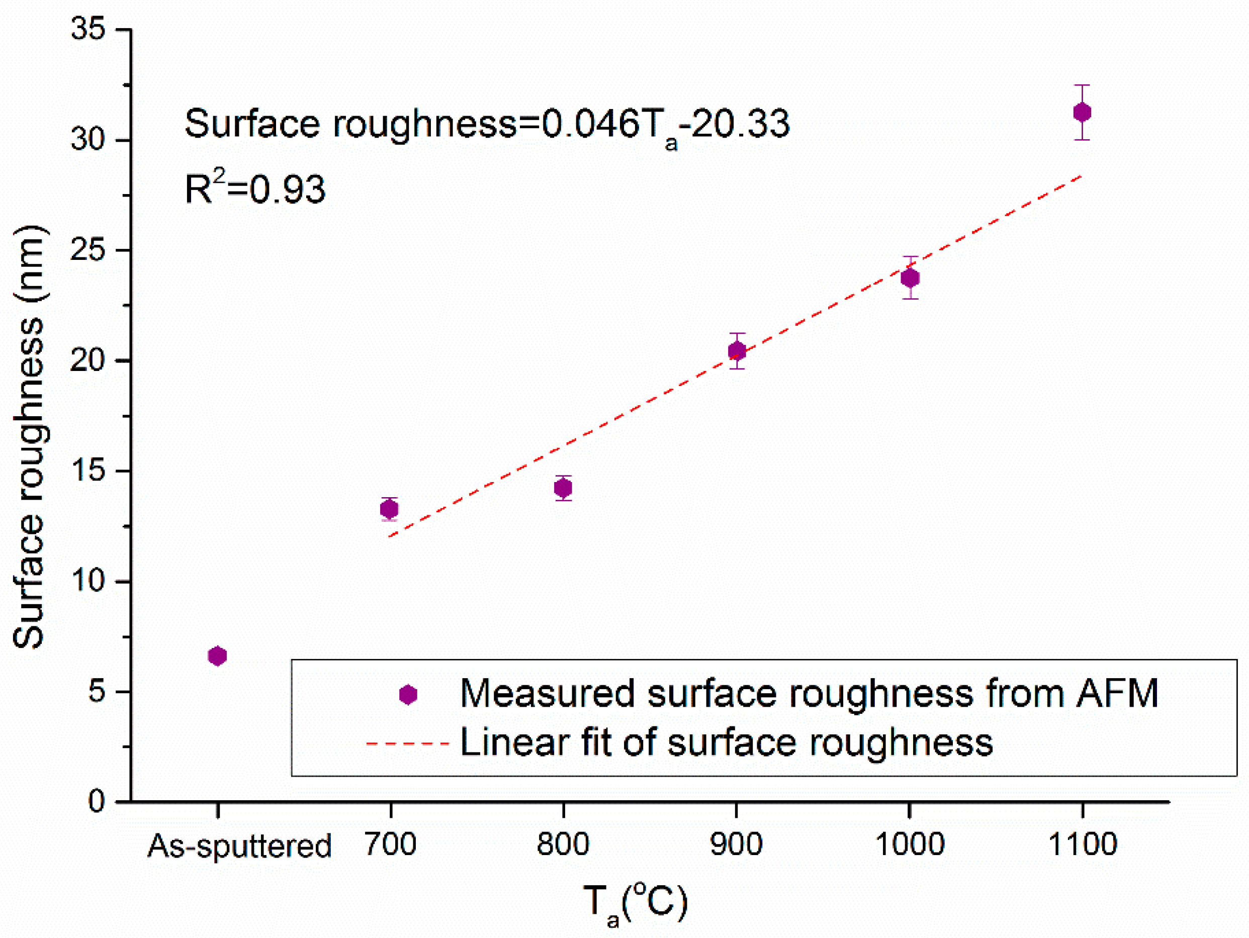
The surface roughness of all samples was determined from AFM measurements on a area, and the results are plotted in Figure 3 as a function of annealing temperature. It was noted that, post-sputtering heat treatments led to rough surfaces on thin films, which increased with annealing temperature following the linear relation indicated in Figure 3. The higher roughness could be explained by the results of larger grain size and formation of Mo oxide defects on the surface, as observed in plan-view FESEM scanning. Even though the maximum roughness obtained on the sample Mo-1100 reached around 30 nm, it is acceptable for fabrication of full Si QDs devices, which are typically 400–500 nm in thickness.
The crystalline properties of Mo thin films, including preferred orientations and crystallite size, were studied via XRD over a range from to , with a step size of . The XRD spectra of each sample in Figure 4 was normalized to its corresponding maximum value. The main peaks identified at around from all samples match the Mo Bragg reflections from (110) and (211) planes, respectively. Weak peaks originated from Mo (200) planes and were also detected on As-Mo, Mo-700, and Mo-800, whilst this peak was hardly noticeable on sample Mo-1000 and Mo-1100. For all annealed samples, XRD peaks related to Mo oxides were identified apart from the Bragg peaks of Mo, which explained the stony-like grains on the FESEM plan views, and the increased surface roughness from AFM. Since no oxide associated peaks were found on the as-sputtered sample, the oxidation of Mo thin films may occur during annealing due to furnace leakage, or after annealing because the sample is still at a fairly high temperature when unloaded from the furnace and cooled down in an ambient environment.
To investigate the degree of Mo crystalline orientation along a certain plane (hkl), the texture coefficient is determined through Equation (1) [9,15]:
where is the number of reflections (i.e., identified Bragg peaks); and are the measured intensity of the (hkl) reflection from the thin film sample, and the intensity of the (hkl) reflection from the corresponding powder sample, respectively, as explained in Reference [15]. A completely randomized sample will have unity values on all planes, whilst values for samples with preferred growth direction will deviate from 1 [15]. To study the preferred orientation of each Mo thin film, the standard deviation of all values compared to randomly orientated samples is determined by Equation (2) [9,15], in which smaller values of correspond to a lesser preferential degree of alignment of the sample. and for each Mo thin film are summarized in Table 1.
As-sputtered Mo and those films annealed below 900 (included) demonstrated strong orientation preference in the (110) direction, since of these samples were at least two times larger than the value for other orientations. On the other hand, the texture coefficient for the (200) plane was the smallest, and the change was marginal for all samples. Moreover, the texture coefficient for the (211) plane first decreased from As-Mo to Mo-800, and then recovered to the level of As-Mo when annealed at 900 . Finally, increased to near 1.5 when the samples were annealed at 1000 and 1100 , respectively. These changes indicated that (110) is the dominant crystalline orientation on as-sputtered Mo thin film, and for samples annealed at 700–900 . However, this preference was lost and shifted to the (211) plane when the annealing temperature was above 900 . From Table 1, the drop in overwhelms the increase in . Therefore the value follows the trend of the , and a peak value of 0.73 was obtained on sample Mo-800. Such changes in texture coefficient and preferred orientation were results of the Mo recrystallization process, as pointed out previously.
Crystallite size of Mo () were estimated using the Scherrer Equation from (110) XRD peaks [16]:
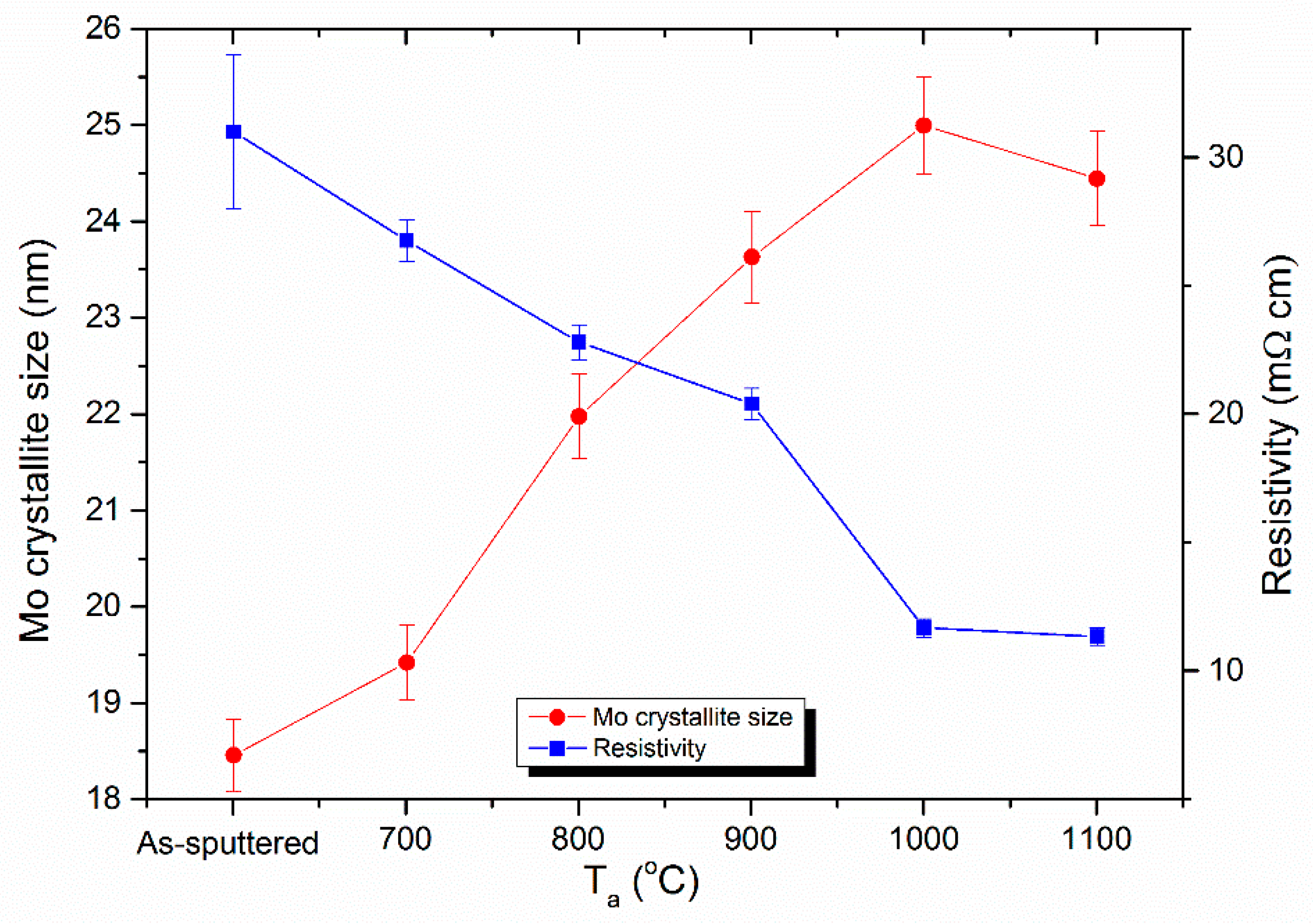
where is the X-ray wavelength of Cu Kα (0.154 nm), is the full width at half maximum (FWHM) of the diffraction peak at a Bragg angle of for the (110) plane. The calculated Mo crystallite sizes from XRD patterns are listed and plotted in Table 1 and Figure 5 (line + solid sphere), respectively. From Table 1, the as-sputtered Mo has an estimated crystallite size of 18.5 nm. Upon annealing, they start to grow in size, almost linearly, with an annealing temperature from 700 to 1000 , see Figure 5. The value finally reaches 24–25 nm and stays relatively unchanged, between samples Mo-1000 and Mo-1100.
The electrical property of Mo thin film was analyzed by examining the sheet resistance of the samples obtained through 4PP measurements. The resistivity of the film was then obtained by dividing the sheet resistance by the thickness of the film (i.e., 1 µm from cross-sectional FESEM). Results of this study are listed in Table 2. The evolution of resistivity as a function of annealing temperature is also plotted in Figure 5 (line + solid square), where the resistivity of Mo thin films reduces with increasing annealing temperature, before it saturates when annealed above 1000 . This trend is obviously opposite to the change in Mo crystallite size on the same plot.
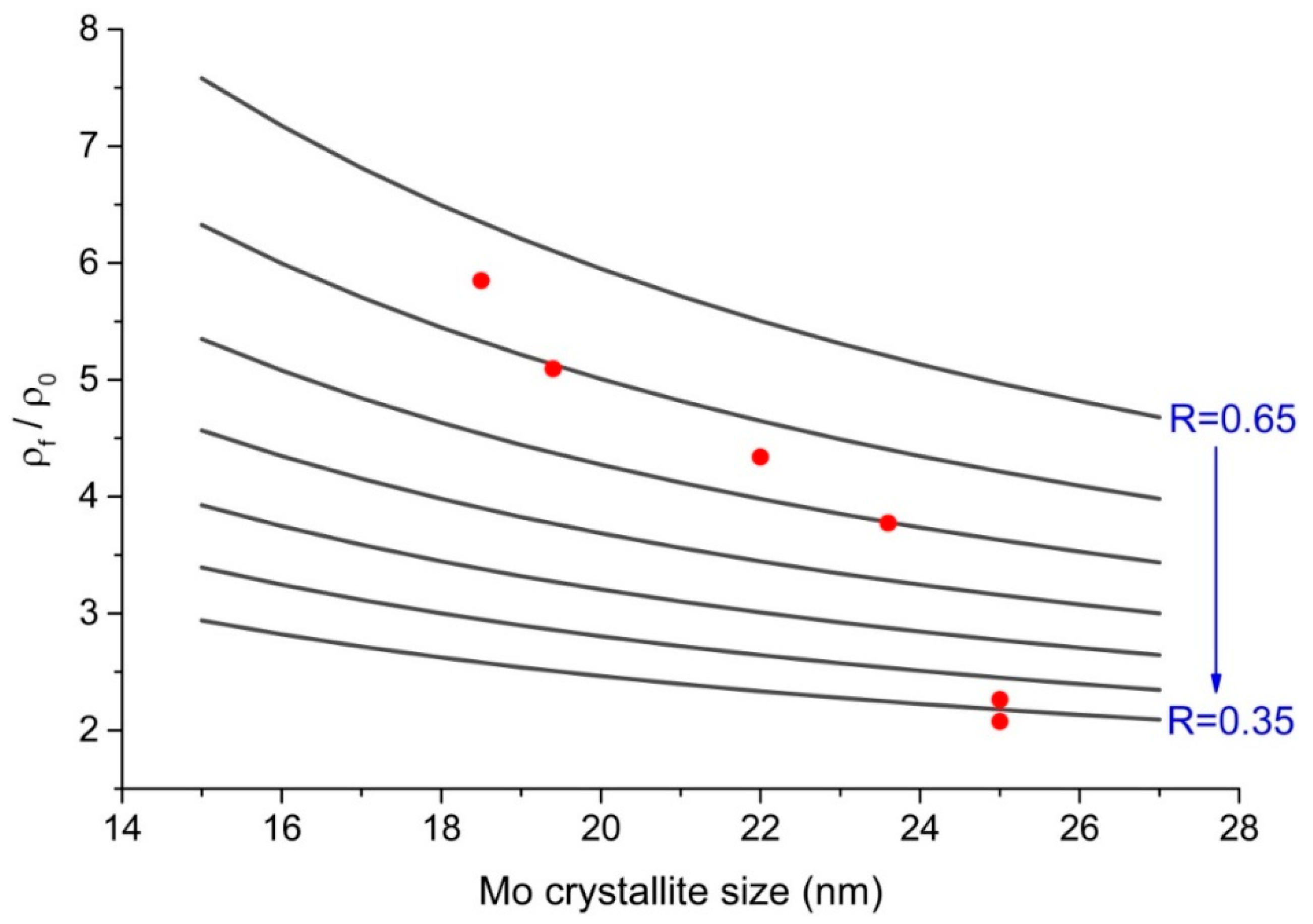
Electrical properties of Mo thin films fabricated in this work were mainly affected by sub-grain boundary electron scatterings and background electron scatterings. At room temperature measurement, the electron mean free path (EMFP) in Mo was 39.5 nm [17,18], which was two orders of magnitude smaller than the thicknesses of Mo thin films in this paper. This made the contribution of external size effect, if at all, to the thin film resistivity due to surface electron scatterings that were insignificant in comparison with background electron scatterings. Therefore, it is safe to assume a unity specular reflection coefficient of [19]. On the contrary, the estimated Mo crystallite sizes from XRD were in the range of 18–25 nm. These values were comparable to the EMFP, and thus the internal size effect of thin film resistivity results from the sub-grain electron scatterings could not be ignored. As a result, the resistivity of Mo thin films can be described using the model established by Mayadas and Shatzkes (MS model) in Equation (4) [19], under the Matthiessen’s rule [20,21].
where and are the resistivity of the thin film and the corresponding single crystal bulk material ( for Mo [17]), respectively. is a factor related to the EMFP at room temperature, the Mo crystallite size in the thin film, and the grain boundary reflection coefficient , following the expression in Equation (5).
The change of ratio as a function of Mo crystallite size is presented in Figure 6, where solid dots are the measurement data, and solid curves are obtained using the MS model in Equation (4) by varying from 0.35 to 0.65, with a step size of 0.05. According to Figure 6, the resistivity of Mo thin films drops when Mo crystallites grow in size, following the trend given by the MS model. This is also consistent with observations from Figure 5, which show that as annealing temperature increases, Mo crystallites are enlarged and hence resistivity is decreased. However, there is no way to fit all experimental data to one theoretical curve [17]. Therefore it can be interpreted within the framework of the MS model, that the value decreased in the range 0.35–0.65 with increased crystallite size [17].
4. Conclusions
This paper studied the properties of Mo thin films sputtered on Si wafer substrates, which were subject to high temperature annealing treatments up to 1100 . The evolutions of surface, interface, and crystalline properties, as a function of annealing temperature were examined. With the replacement of fused-silica by Si wafer as a substrate, crack formations resulting from mismatch of the thermal expansion coefficient were completely eliminated. The recrystallization of the Mo thin film started at 900 , which led to rearrangements of the preferred crystalline orientation, and enhancement of grain size when the annealing temperature was further increased. The electrical conductivity of the Mo thin films was majorly affected by the increase of Mo crystallite size, as the annealing temperature was increased. Overall, the improvement of material sustainability and compatibility in a high temperature annealing process has made it positive to implement a Mo-Si contact-substrate scheme for vertical structured Si QDs solar cells.
Author Contributions
X.J. and Z.L. wrote down the paper and performed the experiments; T.C.-J.Y., B.P.-V, and L.W. analyzed the data and interpreted some results; G. C. and I.P.-W. supervised the findings of this work. All authors discussed the results and contributed to the final manuscript.
Funding
This research received no external funding.
Acknowledgments
This Program has been supported by the Australian Government, through the Australian Renewable Energy Agency (ARENA). Responsibility for the views, information, or advice expressed herein is not accepted by the Australian Government. The authors acknowledge the facilities, and the scientific and technical assistance of the Australian Microscopy & Microanalysis Research Facility at the Electron Microscope Unit at the University of New South Wales, as well as the Australian Centre for Microscopy & Microanalysis at the University of Sydney. The authors would also like to thank Fangyang Liu for his efforts in preparation of sputtered Mo thin films.
Conflicts of Interest
The authors declare that they have no conflict of interest.
References
- Perez-Wurfl, I.; Hao, X.; Gentle, A.; Kim, D.-H.; Conibeer, G.; Green, M.A. Si nanocrystal p-i-n diodes fabricated on quartz substrates for third generation solar cell applications. Appl. Phys. Lett. 2009, 95, 153506. [Google Scholar] [CrossRef]
- Di, D.; Perez-Wurfl, I.; Gentle, A.; Kim, D.-H.; Hao, X.; Shi, L.; Conibeer, G.; Green, M.A. Impacts of post-metallisation processes on the electrical and photovoltaic properties of si quantum dot solar cells. Nanoscale Res. Lett. 2010, 5, 1762–1767. [Google Scholar] [CrossRef] [PubMed]
- Lin, Z.; Perez-Wurfl, I.; Wu, L.; Jia, X.; Zhang, T.; Puthen-Veettil, B.; Zhang, H.; Di, D.; Conibeer, G. Investigation in feasibility of molybdenum as a back contact layer for silicon based quantum dot solar cells. In Proceedings of the SPIE 8620, Physics, Simulation, and Photonic Engineering of Photovoltaic Devices II, San Francisco, CA, USA, 25 March 2013; pp. 86201W–86207W. [Google Scholar]
- Lin, Z.; Wu, L.; Jia, X.; Zhang, T.; Puthen-Veettil, B.; Yang, T.C.-J.; Conibeer, G.; Perez-Wurfl, I. Boron doped Si rich oxide/SiO2 and silicon rich nitride/sinx bilayers on molybdenum-fused silica substrates for vertically structured si quantum dot solar cells. J. Appl. Phys. 2015, 118, 045303. [Google Scholar] [CrossRef]
- Repins, I.; Contreras, M.A.; Egaas, B.; DeHart, C.; Scharf, J.; Perkins, C.L.; To, B.; Noufi, R. 19·9%-efficient Zno/Cds/CuInGaSe2 solar cell with 81·2% fill factor. Prog. Photovolt. Res. Appl. 2008, 16, 235–239. [Google Scholar] [CrossRef]
- Scofield, J.H.; Duda, A.; Albin, D.; Ballard, B.L.; Predecki, P.K. Sputtered molybdenum bilayer back contact for copper indium diselenide-based polycrystalline thin-film solar cells. Thin Solid Films 1995, 260, 26–31. [Google Scholar] [CrossRef]
- Guillén, C.; Herrero, J. Low-resistivity mo thin films prepared by evaporation onto 30 cm × 30 cm glass substrates. J. Mater. Process. Technol. 2003, 143–144, 144–147. [Google Scholar] [CrossRef]
- Gordillo, G.; Grizález, M.; Hernandez, L.C. Structural and electrical properties of DC sputtered molybdenum films. Solar Energy Mater. Sol. Cells 1998, 51, 327–337. [Google Scholar] [CrossRef]
- Zoppi, G.; Beattie, N.; Major, J.; Miles, R.; Forbes, I. Electrical, morphological and structural properties of rf magnetron sputtered mo thin films for application in thin film photovoltaic solar cells. J. Mater. Sci. 2011, 46, 4913–4921. [Google Scholar] [CrossRef]
- Chelvanathan, P.; Zakaria, Z.; Yusoff, Y.; Akhtaruzzaman, M.; Alam, M.M.; Alghoul, M.A.; Sopian, K.; Amin, N. Annealing effect in structural and electrical properties of sputtered mo thin film. Appl. Surf. Sci. 2015, 334, 129–137. [Google Scholar] [CrossRef]
- Tong, J.; Luo, H.-L.; Xu, Z.-A.; Zeng, H.; Xiao, X.-D.; Yang, C.-L. The effect of thermal annealing of mo film on the cuinse2 layer texture and device performance. Sol. Energy Mater. Sol. Cells 2013, 119, 190–195. [Google Scholar] [CrossRef]
- Scragg, J.J.; Ericson, T.; Fontané, X.; Izquierdo-Roca, V.; Pérez-Rodríguez, A.; Kubart, T.; Edoff, M.; Platzer-Björkman, C. Rapid annealing of reactively sputtered precursors for Cu2ZnSns4 solar cells. Prog. Photovolt. Res. Appl. 2014, 22, 10–17. [Google Scholar] [CrossRef]
- Committee, A.I.H. Properties and Selection: Nonferrous Alloys and Special-Purpose Materials, 10th ed.; ASM International: Kinsman Road Materials Park, OH, USA, 1990; p. 575. [Google Scholar]
- Lee, D.N. Strain energy release maximization model for evolution of recrystallization textures. Int. J. Mech. Sci. 2000, 42, 1645–1678. [Google Scholar] [CrossRef]
- Kim, K.H.; Chun, J.S. X-ray studies of SnO2 prepared by chemical vapour deposition. Thin Solid Films 1986, 141, 287–295. [Google Scholar] [CrossRef]
- Hasegawa, S.; Watanabe, S.; Inokuma, T.; Kurata, Y. Structure and grain boundary defects of recrystallized silicon films prepared from amorphus silicon deposited using disilane. J. Appl. Phys. 1995, 77, 1938–1947. [Google Scholar] [CrossRef]
- Vávra, I.; Luby, Š. Resistivity and structure of evaporated polycrystalline molybdenum films. Thin Solid Films 1980, 69, 169–173. [Google Scholar] [CrossRef]
- Fawcett, E.; Griffiths, D. The fermi surface areas of chromium, molybdenum and tungsten. J. Phys. Chem. Solids 1962, 23, 1631–1635. [Google Scholar] [CrossRef]
- Mayadas, A.; Shatzkes, M.; Janak, J. Electrical resistivity model for polycrystalline films: The case of specular reflection at external surfaces. Appl. Phys. Lett. 1969, 14, 345–347. [Google Scholar] [CrossRef]
- Leonard, W.F.; Lin, S.F. The validity of matthiessen’s rule for metallic films. Thin Solid Films 1975, 28, L9–L12. [Google Scholar] [CrossRef]
- Philipp, M. Electrical Transport and Scattering Mechanisms in Thin Silver Films for Thermally Insulating Glazing. 2011. Available online: http://tud.qucosa.de/landing-page/?tx_dlf[id]=http%3A%2F%2Ftud.qucosa.de%2Fapi%2Fqucosa%253A24607%2Fmets (accessed on 1 August 2018).
Figure 1.
Schematic diagram of (a) mesa-structured and (b) vertical structured Si quantum dot (QDs) solar cells (not to scale). Current flows are also indicated.
Figure 1.
Schematic diagram of (a) mesa-structured and (b) vertical structured Si quantum dot (QDs) solar cells (not to scale). Current flows are also indicated.

Figure 2.
(a) 3D Atomic force microscopy (AFM) images, (b) field emission scanning electron microscopy (FESEM) plan views, and (c) FESEM cross-sectional views of Mo thin films as a function of annealing temperature.
Figure 2.
(a) 3D Atomic force microscopy (AFM) images, (b) field emission scanning electron microscopy (FESEM) plan views, and (c) FESEM cross-sectional views of Mo thin films as a function of annealing temperature.


Figure 3.
Surface roughness of Mo thin films, as a function of annealing temperature. Linear fit of measurement data from 700 to 1100 is also demonstrated.
Figure 3.
Surface roughness of Mo thin films, as a function of annealing temperature. Linear fit of measurement data from 700 to 1100 is also demonstrated.

Figure 4.
X-ray diffraction (XRD) patterns of Mo thin films, as a function of annealing temperature. Mo Bragg peaks originating from (110), (200), and (211) planes are labelled with dotted lines for guides to the eye. Other unlabeled peaks are associated with Mo oxides phases.
Figure 4.
X-ray diffraction (XRD) patterns of Mo thin films, as a function of annealing temperature. Mo Bragg peaks originating from (110), (200), and (211) planes are labelled with dotted lines for guides to the eye. Other unlabeled peaks are associated with Mo oxides phases.

Figure 5.
Evolution of Mo crystallite size and resistivity of Mo thin films, as a function of annealing temperature.
Figure 5.
Evolution of Mo crystallite size and resistivity of Mo thin films, as a function of annealing temperature.

Figure 6.
Change of as a function of Mo crystallite size. Solid dots are measurement data, and solid curves are calculated using Equations (4) and (5), with value varies from 0.65 to 0.35, with a step of 0.05.
Figure 6.
Change of as a function of Mo crystallite size. Solid dots are measurement data, and solid curves are calculated using Equations (4) and (5), with value varies from 0.65 to 0.35, with a step of 0.05.


Table 1.
Summary of texture coefficient, preferred orientation, (110) full width at half maximum (FWHM), and crystallite size, calculated from the (110) peak of Mo thin films, as a function of annealing temperature.
Table 1.
Summary of texture coefficient, preferred orientation, (110) full width at half maximum (FWHM), and crystallite size, calculated from the (110) peak of Mo thin films, as a function of annealing temperature.
| Sample | (110) FWHM () | Crystallite Size from (110) (nm) | ||||
|---|---|---|---|---|---|---|
| As-Mo | 2.24 | 0.04 | 1.02 | 0.59 | 0.459 | 18.5 |
| Mo-700 | 2.41 | 0.05 | 0.97 | 0.64 | 0.436 | 19.4 |
| Mo-800 | 2.69 | 0.06 | 0.87 | 0.73 | 0.385 | 22.0 |
| Mo-900 | 2.46 | 0.00 | 1.04 | 0.67 | 0.358 | 23.6 |
| Mo-1000 | 0.56 | 0.00 | 1.47 | 0.45 | 0.339 | 25.0 |
| Mo-1100 | 0.58 | 0.00 | 1.46 | 0.45 | 0.3464 | 25.0 |
Table 2.
Summary of sheet resistance and resistivity of Mo thin films, as a function of annealing temperature.
Table 2.
Summary of sheet resistance and resistivity of Mo thin films, as a function of annealing temperature.
| Sample | Sheet Resistance (mΩ/□) | Resistivity (µΩ cm) |
|---|---|---|
| As-Mo | 310.1 | 31 |
| Mo-700 | 267.4 | 27 |
| Mo-800 | 227.5 | 23 |
| Mo-900 | 204.3 | 20 |
| Mo-1000 | 116.6 | 12 |
| Mo-1100 | 113.5 | 11 |
© 2018 by the authors. Licensee MDPI, Basel, Switzerland. This article is an open access article distributed under the terms and conditions of the Creative Commons Attribution (CC BY) license (http://creativecommons.org/licenses/by/4.0/).
Share and Cite
MDPI and ACS Style
Jia, X.; Lin, Z.; Yang, T.C.-J.; Puthen-Veettil, B.; Wu, L.; Conibeer, G.; Perez-Wurfl, I. Post-Sputtering Heat Treatments of Molybdenum on Silicon Wafer. Appl. Sci. 2018, 8, 1692. https://0-doi-org.brum.beds.ac.uk/10.3390/app8091692
AMA Style
Jia X, Lin Z, Yang TC-J, Puthen-Veettil B, Wu L, Conibeer G, Perez-Wurfl I. Post-Sputtering Heat Treatments of Molybdenum on Silicon Wafer. Applied Sciences. 2018; 8(9):1692. https://0-doi-org.brum.beds.ac.uk/10.3390/app8091692
Chicago/Turabian StyleJia, Xuguang, Ziyun Lin, Terry Chien-Jen Yang, Binesh Puthen-Veettil, Lingfeng Wu, Gavin Conibeer, and Ivan Perez-Wurfl. 2018. "Post-Sputtering Heat Treatments of Molybdenum on Silicon Wafer" Applied Sciences 8, no. 9: 1692. https://0-doi-org.brum.beds.ac.uk/10.3390/app8091692
Note that from the first issue of 2016, this journal uses article numbers instead of page numbers. See further details here.