Article

A Virtual Impedance Control Strategy for Improving the Stability and Dynamic Performance of VSC–HVDC Operation in Bidirectional Power Flow Mode

School of Electrical Engineering and Automation, Wuhan University, Wuhan 430072, China
*
Author to whom correspondence should be addressed.
Submission received: 19 July 2019 / Revised: 31 July 2019 / Accepted: 1 August 2019 / Published: 5 August 2019
(This article belongs to the Special Issue HVDC for Grid Services in Electric Power Systems)

Abstract

:
It is a common practice that one converter controls DC voltage and the other controls power in two-terminal voltage source converter (VSC)–based high voltage DC (HVDC) systems for AC gird interconnection. The maximum transmission power from a DC-voltage-controlled converter to a power-controlled converter is less than that of the opposite transmission direction. In order to increase the transmission power from a DC-voltage-controlled converter to a power-controlled converter, an improved virtual impedance control strategy is proposed in this paper. Based on the proposed control strategy, the DC impedance model of the VSC–HVDC system is built, including the output impedance of two converters and DC cable impedance. The stability of the system with an improved virtual impedance control is analyzed in Nyquist stability criterion. The proposed control strategy can improve the transmission capacity of the system by changing the DC output impedance of the DC voltage-controlled converter. The effectiveness of the proposed control strategy is verified by simulation. The simulation results show that the proposed control strategy has better dynamic performance than traditional control strategies.

1. Introduction

With the development of power electronic devices, VSC–HVDC systems have been widely applied to AC grid interconnection because of their independent decoupling control of active and reactive power [1,2,3]. Recently, a large number of studies on modeling, control, and stability analysis of VSC–HVDC system have been published [4,5,6,7,8,9,10]. Previous studies have shown that the interaction between converters or between the converter and the grid influences the stability of a system. DC- side oscillation is a problem in VSC–HVDC and has been reported in a real project [11]. When DC side oscillation occurs, a DC system will not work and will impact on the power system. Therefore, the DC-side stability of VSC–HVDC should be evaluated before connecting it to the main grid.
In VSC–HVDC systems applied to AC grid interconnection, active power often needs bidirectional transmission [12]. However, studies show that the maximum transmission power of the DC-voltage-controlled converter to power-controlled converter is less than that in the opposite power flow direction [13]. An Impedance-based approach can be adopted to analyze the influence of VSC–HVDC systems with different directions of transmission power on stability [13].
The impedance stability criterion was proposed in [14] and used in grid-connected inverters [15]. It was applied as a stability criterion in a VSC–HVDC system [12,16,17,18,19]. The impedance model of two-terminal VSC–HVDCs was built in [12], and the cause of DC current resonance was analyzed with Nyquist stability criteria. Different subsystems were selected to analyze the DC-side stability of the VSC–HVDC system with a transfer function method in [16]. The influence of overhead transmission lines, DC cables, and the DC-side filter on system stability was investigated in [17]. The different performances of the lumped parameter and distributed parameter circuit models in stability analysis were discussed in [18]. It was found that the distributed parameter circuit model is more accurate in stability analysis.
In the condition of VSC–HVDC for AC Grid interconnection, the maximum transmission capacities of the different power flow directions are different. Thus, a control strategy is required to improve the transmission capacity from the DC-voltage-controlled converter to the power-controlled converter to improve resource utilization efficiency. To increase the maximum transmission power, the DC side oscillation must be suppressed. The suppression methods of DC side oscillation can be classified into passive methods [20,21] and active methods [22,23,24,25,26,27,28,29]. Passive methods suppress resonance by introducing a passive damper branch into the circuit to remodel the impedance of the source converter or load converter in a cascaded system. Active methods suppress resonance by introducing voltage and current feedback control in a controller to improve the impedance of the source converter or load converter. Virtual impedance is widely used in control systems as an active damping control method [24,25,26,27,28,29]. It can be introduced to suppress DC-side oscillation [24,25], to limit output current for voltage controlled inverters during overloads or faults [26,27], to improve the stability of a grid-connected inverter by change its input admittance [28], and to enhance the small-signal stability of a modular multilevel converter (MMC) based DC grid [29].
Virtual impedance in the DC voltage control loop can suppress the DC-side oscillation of a VSC–HVDC transmission system and improve its stability margin and the transmission capacity of the system [24,25]. However, virtual impedance control leads to steady-state errors in the DC output voltage of DC-voltage-controlled converters, due to different operating points [25]. An improved virtual impedance control strategy is proposed in this paper. To design an appropriate control strategy, a stability analysis is required. Thus, a DC impedance-based model of VSC–HVDC is built, and the stability of the system is analyzed based on impedance stability criteria.
The rest of the paper is organized as follows: Section 2 describes the system’s structure and the simulation of a VSC–HVDC system, as well as the design of an improved virtual impedance control. Section 3 presents the impedance model of an HVDC system. Section 4 conducts a stability analysis on the basis of impedance stability criteria, and Section 5 shows the simulation verification. Section 6 summarizes the proposed method.

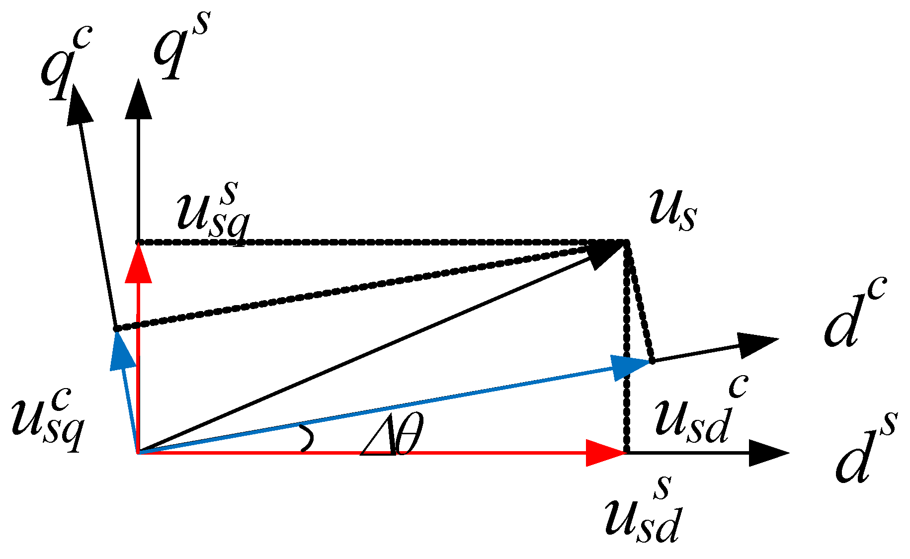
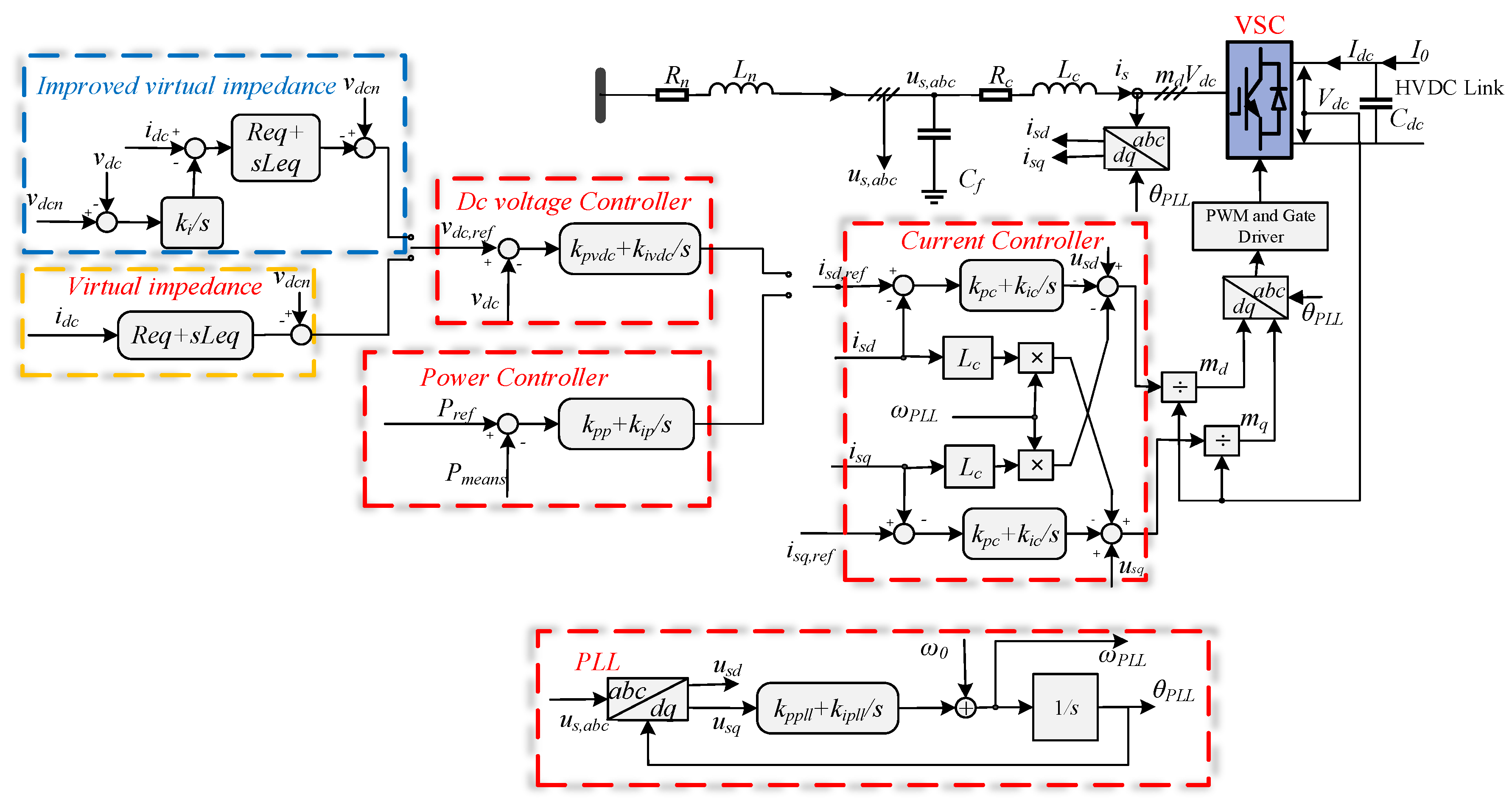
2. Improved Virtual Impedance Control Principle

This paper mainly studies a two-level topology structure. The analysis in this paper can be also applicable to an MMC system if the dc bus voltage ripples are insignificant [12]. A two-level VSC–HVDC system used in AC grid interconnection is depicted in Figure 1. Figure 1 shows a DC voltage-controlled converter and a power-controlled converter on the left and right sides, respectively. The two converters have an identical structure. Rn1 + jXn1 and Rn2 + jXn2 are the equivalent impedance of the AC system, Rc1 + 1L1 and Rc2 + 2Lc2 are the impedance of the filter reactor, Cf1 and Cf2 are the filter capacitors, m · 1 and m 2 · are the modulations of the converter station, u · s 1 and u · s 2 are the AC voltage at point of common coupling, u · g 1 and u · g 2 are the AC voltage of the AC system, i · s 1 and i · s 2 are the AC current flowing through the filter reactor, and i · g 1 and i · g 2 are the AC current flowing through the AC system. The DC cable is a π type, with an equivalent resistance of Rd, an equivalent inductance of Ld, and an equivalent capacitance of Cd.
The modeling and control of the VSC–HVDC system are presented in a synchronous rotating frame (SRF). The transformation of the three-phase quantity from stationary reference frame to the SRF is based on the amplitude-invariant Park transformation, with the d-axis aligned with the voltage vector us and q-axis leading the d-axis by 90°. The grid voltage defines the system’s dq reference. A phase-locked loop (PLL) defines the controller dq reference. The system reference is aligned with the PLL reference in a steady state. When a small disturbance occurs, the system reference is no longer aligned with the PLL reference. The relationship between the system reference and the PLL reference under a small disturbance is shown in Figure 2.
Here, subscript dq represent the components of the physical quantity in the SRF. Subscript 0 represents the value of the physical quantity at the static working point, subscript ref represents the given value of physical quantity, and subscript Δ represents the small disturbance components of the physical quantity. Superscript c represents the components of physical quantity in the PLL reference, and superscript s represents the components in the system reference.
The simulation model of VSC–HVDC in Figure 1 is built on a MATLAB/Simulink. The system parameters are shown in the following table. The vector current control [13] is adopted in the two converters, and the control is shown in Figure 3. For symmetry of the VSC–HVDC system, subscripts 1,2 of the system parameters in Table 1 and the control diagram in Figure 3 are omitted. In the model, controller parameters are per unit. The base angular grid frequency is 50 Hz, the base grid voltage is 110 kV, the base system capacity is 500 MW, and the base DC voltage is 250 kV. According to the parameters in Table 1, the system’s closed-loop bandwidth with a DC voltage controller is 65 Hz, and the system’s open-loop phase margin is 58 degrees. The system’s closed-loop bandwidth with an active power controller is 8 Hz, and the system’s open-loop phase margin is 150 degrees. The system’s closed-loop bandwidth with the current controller is 180 Hz, and the system’s open-loop phase margin is 85 degrees.
The power flow direction from the power-controlled converter to the DC voltage-controlled converter is set to positive. Figure 4 shows the resulting time-domain responses of the DC voltage of the VSC–HVDC system. At 2 s, the active power instruction value steps from 500 MW to −500 MW, and the length of the DC cable is 50 km. It can be observed that the DC voltage starts to oscillate, the active power starts to fluctuate, and the system loses stability.
The power-controlled converter exhibits a constant power load (CPL) when the active power is transmitted from the DC-voltage controlled converter to the power-controlled converter. The incremental input resistance characteristic caused by CPL affects the stability of the VSC–HVDC system [24].
A virtual impedance control strategy is introduced in the DC-voltage-controlled converter to mitigate the DC-side oscillation caused by the negative incremental input resistance characteristic of the power-controlled converter. The expression of the virtual impedance control is
v d c r e f = v d c n ( R e q + s L e q ) i d c
where vdcref is the DC voltage reference value, vdcn is the no-load DC voltage of the converter, and Req and Leq are the set values for the virtual impedance. Due to the addition of current feedback, under loaded conditions, there will be a fixed steady-state error between the DC voltage reference value and the measured value, which almost equals R e q i d c . Thus, the steady-state error increases with an increase in the transmission power (in both power flow directions).
In order to eliminate the steady-state error caused by virtual impedance, this paper modifies the voltage control loop, as shown by the blue dotted line frame in Figure 5.
i d c n = k i s ( v d c n v d c )
v d c r e f = v d c n ( R e q + s L e q ) ( i d c i d c n )

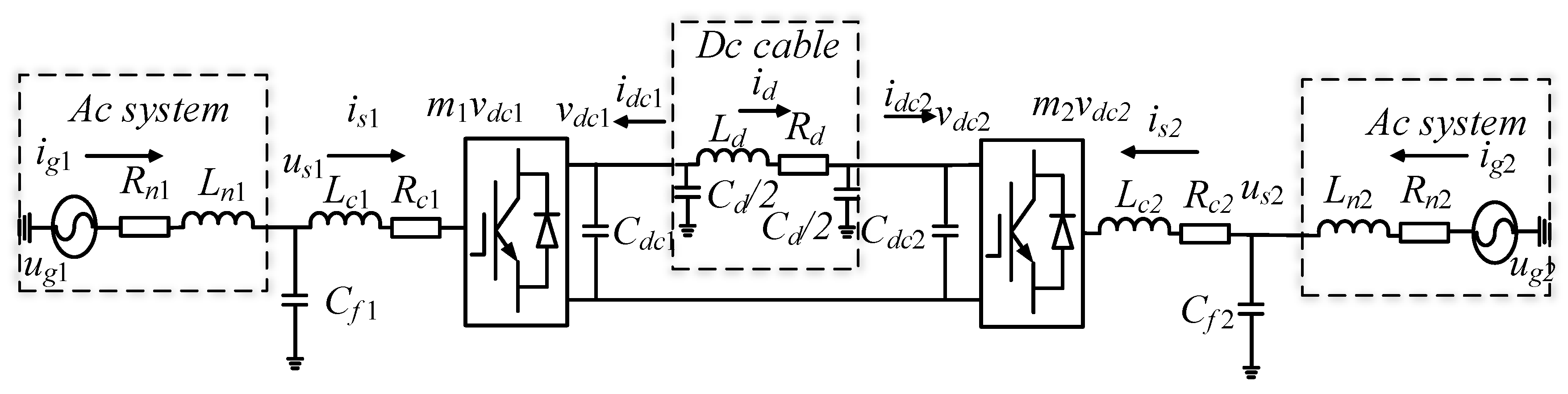
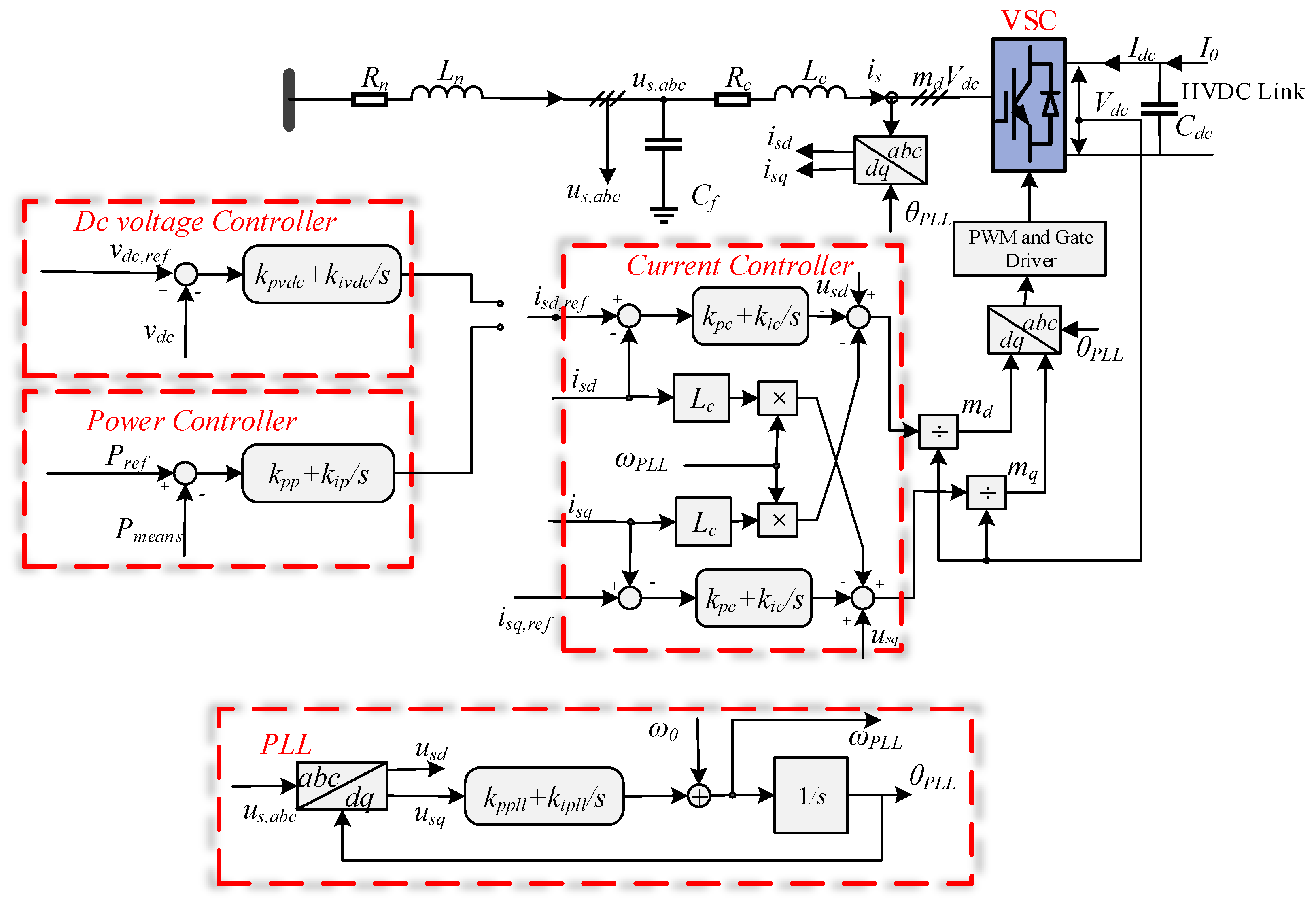
3. Impedance Model of Converters with Improved Virtual Impedance Control Strategy

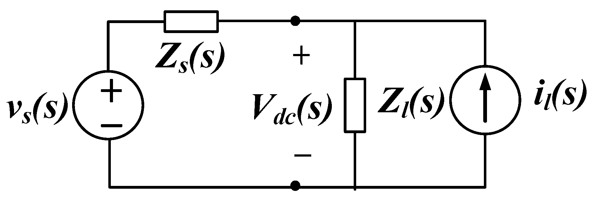
3.1. DC-Side Impedance Modeling of DC-Voltage-Controlled Converter

The linearized dynamic equations of the DC voltage-controlled converter are expressed as
[ m d 0 m q 0 ] Δ v d c + v d c 0 [ Δ m d s Δ m q s ] + Z 0 ( s ) [ Δ i s d s Δ i s q s ] = [ Δ u s d s Δ u s q s ]
[ Δ u s d s Δ u s q s ] = Z g ( s ) [ Δ i g d s Δ i g q s ]
[ Δ i g d s Δ i g q s ] = [ Δ i s d s Δ i s q s ] + Y c f ( s ) [ Δ u s d s Δ u s q s ]
where
Z 0 = [ R c + s L c ω 0 L c ω 0 L c R c + s L c ]
Z g = [ R n + s L n ω 0 L n ω 0 L n R n + s L n ]
Y c f ( s ) = [ s C f ω 0 C f ω 0 C f s C f ]
Its controller and modulator linearized equations are expressed as
[ Δ i s d , r e f Δ i s q , r e f ] = [ k p v d c + k i v d c s 0 ] ( Δ v d c r e f Δ v d c )
v d c 0 [ Δ m d c Δ m q c ] = G p w m G c c [ Δ i s d , r e f Δ i s q , r e f ] + G p w m [ Δ u s d c Δ u s q c ] + G p w m ( G c c + Z d e l ) [ Δ i s d c Δ i s q c ]
where kpvdc and kivdc are the proportional and integral gains of the DC voltage controller, respectively, Gpwm is the PWM delay, and Gcc is the current compensator transfer function, where kpc and kic are the proportional and integral gains of the current compensator, respectively.
G p w m = [ H p w m 0 0 H p w m ]
H p w m = e s T s 1 e s T s s T s
G c c = [ k p c + k i c s 0 0 k p c + k i c s ]
Z d e l = [ 0 ω p L L L c ω p L L L c 0 ]
The variables of the controller are based on the output of the PLL reference, whereas the variables of the circuit are based on the system reference. The relationship of physical quantity between the PLL and the system references is expressed as [13]
[ Δ i s d c Δ i s q c ] = [ Δ i s d s Δ i s q s ] + [ 0 G P L L ( s ) i s q 0 0 G P L L ( s ) i s d 0 ] G P L L i [ Δ u s d s Δ u s q s ]
[ Δ u s d c Δ u s q c ] = [ 1 G P L L ( s ) u s q 0 0 1 G P L L ( s ) u s d 0 ] G P L L v [ Δ u s d s Δ u s q s ]
[ Δ m d c Δ m q c ] = [ Δ m d s Δ m q s ] [ 0 G P L L ( s ) m q 0 0 G P L L ( s ) m d 0 ] G P L L d [ Δ u s d s Δ u s q s ]
where
t f P L L = k p P L L + k i P L L s
G P L L = t f p L L s + u s d 0 f P L L
Here, tfPLL is the PLL transfer function and kpPLL and kiPLL are the proportional and integral gains of the PLL compensator, respectively.
The linearized equation of the power balance between the AC and DC sides of the converter is expressed as
Δ i d c = 1.5 ( [ m d 0 m q 10 ] [ Δ i s d s Δ i s q s ] + [ i s d 0 i s q 0 ] [ Δ m d s Δ m q s ] )
The small signal expression of the improved virtual impedance compensator is expressed as
Δ i d c n = k i s Δ v d c
Δ v d c r e f = ( R e q + s L e q ) ( k i s Δ v d c + Δ i d c ) .
Inserting (22) and (23) into (10), the relation between the AC current reference values Δ i s d , r e f , Δ i s q , r e f , DC voltage Δ v d c , and DC current Δ i d c is expressed as
[ Δ i s d , r e f Δ i s q , r e f ] = [ H v d c H i d c 0 0 ] [ Δ v d c Δ i d c ]
where
H v d c = ( k p v d c + k i v d c s ) ( k i R e q s + k i L e q + 1 )
H i d c = ( k p v d c + k i v d c s ) ( R e q + s L e q )
Formula (5) can be written as
[ Δ i g d s Δ i g q s ] = Y g ( s ) [ Δ u s d s Δ u s q s ] .
Inserting (27) into (6), the relation between the AC voltage and AC current can be given as
[ Δ u s d s Δ u s q s ] = ( Y c f ( s ) Y g ( s ) ) 1 Z s [ Δ i s d s Δ i s q s ] .
Considering PLL, inserting (16)–(18) and (28) into (11), the modulation index can be written as
[ Δ m d s Δ m q s ] v d c 0 = G p w m G c c [ H v d c H i d c 0 0 ] [ Δ v d c Δ i d c ] + G z v d c ( s ) [ Δ i s d s Δ i s q s ]
where
G z v d c ( s ) = G p w m ( G c c + Z d e l ) + Z s ( s ) G c i .
G c i = ( G p w m G P L L v + G p w m ( G c c + Z d e l ) G P L L i + v d c 0 G P L L d )
The relation between the DC voltage, DC current, and AC currents can be obtained from (4) by inserting (28) and (29):
Y A C V d c ( s ) [ Δ v d c Δ i d c ] = [ Δ i s d s Δ i s q s ]
where
Y A C V d c ( s ) = ( Z s ( s ) Z 0 ( s ) G z v d c ( s ) ) 1 ( [ m d 0 0 m q 0 0 ] + G p w m G c c 1 [ H v d c H i d c 0 0 ] )
and Y A C V d c can be expressed as a 2*2 order matrix:
Y A C V d c = [ Y 1 Y 2 Y 3 Y 4 ]
Inserting (32) into (4), yields
[ Δ m d s Δ m q s ] = 1 v d c 0 ( ( Z s ( s ) Z 0 ( s ) ) Y A C V d c ( s ) [ m d 0 0 m q 0 0 ] ) [ Δ v d c Δ i d c ] .
In the power balance relation, by inserting (34) and (35) into (21), (21) can be replaced by
Δ i d c = 1.5 [ m d 0 m q 0 ] [ Δ i s d s Δ i s q s ] + 1.5 [ i s d 0 i s q 0 ] [ Δ m d s Δ m q s ] = 1.5 [ m d 0 m q 0 ] Y A C V d c ( s ) [ Δ v d c Δ i d c ] + 1.5 [ i s d 0 i s q 0 ] 1 v d c 0 ( ( Z s ( s ) Z 0 ( s ) ) Y A C V d c ( s ) [ m d 10 0 m q 10 0 ] ) [ Δ v d c Δ i d c ] = M 1 Δ v d c + M 2 Δ i d c
where
M 1 = 1.5 m d 0 Y 1 + 1.5 m q 0 Y 3 + 1.5 v d c 0 i s d 0 ( R Y 1 + s L Y 1 ω 0 L Y 3 m d 0 ) + i s q 0 ( R Y 3 + s L Y 3 ω 0 L Y 1 m q 0 )
M 2 = 1.5 m q 0 Y 2 + 1.5 v d c 0 i s d 0 ( R Y 2 + s L Y 2 i s q 0 ω 0 L Y 4 ) + i s q 0 ( R Y 2 + s L Y 2 ω 0 L Y 4 )
R = R n R c
L = L n L c
The DC impedance of the converters can be calculated by solving (36) and can be expressed as
Z d c r = 1 M 2 M 1 .
Consider the DC-side capacitor,
Z d c 1 = Z d c r 1 + s C d c Z d c r .

3.2. DC Side Impedance Modeling of the Power-Controlled Converter

The linearized dynamic equations of the power-controlled converter are the same as those of the DC-voltage-controlled converter, which are expressed as (4)–(6), and its outer loop controller linearized equation is expressed as
[ Δ i s d , r e f Δ i s q , r e f ] = H p ( [ 1.5 u s d 0 1.5 u s q 0 0 0 ] G v p [ Δ i s d c Δ i s q c ] + [ 1.5 i s d 0 1.5 i s q 0 0 0 ] G i p [ Δ u s d c Δ u s q c ] )
where H p = k p p + k i p / s is the active power compensator and kpp and kip are the proportional and integral gains of the compensator. Its current compensator and modulator is same as (11). Inserting (16)–(18) into (42) gives
[ Δ i s d , r e f Δ i s q , r e f ] = H p G v p [ Δ i s d s Δ i s q s ] ( H p G v p G P L L i + H p G i p G P L L i ) [ Δ u s d s Δ u s q s ] .
Inserting (16)–(18) and (28) into (11), the relation between the modulation index and AC current can be expressed as
[ Δ m d s Δ m q s ] v d c 0 = ( G p w m G c c H p G v p + G p w m ( G c c + Z d e l ) ) [ Δ i s d s Δ i s q s ] + ( G p w m G c c H p ( G v p G P L L i + G i p G P L L v ) + G C i ) [ Δ u s d s Δ u s q s ]
where
G C i = G P L L d + G p w m G P L L v + G p w m ( G c c + Z d e l ) G P L L i .
Equation (45) can be rewritten as
[ Δ m d s Δ m q s ] v d c 0 = G Z P [ Δ i s d s Δ i s q s ] .
Inserting (47) and (28) into (4) yields
( Z s ( s ) Z 0 ( s ) G Z P ( s ) ) 1 [ m d 0 m q 0 ] Y A C P Δ v d c = [ Δ i s d s Δ i s q s ] .
The DC-side impedance of the converter can be obtained by inserting (47) and (48) into (21):
Z d c A = 1 1.5 ( [ m d 0 m q 0 ] + [ i s d 0 i s q 0 ] G Z P ) Y A C P .
Consider the DC-side capacitor,
Z d c B = Z d c A 1 + s C d c Z d c A
Adding the DC cable impedance to the DC-side impedance of the power-controlled converter yields
Z d c 2 ( s ) = ( Z d c B ( s ) | | 2 s C d + s L d + R d ) | | 2 s C d .

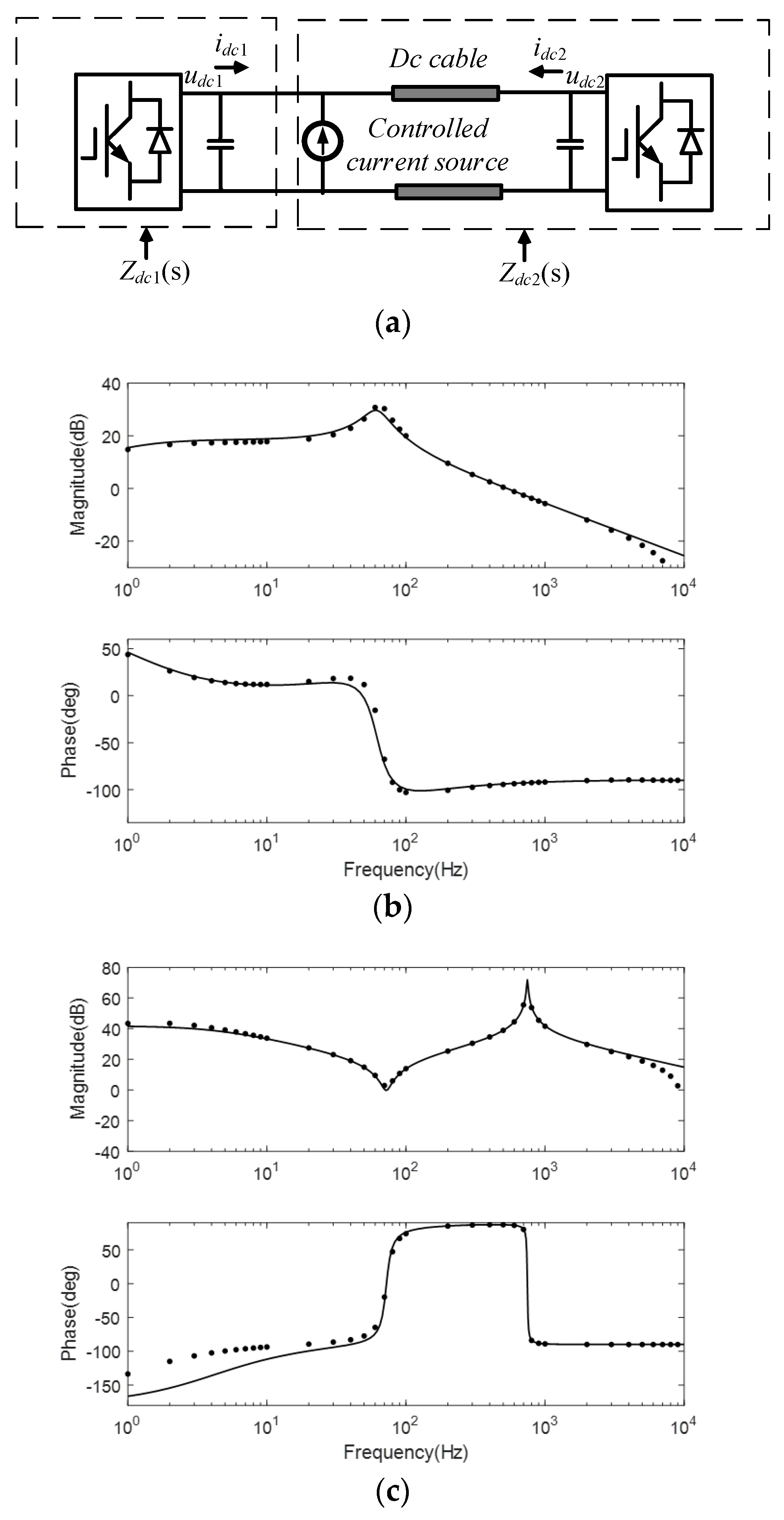
3.3. Verifying Impedance Modeling Through Perturbation Signal Testing

Perturbation signal testing is used to verify the accuracy of the proposed small-signal model. An AC current source should be placed parallel to the DC side of the system as an input signal, as Figure 6a shows. It is necessary to inject AC current at different frequencies to measure the DC side impedance at different frequencies. At each injection frequency, a simulation experiment is conducted. The DC voltage and DC current data of each experiment are analyzed by fast Fourier transformation. The components under the disturbance frequency are taken out, and the ratio of DC voltage and DC current is calculated as the calculated impedance [13]. Figure 6b,c shows the DC-side impedance verification of the DC system rectifier and inverter sides, respectively. The solid line in Figure 6b represents the analytical impedance of the rectifier converter as in (42), and the points represent the simulation results. Figure 6b represents the analytical impedance of the inverter station and the DC cable as (51), and the points represent the simulation results.

4. Stability Analysis of VSC–HVDC with Improved Virtual Impedance Control Strategy

According to the results of small signal modeling, the DC side of the voltage-controlled converter is modeled by a DC voltage source (Vs), in series with an output impedance (Zs), which equals to Zdc1. The DC side of the power-controlled converter and DC cable is modeled by a DC current source shunted with an input impedance (Zl), which equals to Zdc2. Figure 7 shows the equivalent impedance model of the system.
According to Kirchhoff’s law, the output voltage of the DC side Vdc (s) can be expressed by Formula (52). The stability of the DC system depends on the ratio of Zs to Zl, which is the open-loop transfer function of system Tm. DC voltage is predicted to be stable when Tm satisfies the Nyquist stability criterion [12,13,14]:
V d c ( s ) = ( v s ( s ) + i l ( s ) Z s ( s ) ) ( 1 1 + T m )
T m = Z s ( s ) Z l ( s ) .

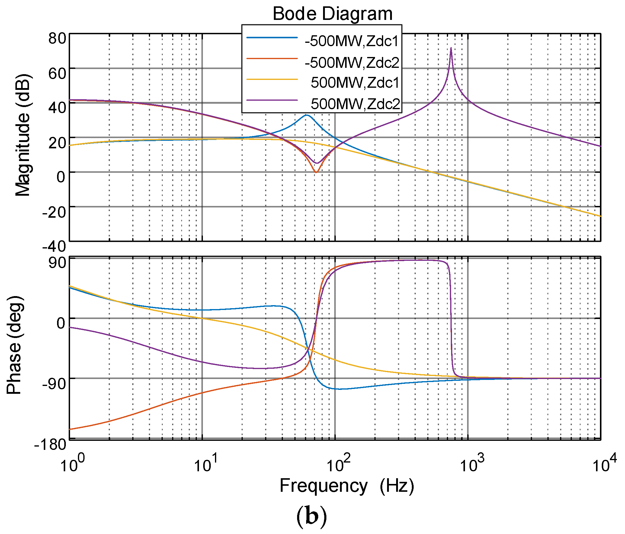
4.1. Impact of the Power Flow Direction

Figure 8a shows the Nichols plots of an open-loop transfer function Tm when the transmission power is ±500 MW and the length of the DC cable is 50 km. The traditional control strategy [13] shown in Figure 3 is adopted to a DC-voltage-controlled converter, and controller parameters are set as kpvdc = 15, kivdc = 100.
As shown in Figure 8a, the red line does not encircle (−180°, 0), and the VSC–HVDC system is predicted to be stable. The blue encircles (−180°, 0), and the VSC–HVDC system is predicted to be unstable.
Figure 8b shows the impedance frequency responses of Zdc1 and Zdc2 when the active power is set as ±500 MW. Compared with the yellow line and the blue line, in the mid-frequency band, the blue line shows negative damping while the yellow line does not. Zdc1 and Zdc2 intersect at the mid-frequency band due to the influence of DC cable impedance. The phase difference at the red line and blue line in the mid-frequency band is approximately 180°, so the DC voltage is predicted to oscillate. The stability analysis results are consistent with the simulation results in Figure 4.

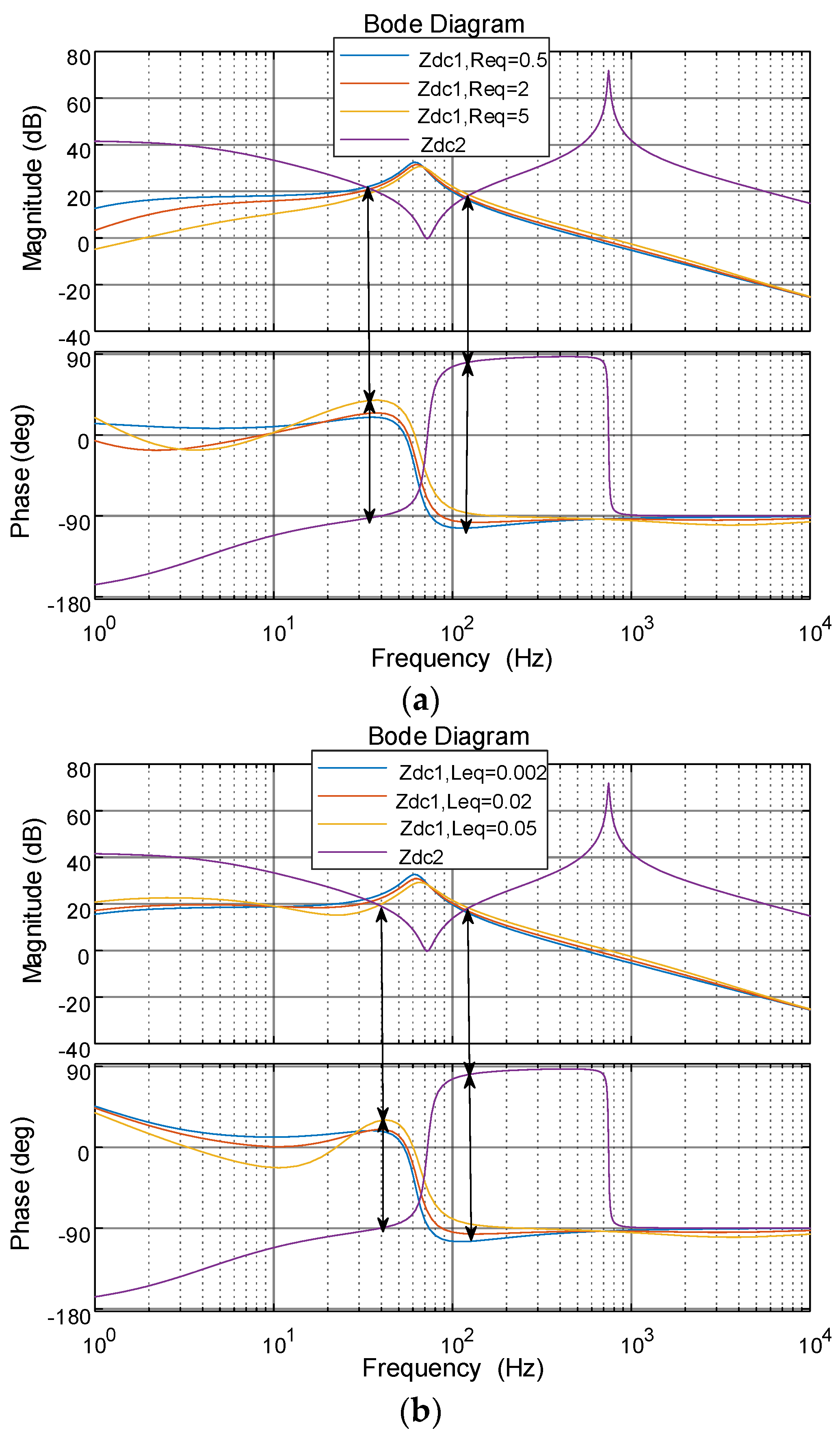
4.2. Impact of Virtual Impedance by Frequency Responses

Figure 9 shows the impedance frequency responses of Zdc1 and Zdc2 when the active power is set as −500 MW and the length of DC cable is 50 km. The proposed strategy in this paper is adopted for a DC-voltage-controlled converter, and the controller parameters are set as kpvdc = 15, kivdc = 100, and ki = 10. Figure 9a shows the impedance frequency responses of Zdc1 under a different Reqs. The pink line represents Zdc2 and the blue, red, and yellow lines represents Zdc1 when Req = 0.5, 2 and 5, respectively. The blue line shows that when the phase of Zdc1 impedance in the mid-frequency band is below −90°, the system exhibits negative damping. The phase difference at the intersection of the pink and blue lines in the mid-frequency band is approximately 180°, and the DC voltage is predicted to oscillate. The red and yellow lines show that when the phase of Zdc1 impedance in the mid-frequency band is above -90°, and the phase difference is less than 160 degrees, the DC voltage is predicted to stable. However, with the increase of Req, the phase difference at the intersection of the pink and blue lines in low-frequency bands increases, and the system tends to lose stability.
Figure 9b shows impedance frequency responses of Zdc1 under a different Leqs. The pink line represents Zdc2 and the blue, red, and yellow lines represent Zdc1 when Leq = 0.002, 0.02, and 0.05, respectively. Blue line shows that phase of Zdc1 impedance in mid-frequency band is below −90°, the system exhibits negative damping. The phase difference at the intersection of the pink and blue lines in the mid-frequency band is approximately 180°, and the DC voltage is predicted to oscillate. Red and yellow lines show that when the phase of Zdc1 impedance in the mid-frequency band is above −90°, and the phase difference is less than 160 degrees, the DC voltage is predicted to be stable. However, with the increase of Leq, the phase difference at the intersection of the pink and blue lines in the low-frequency band increases, and the system tends to lose stability.
The conclusion is that if the virtual impedance is too small, it will not be enough to suppress the oscillation. If the virtual impedance is too large, a new oscillation may occur in the low frequency band.

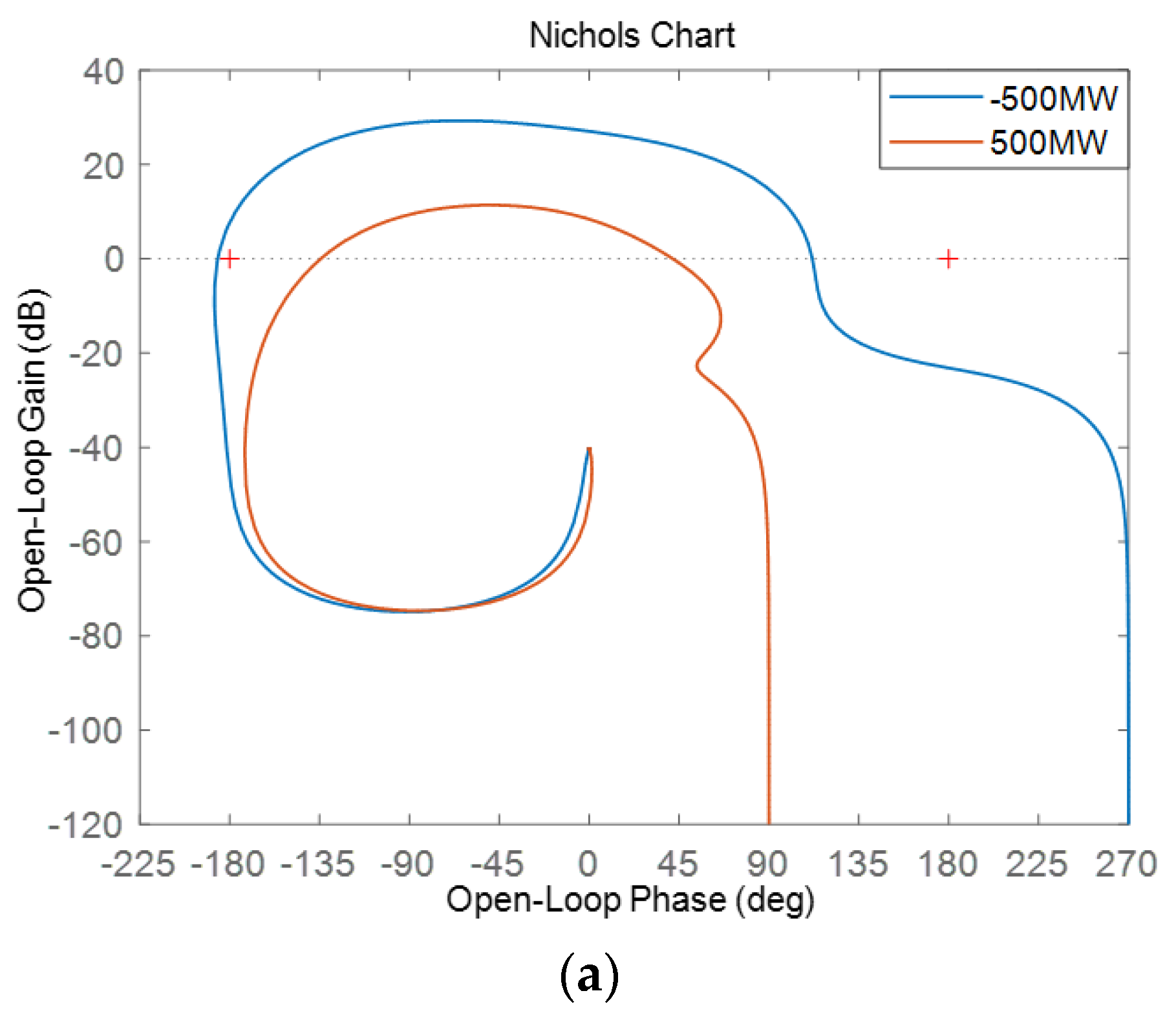
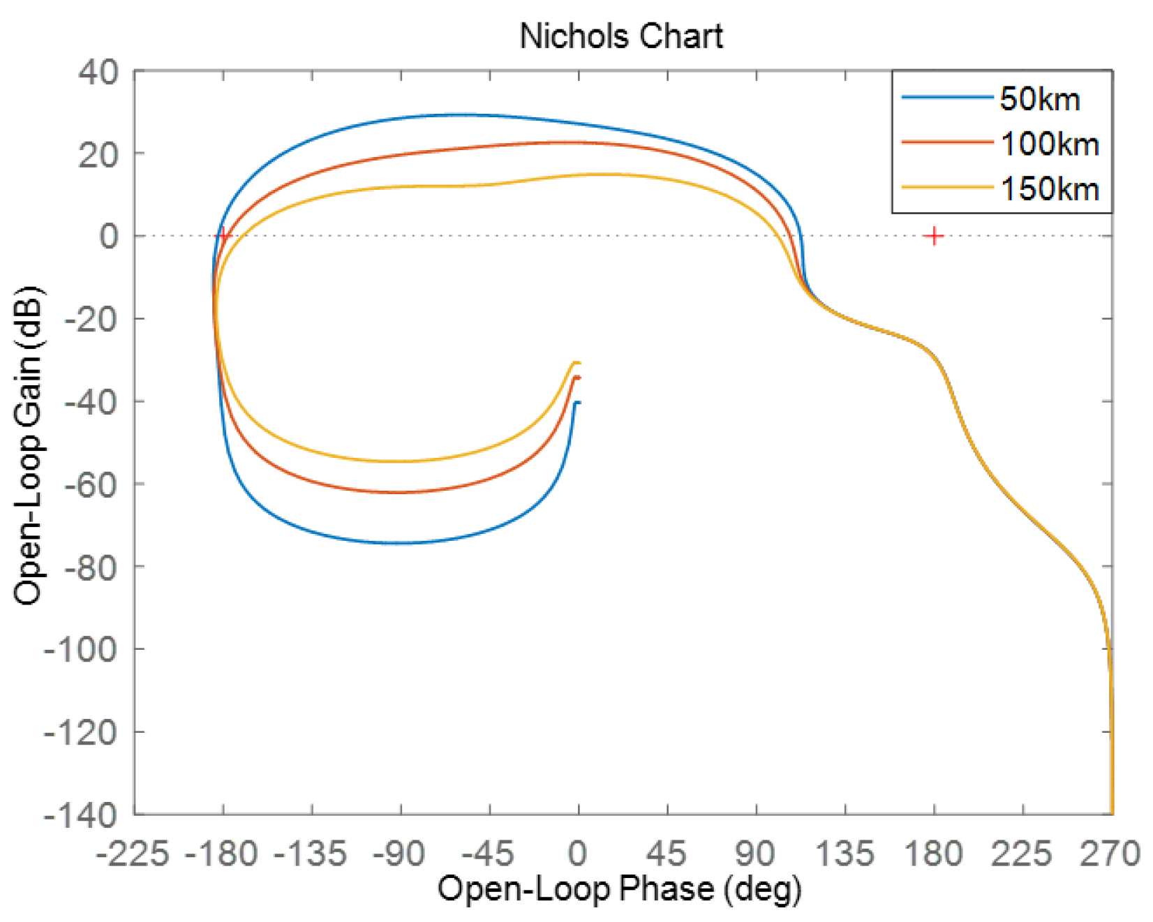
4.3. Impact of Virtual Impedance Parameters by Nichols Plots

Figure 10 shows the Nichols plots of Tm with different virtual impedance parameters. The DC cable length is 10 km and the transmission power is −500 MW. The proposed strategy in this paper is adopted to the DC-voltage-controlled converter, and the controller parameters are set as kpvdc = 15, kivdc = 100, and ki = 10. The blue, red, and yellow lines in Figure 10a show the Nichols plots of Tm when the virtual impedance parameters Req are 0.5 Ω, 2 Ω, and 5 Ω, respectively. Figure 10a shows that Tm encircles (−180°, 0), and the system is predicted to be unstable when Req = 0.5 Ω. The system is predicted to be stable when Req = 2 and 5 Ω. Increasing the Req value in a certain range helps improve the stability of the system. The phase margin of the system is insufficient to suppress DC-side oscillation when Req = 0.5 Ω.
The blue, red, and yellow lines in Figure 10b show the Nichols plots of Tm when virtual impedance parameters Leq are 0.002 Ω, 0.02 Ω, and 0.05 Ω, respectively. Figure 10b shows that Tm encircles (−180°, 0), and the system is predicted to be unstable when Leq = 0.002 Ω. The system is predicted to be stable when Leq = 0.02 and 0.05 Ω. Increasing the Leq value in a certain range helps improve the stability of the system. The phase margin of the system is insufficient to suppress DC-side oscillation when Leq = 0.002 Ω.

4.4. Impact of DC Cable Length

Figure 11 shows the Nichols plots of the open-loop transfer function Tm under different lengths of DC cable when the transmission power is −500 MW. The control parameters are kpvdc = 15, kivdc = 100, ki = 10, Req = 0.5 Ω, and Leq = 0.002 Ω. The blue, red and yellow lines in Figure 11 represent the Nichols plots of Tm at DC cable lengths of 50, 100, and 150 km, respectively. As shown in Figure 11, the Nichols plot gradually approaches (−180°, 0), with a decrease in DC cable length. The Nichols plot encircles (−180°, 0), and the system is predicted to be unstable when the DC cable length is reduced to 50 km.

4.5. Impact of DC Side Capacity

Figure 12 shows the Nichols plots of the open-loop transfer function Tm under a different capacitance of the DC side capacity when the transmission power is −500 MW. The control parameters are kpvdc = 15, kivdc = 100, ki = 10, Req = 0.5 Ω, and Leq = 0.002 Ω. The blue, red, and yellow lines in Figure 12 represent the Nichols plots of Tm at the DC side capacity of 300, 450, and 600 µf, respectively. As shown in Figure 12, the Nichols plot gradually approaches (−180°, 0), with a decrease in the DC side capacity. The Nichols plot encircles (−180°, 0), and the system is predicted to be unstable when the DC side capacity is reduced to 300 µf.
From the above stability analysis, it can be concluded that there are three main factors affecting the stability of the system—power flow [24], main circuit parameters, and controller parameters. Among the main circuit parameters, the most important factors are the length of the circuit and the capacitance of the DC side. According to the stability, analysis results in 4.4 and 4.5. The stability margin of the system can be improved by increasing the DC capacitance and DC cable length. When the main circuit parameters are determined and the power flow is determined, the stability of the system can also be improved by optimizing the controller settings.

4.6. Impact of Grid Impedance

Figure 13 shows the Nichols plots of the open-loop transfer function Tm under different grid impedance when the transmission power is −500 MW. The control parameters are kpvdc = 15, kivdc = 100, ki = 10, and Leq = 0.02 Ω. The blue and red lines in Figure 13 represent the Nichols plots of Tm when Ln = 1 and 5 mH, respectively. The blue line does not encircle (−180°, 0), while the red line encircles (−180°, 0), which means and DC-side oscillations are more likely to occur in weaker power grids. The yellow line in Figure 13 represents the Nichols plot of Tm when Ln = 5 mH and Req = 2. The yellow line does not encircle (−180°, 0), which means the system is predicted to be stable after choosing appropriate virtual impedance parameters.

5. Simulation Verification

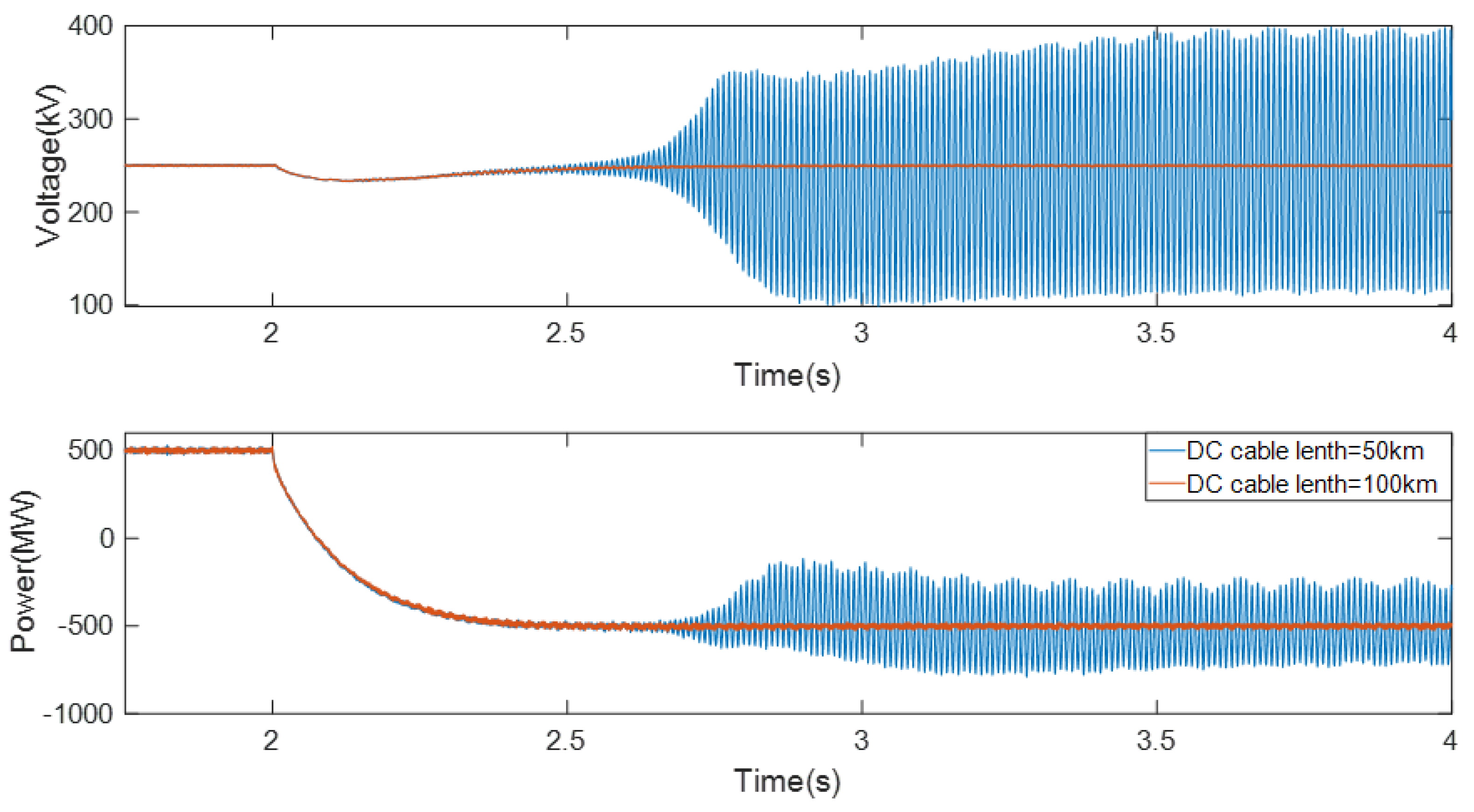
5.1. Impact of DC Cable Length

Figure 14 shows the simulation results of the VSC–HVDC system with virtual impedance control strategy under different DC cable lengths. The voltage control parameters are kpvdc = 15, kivdc = 100, ki = 10, Req = 0.5 Ω, and Leq = 0.002 Ω. At 2 s, the steady-state power command value is set from 500 MW to −500 MW. As shown in Figure 14, the blue line indicates the simulation results when the DC cable length is 50 km, and the red line indicates 100 km. The DC voltage in the blue line drops by approximately 5% and begins to oscillate, and the system loses stability. The DC voltage in the red line drops by approximately 5%, smoothly restoring the instruction value, and the system remains stable. The simulation results are consistent with the theoretical analysis in Section 4.4.

5.2. Impact of DC Side Capacity

Figure 15 shows the simulation results of the VSC–HVDC system with a virtual impedance control strategy under a different DC side capacity. The voltage control parameters are kpvdc = 15, kivdc = 100, ki = 10, Req = 0.5 Ω, and Leq = 0.002 Ω. At 2 s, the steady-state power command value is set from 500 MW to −500 MW. As shown in Figure 15, the blue line indicates the simulation results when the DC side capacity is 300 µf, and the red line indicates 450 µf. The DC voltage in the blue line drops by approximately 5% and begins to oscillate, and the system loses stability. The DC voltage in the red line drops by approximately 5%, smoothly restoring the instruction value, and the system remains stable. The simulation results are consistent with the theoretical analysis in Section 4.5.

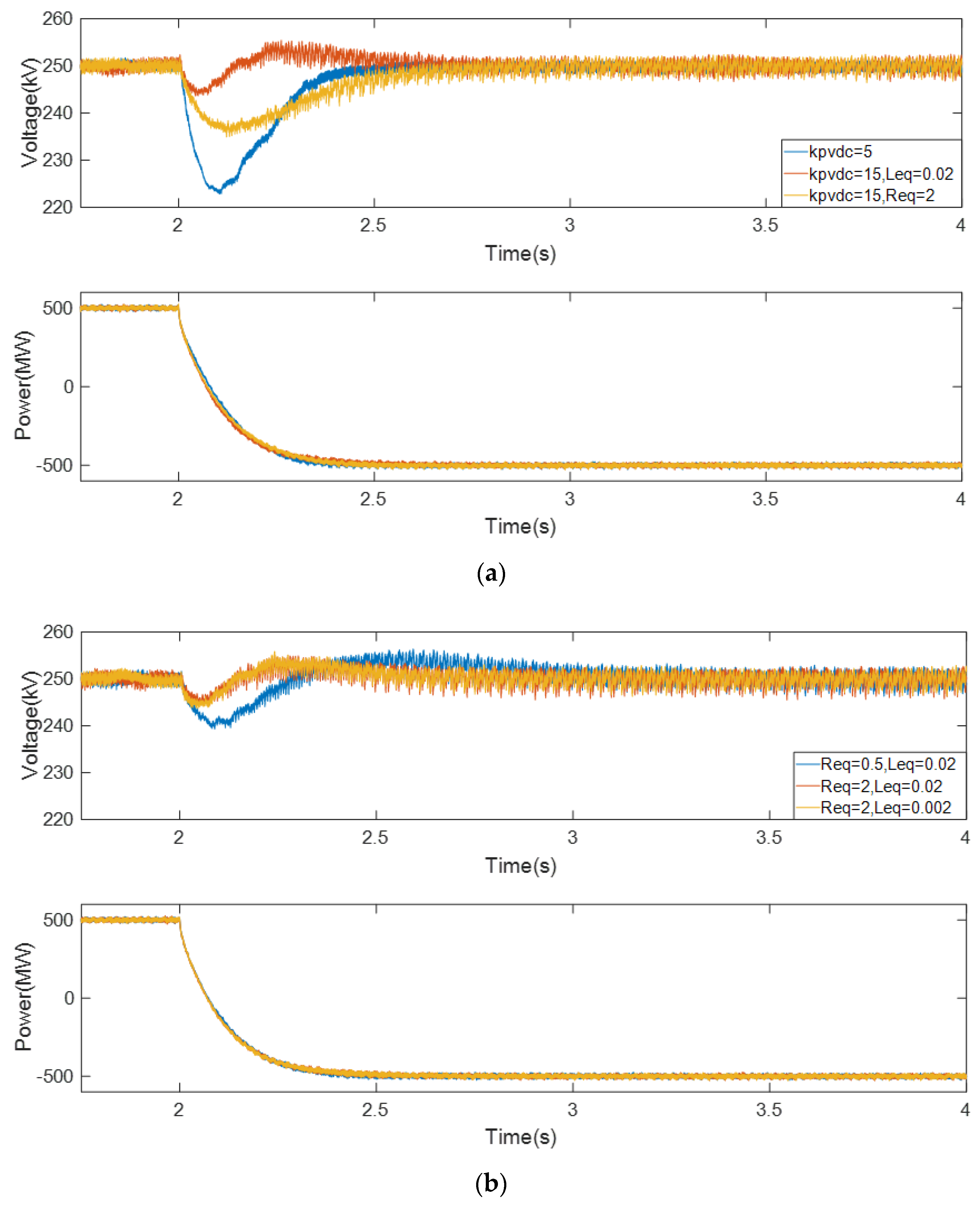
5.3. Dynamic Performance Comparison

According to [13], reducing the value of kpvdc can improve the output impedance of the DC-voltage-controlled converter, thereby reinforcing the stability of the system. However, this condition influences the dynamic performance of the control. This paper compares the dynamic performance of the two control strategies. Similarly, the DC cable length is 50 km, and the active power instruction changes from 500 MW to −500 MW at 2 s. As shown in Figure 16a, the blue line represents the DC voltage under the traditional control strategy [13]. When kpvdc = 5 and kivdc = 100, the red line represents the DC voltage under the proposed control strategy when kpvdc = 15, kivdc = 100, ki = 10 and Req = 2 Ω, and the yellow line represents the DC voltage under the proposed control strategy when kpvdc = 15, kivdc = 10, ki = 10, and Leq = 0.02 Ω. The DC voltage in the blue line drops by approximately 9% when the instruction value is changed and gradually increases to the instruction value. The DC voltage in the red line drops by only 2% when the instruction value is changed and increases the instruction value by more than 2%. The DC voltage in the yellow line drops by only 4% when the instruction value is changed and gradually increases to the instruction value. The dynamic performance of the proposed control strategy is better than that of the traditional control method.
Figure 16b compares system DC voltages under the proposed control strategy with different virtual impedance parameters when kpvdc = 15, kivdc = 100 and ki = 10. The blue line represents Req = 0.5, Leq = 0.02 Ω, the red line represents Req = 2 Ω, Leq = 0.02 Ω, and the yellow line represents Req = 2 Ω, Leq = 0.002 Ω. From the comparison of these three lines, it can be seen that the speed of DC voltage regulation mainly depends on Req. As can be seen from Figure 9a, increasing Req can reduce the amplitude response of Zdc1 in the low-frequency band. However, increasing Leq has little effect on the amplitude response of Zdc1 in the low-frequency band, as in Figure 9b.

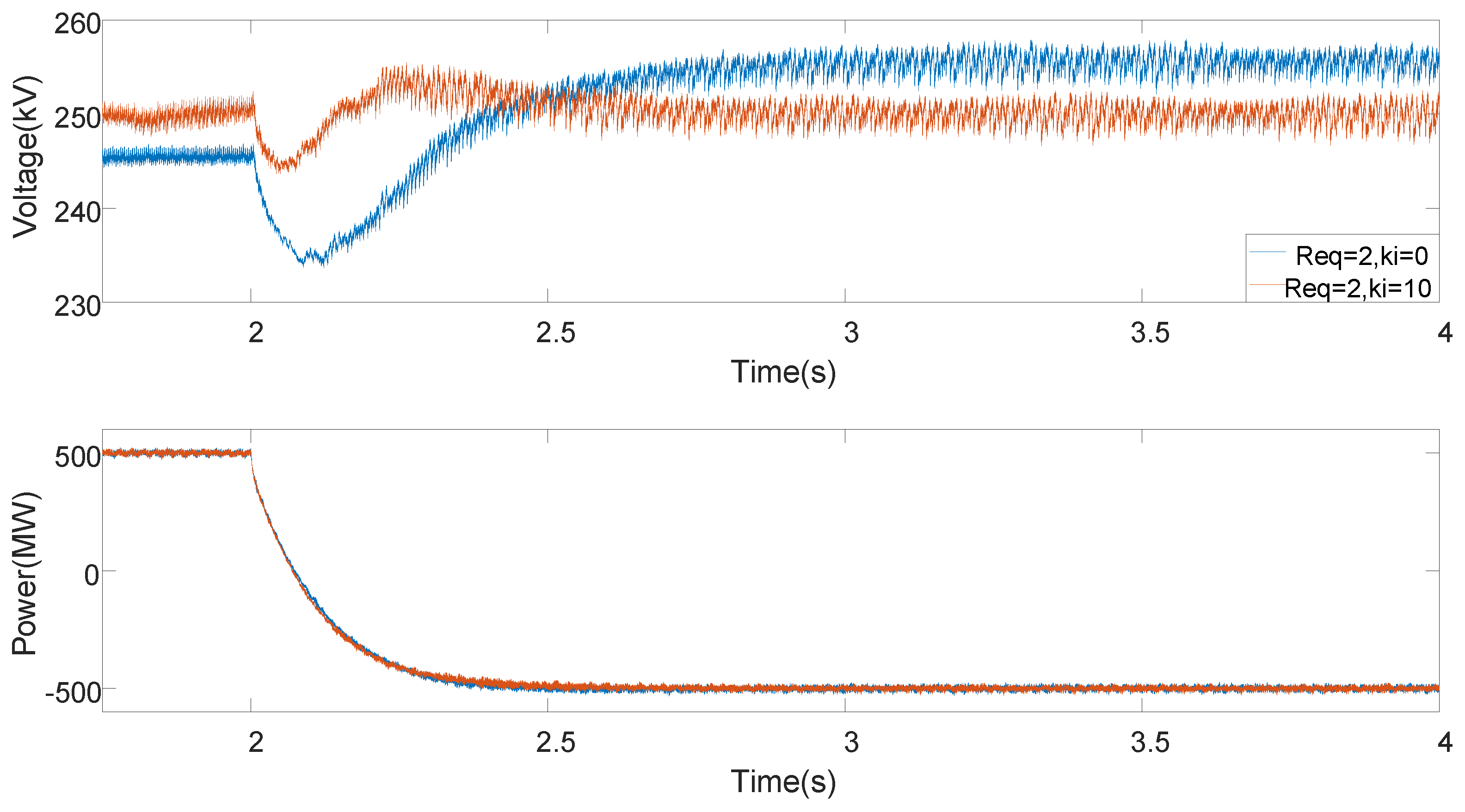
5.4. Steady State Error Elimination

On the basis of the previous analysis, although the traditional virtual impedance control strategy can enhance the transmission capacity of the system, it causes the steady-state error of DC voltage. Figure 17 shows the comparison of two virtual impedance control strategies. The length of the DC cable is 50 km. At 2 s, the steady-state power command value is set from 500 MW to −500 MW.
The DC voltage in the blue line represents the traditional virtual impedance, shown as the yellow frame in Figure 5, and the controller parameters are kpvdc = 15, kivdc = 100, and Req = 2 Ω. The DC voltage in the red line represents the proposed control strategy, with kpvdc = 15, kivdc = 100, Req = 2 Ω, and ki = 10. Under the two control strategies, the DC voltage fluctuates in a short time and a small range only, and the active power can steadily step down. The DC voltage shown by the red line is close to the instruction value of 250 kV, and the steady-state error of the blue line is approximately 5 kV in both power flow directions, which are consistent with the theoretical analysis. The simulation results show that the improved virtual impedance control method can improve the stability of the DC system and eliminate the steady-state error of the DC voltage caused by the virtual impedance.

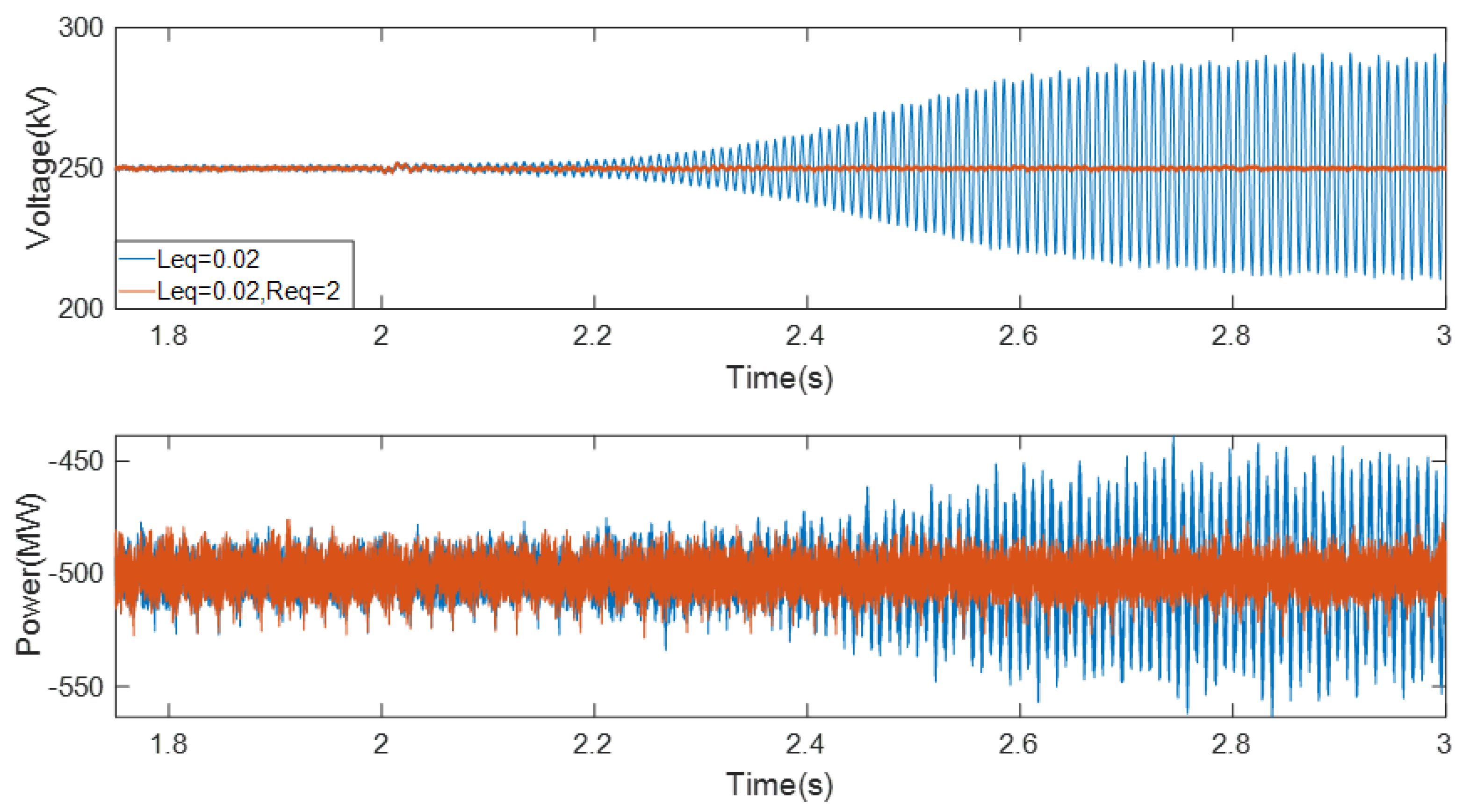
5.5. Impact of Gird Impedance

Figure 18 shows the simulation results of the VSC–HVDC system with a virtual impedance control strategy under a different grid impedance. The voltage control parameters are kpvdc = 15, kivdc = 100, ki = 10, and the transmission power is set as −500 MW. At 2 s, the grid impedance is switched from 1 mH to 5 mH. The blue line in Figure 18 indicates the simulation results when the virtual impedance parameter is Leq = 0.02 Ω. The DC voltage in the blue line begins to oscillate, and the system loses stability. The red line in Figure 18 indicates the simulation results when virtual impedance parameters are Leq = 0.02 Ω and Req = 2 Ω. The DC voltage in the red line stays stable, and the system remains stable. The simulation results are consistent with the theoretical analysis in Section 4.6.

6. Conclusions

This paper investigates the stability of VSC–HVDC operation in a bidirectional power flow mode. DC cable length affects the reverse power transmission power of the system. An improved virtual impedance control strategy is presented to increase the reverse power transmission power of the system. A system stability analysis based on the impedance model is applied to the proposed control strategy. System stability is affected by the power flow, controller parameters, DC cable length, and DC side capacity.
(1)
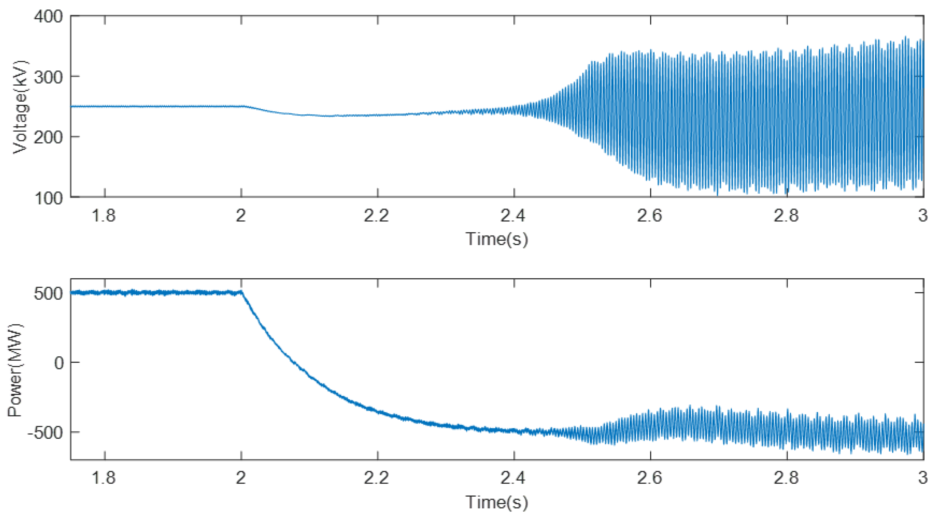
DC-side oscillation occurs when the transmission power of the system is large. The maximum transmission power of a DC voltage-controlled converter to a power-controlled converter is less than that in the opposite transmission direction.
(2)
The shorter the DC cable is, the more easily the oscillation of DC voltage will occur.
(3)
The smaller the DC side capacity is, the more easily the oscillation of DC voltage will occur.
(4)
The weaker the AC grid strength is, the more easily the DC side oscillation will occur.
(5)
Appropriate virtual impedance parameters can improve system stability. The phase margin of the system is insufficient to suppress DC-side oscillation when the virtual impedance parameter is small. If the virtual impedance parameters, Req or Leq, are too large, then the system will enter a new unstable state.
The simulation results show that the proposed improved control strategy can eliminate the steady-state error of DC voltage caused by virtual impedance and maintain the advantage of a virtual impedance strategy to improve system stability. The proposed control method has better dynamic performance compared to the traditional control method.

Author Contributions

All the authors have contributed to this paper in different aspects. Y.L. proposed the original concept and wrote the original draft. K.L. acted as supervisor and gave suggestions on paper improvement. S.Z., X.L., and Q.H. helped with software simulation and methodology improvement.

Funding

This research was funded by [Nation Key Research and Development Program of China] grant number [2017YFB0903700] And The APC was funded by [2017YFB0903700].

Conflicts of Interest

The authors declare no conflict of interest.

References

  1. Flourentzou, N.; Agelidis, V.G.; Demetriades, G.D. VSC-Based HVDC Power Transmission Systems: An Overview. IEEE Trans. Power Electron. 2009, 24, 592–602. [Google Scholar] [CrossRef]
  2. Yang, J.; Liu, K.; Yu, Y.; Qin, L.; Le, J. Small Signal Modeling for VSC-HVDC Used in AC Grid Interconnection. Proc. CSEE 2015, 35, 2177–2184. [Google Scholar]
  3. Zhang, L.; Nee, H.P. Multivariable feedback design of VSC-HVDC connected to weak ac systems. In Proceedings of the IEEE Bucharest PowerTech, Bucharest, Romania, 28 June–2 July 2009; pp. 1–8. [Google Scholar]
  4. Kumars, R.; Arash, M.; Jose, I.C.; Alvaro, L.; Pedro, R. A Generalized Voltage Droop Strategy for Control of Multiterminal DC Grids. IEEE Trans. Ind. Appl. 2015, 51, 607–618. [Google Scholar]
  5. Zhang, L.; Nee, H.P.; Harnefors, L. Analysis of Stability Limitations of a VSC-HVDC Link Using Power-Synchronization Control. IEEE Trans. Power Syst. 2011, 26, 1326–1337. [Google Scholar] [CrossRef]
  6. Zhang, L.; Harnefors, L.; Nee, H.P. Interconnection of Two Very Weak AC Systems by VSC-HVDC Links Using Power-Synchronization Control. IEEE Trans. Power Syst. 2011, 26, 344–355. [Google Scholar] [CrossRef]
  7. Wen, B.; Dong, D.; Boroyevich, D.; Mattavelli, P.; Shen, Z. Impedance-Based Analysis of Grid-Synchronization Stability for Three-Phase Paralleled Converters. IEEE Trans. Power Electron. 2015, 31, 675–687. [Google Scholar] [CrossRef]
  8. Yuan, H.; Yuan, X.; Hu, J. Modeling of Grid-Connected VSCs for Power System Small-Signal Stability Analysis in DC-Link Voltage Control Time-scale. IEEE Trans. Power Syst. 2017, 32, 3981–3991. [Google Scholar] [CrossRef]
  9. Kalcon, G.O.; Adam, G.P.; Anaya-Lara, O.; Lo, S.; Uhlen, K. Small-Signal Stability Analysis of Multi-Terminal VSC-Based DC Transmission Systems. IEEE Trans. Power Syst. 2012, 27, 1818–1830. [Google Scholar] [CrossRef]
  10. Beerten, J.; D’Arco, S.; Suul, J.A. Identification and Small-Signal Analysis of Interaction Modes in VSC MTDC Systems. IEEE Trans. Power Deliv. 2016, 31, 888–897. [Google Scholar] [CrossRef]
  11. Li, Y.; Tang, G.; He, Z.; An, T.; Yang, J.; Wu, Y.; Kong, M. Damping Control Strategy research for MMC based HVDC system. Proc. CSEE 2016, 36, 5492–5503. [Google Scholar]
  12. Xu, L.; Fan, L.; Miao, Z. DC Impedance-Model-Based Resonance Analysis of a VSC–HVDC System. IEEE Trans. Power Deliv. 2014, 30, 1221–1230. [Google Scholar] [CrossRef]
  13. Amin, M.; Molinas, M.; Lyu, J.; Cai, X. Impact of Power Flow Direction on the Stability of VSC-HVDC Seen from the Impedances Nyquist Plot. IEEE Trans. Power Electron. 2016, 32, 8204–8217. [Google Scholar] [CrossRef]
  14. Middlebrook, R.D. Input Filter considerations In Design and Application of Switching Regulators. In Proceedings of the IEEE Power Electronics Specialists Conference, Cleveland, OH, USA, 8 June 1976; pp. 366–382. [Google Scholar]
  15. Sun, J. Impedance-Based Stability Criterion for Grid-Connected Inverters. IEEE Trans. Power Electron. 2011, 26, 3075–3078. [Google Scholar] [CrossRef]
  16. Pinares, G.; Bongiorno, M. Modeling and Analysis of VSC-Based HVDC Systems for DC Network Stability Studies. IEEE Trans. Power Deliv. 2015, 31, 848–856. [Google Scholar] [CrossRef]
  17. Pinares, G.; Bongiorno, M. Analysis and Mitigation of Instabilities Originated From DC-Side Resonances in VSC-HVDC Systems. IEEE Trans. Ind. Appl. 2016, 52, 2807–2815. [Google Scholar] [CrossRef]
  18. Song, Y.; Breitholtz, C. Nyquist Stability Analysis of an AC-Grid Connected VSC-HVDC System Using a Distributed Parameter DC Cable Model. IEEE Trans. Power Deliv. 2016, 31, 898–907. [Google Scholar] [CrossRef]
  19. Amin, M.; Molinas, M. Small-Signal Stability Assessment of Power Electronics Based Power Systems: A Discussion of Impedance- and Eigenvalue-Based Methods. IEEE Trans. Ind. Appl. 2017, 53, 5014–5030. [Google Scholar] [CrossRef]
  20. Yu, X.; Salato, M. An Optimal Minimum-Component DC–DC Converter Input Filter Design and Its Stability Analysis. IEEE Trans. Power Electron. 2014, 29, 829–840. [Google Scholar]
  21. Cespedes, M.; Xing, L.; Sun, J. Constant-Power Load System Stabilization by Passive Damping. IEEE Trans. Power Electron. 2011, 26, 1832–1836. [Google Scholar] [CrossRef]
  22. Radwan, A.A.A.; Mohamed, A.R.I. Linear Active Stabilization of Converter-Dominated DC Microgrids. IEEE Trans. Smart Grid. 2012, 3, 203–216. [Google Scholar] [CrossRef]
  23. Wu, M.; Lu, D.C. A Novel Stabilization Method of LC Input Filter With Constant Power Loads Without Load Performance Compromise in DC Microgrids. IEEE Trans. Ind. Electron. 2015, 62, 4552–4562. [Google Scholar] [CrossRef]
  24. Wu, W.; Chen, Y.; Luo, A.; Zhou, L.; Zhou, X.; Yang, L.; Huang, X. A Virtual Phase-Lead Impedance Stability Control Strategy for the Maritime VSC-HVDC System. IEEE Trans. Ind. Inf. 2018, 14, 5475–5486. [Google Scholar] [CrossRef]
  25. Tang, X.; Zhang, K.; Xu, Q.; Chen, S.; Tan, W. Control strategy for enlarging the transmission capacity of VSC-HVDC systems supplying passive networks. Trans. China Electron. 2016, 31, 44–51. [Google Scholar]
  26. Paquette, A.D.; Divan, D.M. Virtual Impedance Current Limiting for Inverters in Microgrids With Synchronous Generators. IEEE Trans. Ind. Appl. 2015, 51, 1630–1638. [Google Scholar] [CrossRef]
  27. Lu, X.; Wang, J.; Guerrero, J.M.; Zhao, D. Virtual-Impedance-Based Fault Current Limiters for Inverter Dominated AC Microgrids. IEEE Trans. Smart Grid 2018, 9, 1599–1612. [Google Scholar] [CrossRef]
  28. Rizqiawan, A.; Fujita, G.; Funabashi, T.; Nomura, M. Impact of a virtual impedance on the input admittance of a grid—Connected inverter. IEEE Trans. Electr. Electron. 2013, 8, 190–198. [Google Scholar] [CrossRef]
  29. Li, Y.; Tang, G.; Ge, J.; He, Z.; Pang, H.; Yang, J.; Wu, Y. Modeling and Damping Control of Modular Multilevel Converter Based DC Grid. IEEE Trans. Power Syst. 2018, 33, 723–735. [Google Scholar] [CrossRef]
Figure 1. VSC–HVDC used in AC grid interconnection.
Applsci 09 03184 g001
Figure 2. System and phase-locked loop (PLL) references.
Applsci 09 03184 g002
Figure 3. Control structure of the converters.
Applsci 09 03184 g003
Figure 4. DC-link voltage and the active power of the VSC–HVDC system.
Applsci 09 03184 g004
Figure 5. Proposed control structure of the converters.
Applsci 09 03184 g005
Figure 6. Frequency response of the impedance and verification. The solid line represents the model prediction, and the black points denote the simulation. (a) Disturbance signal testing. (b) Impedance of the DC voltage-controlled converter (c). Impedance of the power-controlled converter.
Applsci 09 03184 g006
Figure 7. Equivalent model of the VSC–HVDC system.
Applsci 09 03184 g007
Figure 8. (a) Nichols plots of Tm when transmission power is ±500 MW. (b) Impedance frequency responses of Zdc1 and Zdc2 when transmission power is ±500 MW.
Applsci 09 03184 g008aApplsci 09 03184 g008b
Figure 9. Impedance frequency responses of Zdc1 and Zdc2 under different equivalent virtual impedance values (a) Req and (b) Leq.
Applsci 09 03184 g009
Figure 10. Nichols plots of Tm under different equivalent virtual impedance values (a) Req; (b) Leq.
Applsci 09 03184 g010
Figure 11. Nichols plots of Tm under different DC cable lengths.
Applsci 09 03184 g011
Figure 12. Nichols plots of Tm under different DC side capacities.
Applsci 09 03184 g012
Figure 13. Nichols plots of Tm under a different grid impedance.
Applsci 09 03184 g013
Figure 14. DC-link voltage and active power of the VSC–HVDC system under different DC cable lengths.
Applsci 09 03184 g014
Figure 15. DC-link voltage and active power of the VSC–HVDC system under different DC side capacity.
Applsci 09 03184 g015
Figure 16. DC-link voltage and active power of the VSC–HVDC system (a) under the proposed control strategy and traditional control strategy [13] and (b) under the proposed control strategy with different virtual impedance parameters.
Applsci 09 03184 g016
Figure 17. DC-link voltage and active power of the VSC–HVDC system under the proposed control strategy and traditional virtual impedance.
Applsci 09 03184 g017
Figure 18. DC-link voltage and active power of the VSC–HVDC system under different gird impedance.
Applsci 09 03184 g018
Table 1. Simulation parameters.
ParametersValues
Converter and AC systemSystem capacity Sn/MW500
Line voltage of grid ug/kV110
DC voltage Vdc/kV250
Grid internal resistance Rn0.2
Grid frequency ω0/Hz50
Grid internal inductance Ln/H1 × 10−3
Filter reactor inductance Lc/H4.5 × 10−2
Filter reactor resistance Rc0.2
DC side capacitance Cdc/μf300
DC cableDC cable resistance Rd/Ω/km1.39 × 10−2
DC cable inductance Ld/H/km1.59 × 10−4
DC cable capacitance Cd/F/km2.31 × 10−7
ControllerDC voltage outer loop kpvdc/kivdc15/100
Current inner loop kpc/kic0.5/0.1
Active power outer loop kpp/kip1/10
Phase locked loop kpPLL/kiPLL10/100

