
First-Principles Study of Linear and Nonlinear Optical Properties of Multi-Layered Borophene


1
Department of Physics, Michigan Technological University, Houghton, MI 49931, USA
2
DEVCOM Army Research Laboratory, Weapons, and Materials Research Directorate, ATTN: FCDD-RLW, Aberdeen Proving Ground, Aberdeen, MD 21005-5069, USA
*
Authors to whom correspondence should be addressed.
Computation 2021, 9(9), 101; https://0-doi-org.brum.beds.ac.uk/10.3390/computation9090101
Submission received: 25 August 2021
/
Revised: 11 September 2021
/
Accepted: 14 September 2021
/
Published: 18 September 2021
(This article belongs to the Section Computational Chemistry)
Abstract
:Anisotropic materials are of great interest due to their unique direction-dependent optical properties. Borophene, the two-dimensional analog of graphene consisting of boron atoms, has attracted immense research interest due to its exciting anisotropic electronic and mechanical properties. Its synthesis in several structural polymorphic configurations has recently been reported. The present work reports the layer-dependent optical absorption and hyperpolarizabilities of the buckled borophene (δ6-borophene). The results, based on density functional theory, show that multilayer borophene is nearly transparent with only a weak absorbance in the visible region, reflecting its anisotropic structural characteristics. The static first-order hyperpolarizability significantly increases with the number of layers, due mainly to interactions among the frontier orbitals in multilayer borophene. Transparency in the visible region combined with enhanced nonlinear optical properties makes the multilayer borophene important for future photonics technologies.
1. Introduction
In recent years, there have been intense interest in two-dimensional (2D) materials due to their remarkable properties, leading to a wide range of potential applications at the nanoscale. These 2D materials have various electronic properties, including metallic, semiconducting, superconducting, and even topological insulator properties. They are considered the new generation of nanomaterials with many applications, including field-effect transistors (FETs), photovoltaic solar cells, optical devices, spintronics, and valley electronics [1,2,3,4,5,6,7,8,9]. In line with advances in the fabrication of new 2D materials, exciting developments concerning atomically thin boron sheets, referred to as borene or borophene, have occurred [10,11]. In its 2D lattice, several structural configurations were predicted, which were composed of fused boron clusters forming either a stripped anisotropic structure (i.e., δ6-borophene) [10] or an atomically flat honeycomb structure with hollow hexagons [12]. Furthermore, scanning tunneling microscopy measurements showed that borophene has a planar configuration with anisotropic corrugation [10]. Such anisotropic materials are of considerable interest because of their unique combination of polarization- or direction-dependent electrical, optical, and thermoelectric properties.
It has also been noted that boron sheets grown on Ag (111) surface are metallic β12 and χ3 sheets, with β12 being gapless with Dirac cones [11,13]. Both β12 and χ3 sheets are atomically flat in a triangular lattice with atomic vacancies. Following the theoretical predictions of the stability of the borophene [14,15,16,17,18,19,20], its synthesis on metallic substrates including Ag, Au, and Cu [21,22] has now extended the possibility of the realization of the boron nanostructure-based devices [23,24,25,26]. It is worth mentioning that, while borophene has been synthesized on metallic substrates, it has not yet been isolated. Thus, most of the understanding of its properties arises from simulation studies based on density functional theory.
The successful fabrications of borophene have inspired many follow-up works, especially for the δ6-borophene. This δ6-borophene, due to its anisotropic structure, possesses the highest young’s modulus of all other polymorphs. Its value along one of the directions is higher than that of graphene, and it depicts a negative Poisson’s ratio that results from the out-of-plane buckling [10,27]. In addition, the tubular configuration based on δ6-borophene has a higher 2D Young’s modulus than any other known carbon and noncarbon nanostructures [28]. The dynamic and thermodynamic instability in its free-standing form arises from its high stiffness originating from the directional bonding [29]. Owing to its anisotropic structure, however, the δ6-borophene shows highly anisotropic metallic properties [10,11,30], which are very different from the semi-metallic graphene [31] and semiconducting transition metal dichalcogenides (TMDCs) [32]. Furthermore, the monolayer of δ6-borophene is predicted to have high optical transparency and electrical conductivity along the un-corrugated direction, which may rival graphene [33]. Relative to its group-IV counterpart graphene, borophene exhibits anisotropic dependence of its electronic and magnetic properties due to its structural configuration, which can be exploited for orientation-dependent applications [30].
Despite considerable progress in the synthesis and structure-property relationship understanding of borophene through extensive experimental and theoretical studies, its nonlinear optical properties (NLO) remain unexplored. There have been two recent theoretical studies of the NLO properties of finite B-clusters, specifically bowl-type B36 nanosheets. The effects of different alkali earth metals (e.g., Li), and transition metal adsorption on B36 nanosheet, on the static hyperpolarizability, was investigated [34,35]. Because borophene was predicted to be transparent [36], knowing its NLO properties has become more critical since there is a general lack of transparent NLO materials for applications ranging from coherent photon sources to sensor and eye protection.
The unique properties of 2D materials relative to that of the bulk, in general, motivate the exploration of their layered configurations for future device fabrication [1]. Recently synthesized graphene, silicene, boron-nitride nanosheets, transition-metal dichalcogenides (TMDs), and black phosphorus possess novel properties that differ from or exceed their bulk counterparts [1,3,4,5,37,38]. Research into layered materials with novel properties is a vigorous area of research due to its scientific importance and possible practical applications. For example, for some of the layered metal dichalcogenides (e.g., MoS2), the transition from an indirect semiconductor in bulk to a direct semiconductor in a monolayer [39] inspired investigation into their optoelectronic properties. Many other 2D materials are under study. Among these is an exceptional class of materials, multi-layered borophene. The optical properties of monolayer borophene have been studied. However, the scientific literature is still lacking in terms of the investigation of multi-layered borophene.
Moreover, the layer dependence of the optical properties of borophene is comparable to that of graphene and antimonene, investigated in our previous work [40]. In the present work, we report a comprehensive study of layer-dependent linear and NLO properties of δ6-borophene (also called striped borophene). Calculations were performed within the framework of sum-over-state (SOS) (for absorbance) and coupled perturbation method for (hyper)polarizabilities using the density functional theory (DFT) approach, with a focus on optoelectronic device applications such as photodetectors, light-emitting diodes, and photovoltaic devices which, in general, require low absorption while preserving a high electrical conductivity [41,42]. Throughout the text, δ6-borophene is labeled as borophene.
2. Computational Method
DFT-based calculations were performed with projector augmented wave (PAW) [43] potentials using the Vienna ab initio simulation package (VASP, V5.4.4) [44]. The generalized gradient approximation (GGA) proposed by Perdew–Burke–Ernzerhof (PBE) was used to treat the electron exchange and correlation [45]. Contributions from the van der Waals interactions were incorporated by using Grimme’s semi-empirical dispersive D2 term [46]. A plane-wave basis set with a kinetic energy cutoff of 500 eV was used.
Multilayer borophene was simulated in a periodic unit cell, which consisted of 2, 4, 6, and 8 atoms of boron for monolayer, bilayer, trilayer, and quad-layer, respectively. A vacuum of 15 Å perpendicular to the surface was used. The structural configurations were fully relaxed with residual forces smaller than 0.001 eV/Å on each atom. The energy convergence value between two consecutive steps was chosen to be 10−8 eV. The Monkhorst–Pack scheme with a (25 × 40 × 1) grid for the k-point sampling was used, as also reported previously [36].
Additional calculations were performed using the 2 × 2 and 3 × 3 periodic supercells to assess the reliability and accuracy of the two-atom periodic unit cell. The calculated bond lengths, band structure, and density of states nearly remained the same, suggesting a periodic unit cell containing two atoms for monolayer borophene sufficient for further calculations.
In 2D materials, e.g., graphene, low-energy optical absorption can be calculated using the imaginary part of the dielectric function ( via the ‘sum-over-states’ (SOS) method [47]. The fraction of photon energy (E = ħω) absorbed by a multilayer system can be expressed in terms of absorbance, as
where w is the angular frequency of the incident light, Lz is the thickness of the absorber, taken here as the length of a periodic supercell simulating the multilayer system along the direction perpendicular to the surface, and c is the speed of light. The thickness Lz is defined as the sum of the vacuum and interlayer distances for a multilayer system. In this way, the calculated absorbance is independent of the size of the vacuum in the z-direction of the periodic supercell [40,48] and is equivalent to the absorbance calculated using the expression [48], with being the imaginary part of the polarizability per unit area. Note that, in the periodic supercell method applied to 2D materials, the vacuum in the z-direction is arbitrary, leading to an inverse dependence of the dielectric function [40]. The k-point sampling was increased to (96 × 160 × 1) to describe the optical spectra accurately. Furthermore, can be expressed as:
Here, c and v refer to conduction and valence band states, respectively, k is the wave vector, uv(c),k represents the wave function with a periodicity of the lattice, and Ω is the volume of the supercell [47].
To calculate the nonlinear optical (NLO) properties, we employed a cluster model representing multilayer borophene in terms of the nanoflakes, fragments of the configurations obtained from the periodic supercell calculations. These multi-layered nanoflakes are expected to have properties similar to those of sheets.
The static linear polarizability (α) and first hyperpolarizability (β) were calculated with a coupled perturbed method using DFT. is given by while the anisotropy in α is calculated as:
and,
To be consistent with the results presented for the linear optical properties, we used the PBE functional form and D2 dispersion correction as implemented in the Gaussian16 program package [49]. The convergence criteria for the RMS density matrix and total energy were set at 10−8 and 10−6 eV, respectively. Note that including both the polarization and diffuse functions in the basis set is essential to describe the NLO properties [50] accurately. However, this becomes computationally expensive when the number of atoms increases from the monolayer to the quad-layer of borophene. Therefore, to calculate the layer-dependence of hyperpolarizabilities for multilayer borophene, we used a 6–31 G basis, which is reliable in terms of predicting the static components of both α and β, as recently demonstrated for graphene, phosphorene, the h-BN monolayer, and their nanoflake heterostructures [50].
3. Results and Discussions
3.1. Structural and Electronic Properties
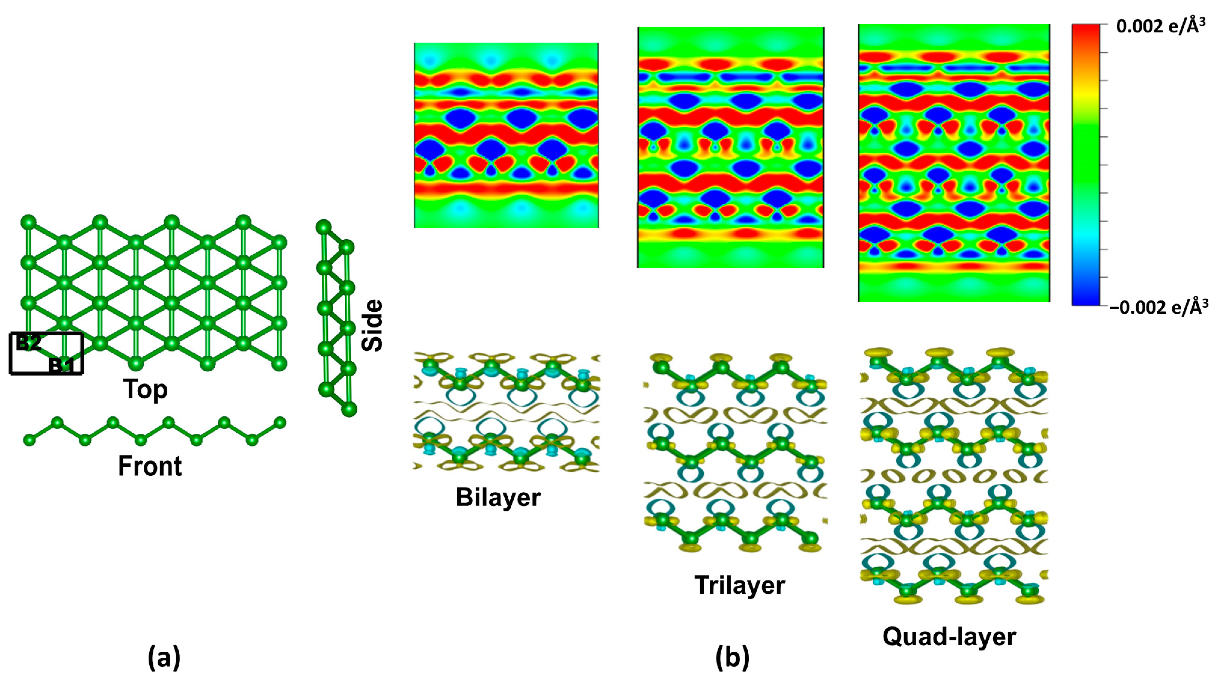
Figure 1a shows the ball and stick representation of the multilayer borophene. Unlike the planar hexagonal configuration of graphene, δ6-borophene adopts a buckled triangular structure. Its space group is Pmmn with two B atoms per unit cell [10]. As shown, the parallel linear chains of B–B bonds exist along its armchair direction while buckling occurs along its zigzag path. In the equilibrium configuration of a monolayer, the calculated lattice constants, a = 2.87 Å, and b = 1.61 Å, agree with previously reported theoretical and experimental [10,51] values. The bond length along the b direction (i.e., B1–B1 or B2–B2) is 1.61 Å, and B1–B2 is 1.87 Å.
We follow the previously obtained DFT results [52] for the bilayer configuration, which reported the AA stacking sequence as the energetically preferred configuration. Subsequently, we consider the stacking sequence of AAA and AAAA for trilayer and quad-layer borophene. Table 1 lists the interlayer binding energy and interlayer distances obtained after performing constraint-free optimization of multilayer borophene.
The charge density difference plots for the bilayer, trilayer, and quad-layer show a noticeable change between the layers, indicating the presence of the interlayer interaction (Figure 1b). The calculated interlayer separation is 2.58, 2.63, and 2.60 Å for bilayer, trilayer, and quad-layer borophene. This separation is comparatively smaller than that of the other 2D materials, e.g., ~3.1 Å for bilayer phosphorene [2] as well as bilayer MoS2 [53]. Therefore, the results find that the interlayer interaction in layered borophene is slightly higher than the other 2D layers.
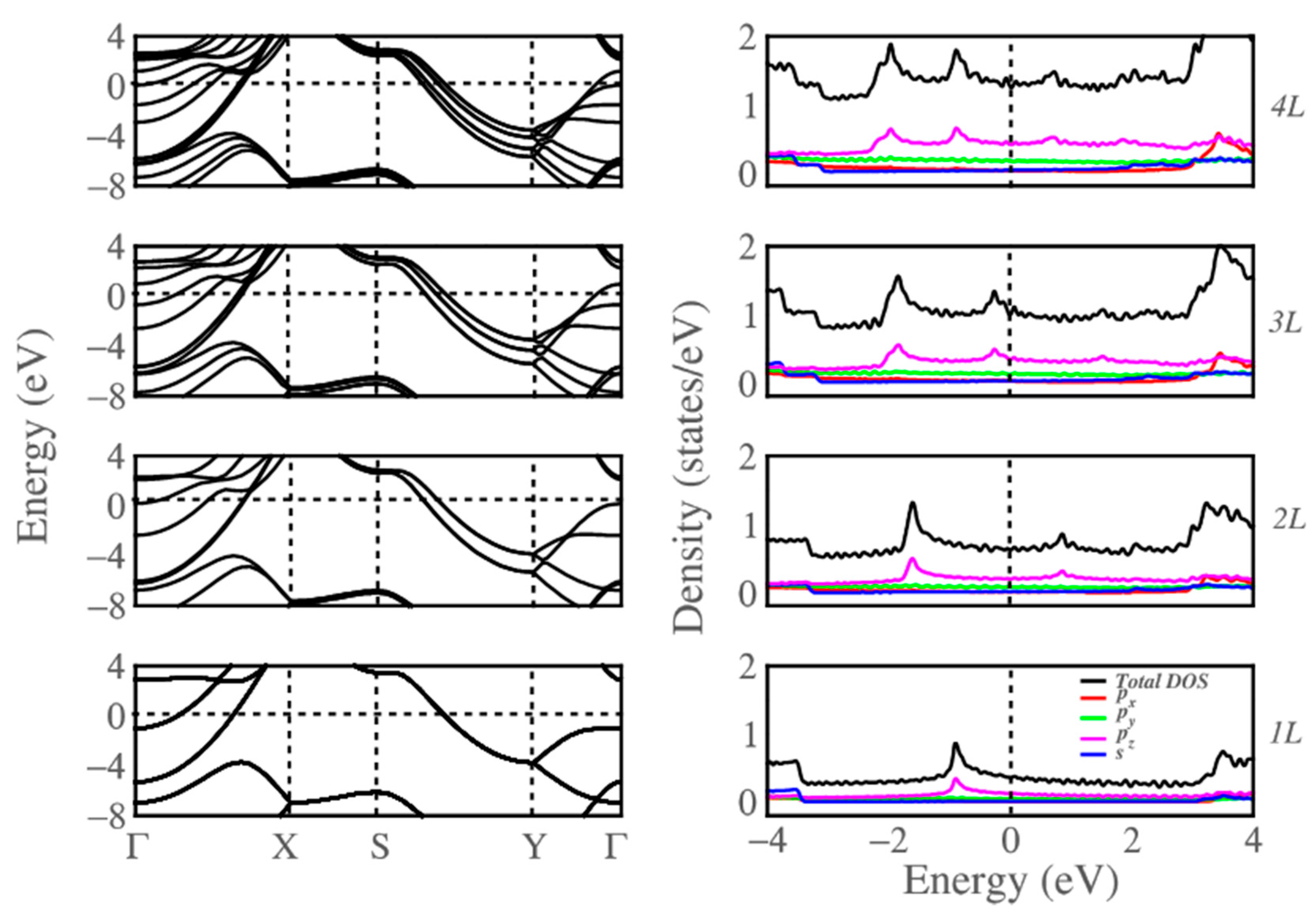
Figure 2 shows the band structure of multilayer borophene computed within the DFT approximation. For the monolayer, two bands cross the Fermi energy at distinct locations in the Brillouin zone, suggesting this to be metallic, in agreement with previous calculations [54], with a noticeably wide energy gap of 4.3 eV in the band structure in the Γ (Γ-Y direction). More bands cross the Fermi level for the multilayer cases because of the band splitting due to interlayer interactions retaining the metallic nature with increasing thickness. We note that the local energy gaps resulting from the buckling at Γ and S still exist. The energy gap at the Γ point (Γ-Y direction) decreases from 4.32 eV (monolayer) to 2.12 eV (quad layer) as a result of the increasing of the band splitting with the increasing of the thickness. Since no splitting exists at the S point, the energy gap at this high symmetry point barely changes from the monolayer to the quad-layer. One, therefore, expects the multilayer borophene to exhibit highly anisotropic electronic properties, including confinement of electrical conductivity along the un-corrugated direction. The band splitting around Γ along the Y-Γ direction near Fermi can estimate the strength of the interlayer interaction in multilayer borophene relative to other 2D layered materials, such as MoS2 and black phosphorous. Our calculated band splitting for borophene is ~4 eV, higher than ~1 eV in bilayers of MoS2 and black phosphorus [55], suggesting that the interlayer interaction in the former is more substantial than those in the other 2D materials.
The partial density of states (PDOS), representing the relative contribution of each orbital to the total DOS, also reflects the changes that occurred in going from monolayer to quad-layer Figure 2. For example, a shift in the peak positions in the valence band is accompanied by an increase in the number of bands in the band structure of multilayer borophene.
3.2. Optical Absorbance
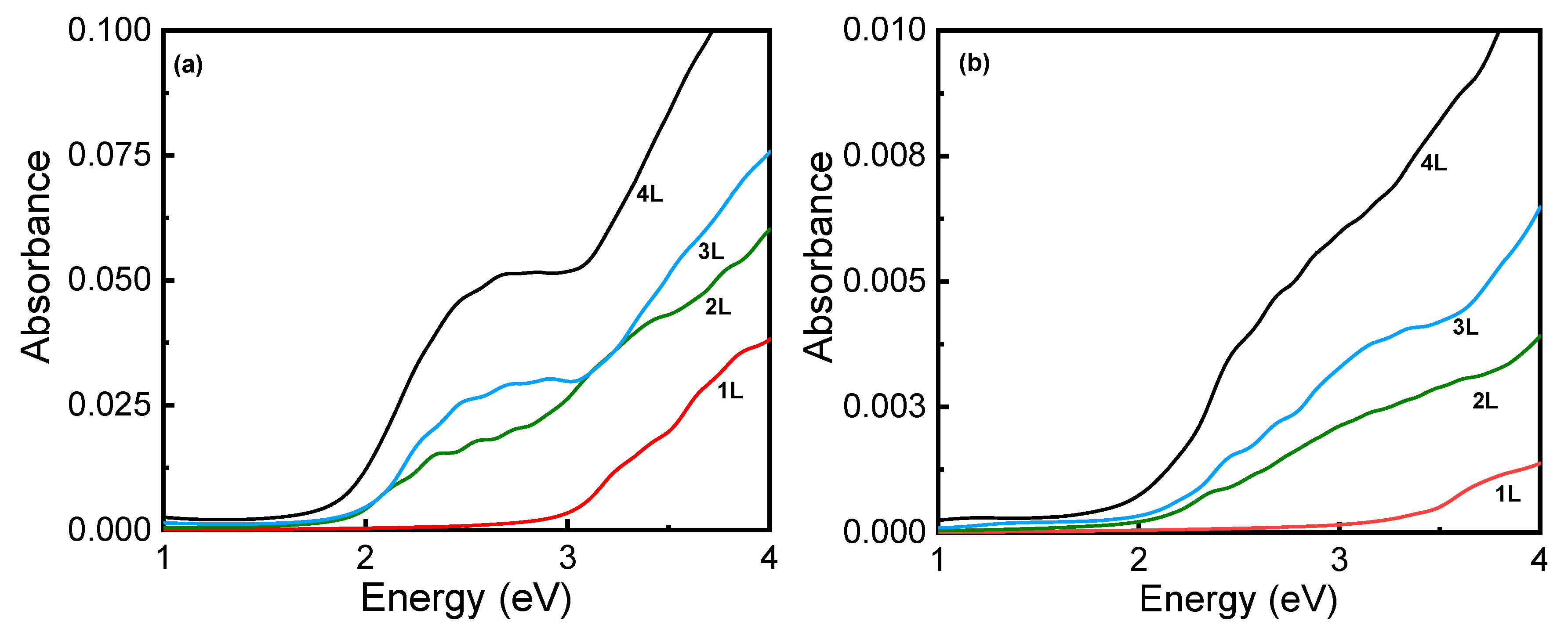
Considering the enhanced stability and the modifications in the electronic properties of borophene with an increasing number of layers, it is worthwhile to examine their effects on the optical properties, specifically the optical absorbance, as shown in Figure 3. It is clear from the figure that the in-plane absorbance (for X and Y polarized light) shows broad transparency in the visible region between ~1.8–3.1 eV with less than 0.2% absorbance. For monolayer borophene, the results agree with the previously published results [36] and the results obtained using the imaginary part of polarizability per unit area [40,48].
With an increase in the number of layers, a broad shoulder appears at about ~2.6 eV in the X direction, specifically for the tri- and quad-layer structures, which is likely associated with an intra-band transition between the partially occupied bands along the Γ−X direction (Figure 2). Furthermore, the anisotropic structure is reflected in the calculated absorbance with the X-component, which though still remarkably low, shows a significant layer-dependence in the UV region.
3.3. Nonlinear Optical Properties: Hyperpolarizabilities
In 2D materials, the crystal structure plays an essential role in nonlinear optical (NLO) properties. For centrosymmetric materials such as graphene, the odd-order hyperpolarizabilities, including the first-hyperpolarizability, vanish. For borophene, however, a zigzag type buckled structure removes the inversion symmetry and, therefore, NLO effects of all orders can have non-zero values.
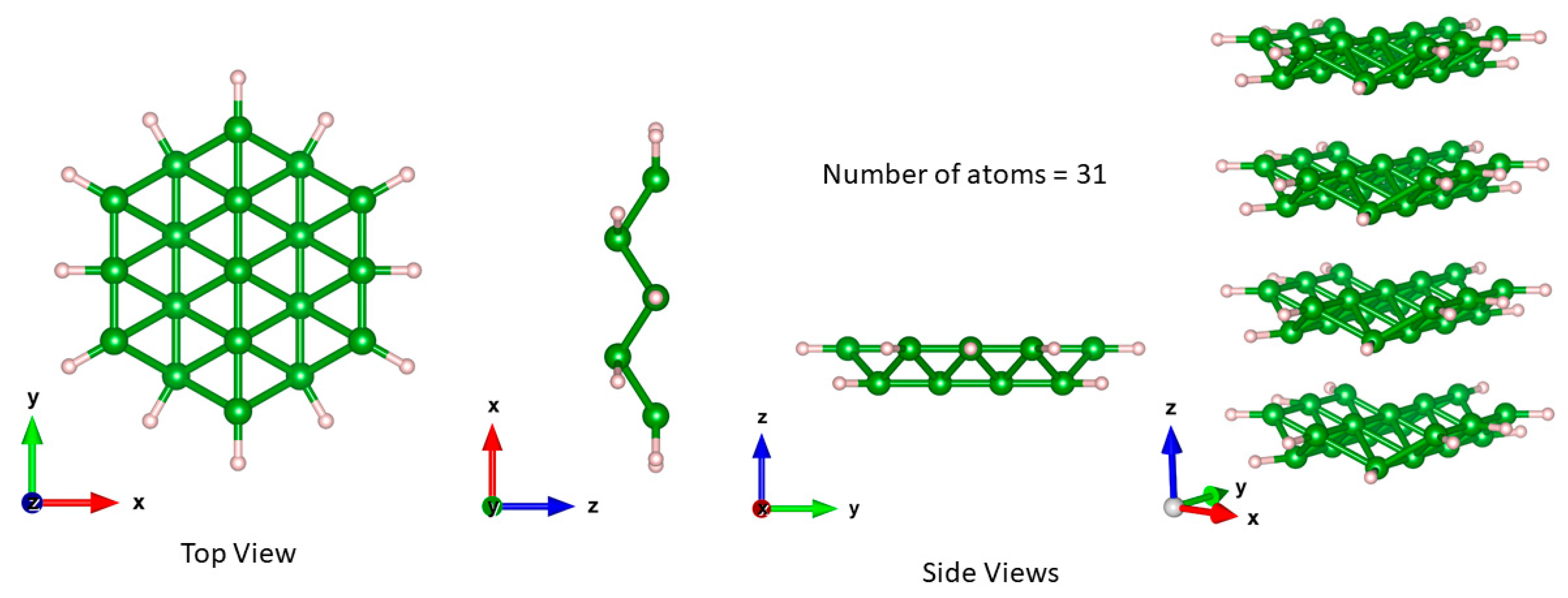
In a cluster approximation, simulation of borophene requires passivation of the edge atoms to retain its structural coordination, which is similar to that of a sheet. In the present work, we use B19H12 clusters for monolayer nanoflakes, as displayed in Figure 4.
Table 2 represents the non-zero components of the static polarizability and first dipole hyperpolarizability β. The calculated results show that the mean dipole polarizability value defined as increases with the number of layers. This layer-dependent increase can also be seen in the non-zero components (xx, yy, and zz). Furthermore, this increase in polarizability with the number of layers is more prominent along the zz direction than the xx and yy direction, indicating the influence of interlayer interaction on polarizability.
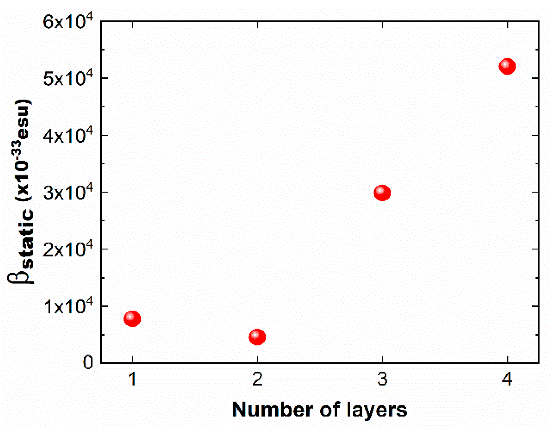
A similar trend is also exhibited by the calculated dipole moment. Considering that β is related to the dipole moment, one would expect a similar increase in β from mono- to quad-layer configurations [56]. Indeed, as displayed in Figure 5, The results show a significant increase in the static |β| from mono- to quad-layer borophene, but this does not occur monotonically. Similar to the polarizability, the hyperpolarizability is also influenced by the interlayer interaction, as can be seen from the sharp increase in the zzz component values from the monolayer to the quad-layer [15]. It should be pointed out that, for the monolayer, the calculated static |βTotal| value of 7766 × 10−33 esu is significantly higher than that reported for the bowl-type B36 structure [34,35]. The difference in the predicted values can be attributed to the structural differences between buckled borophene nanoflake, as used here, versus the bowl-type B36 structure used in previous calculations [19]. Note that the hyperpolarizability calculations use the “esu” unit while the experimental measurement has the unit of pm/V. The conversion factor is 1 pm/V = 2.387 × 10⁻⁹ esu.
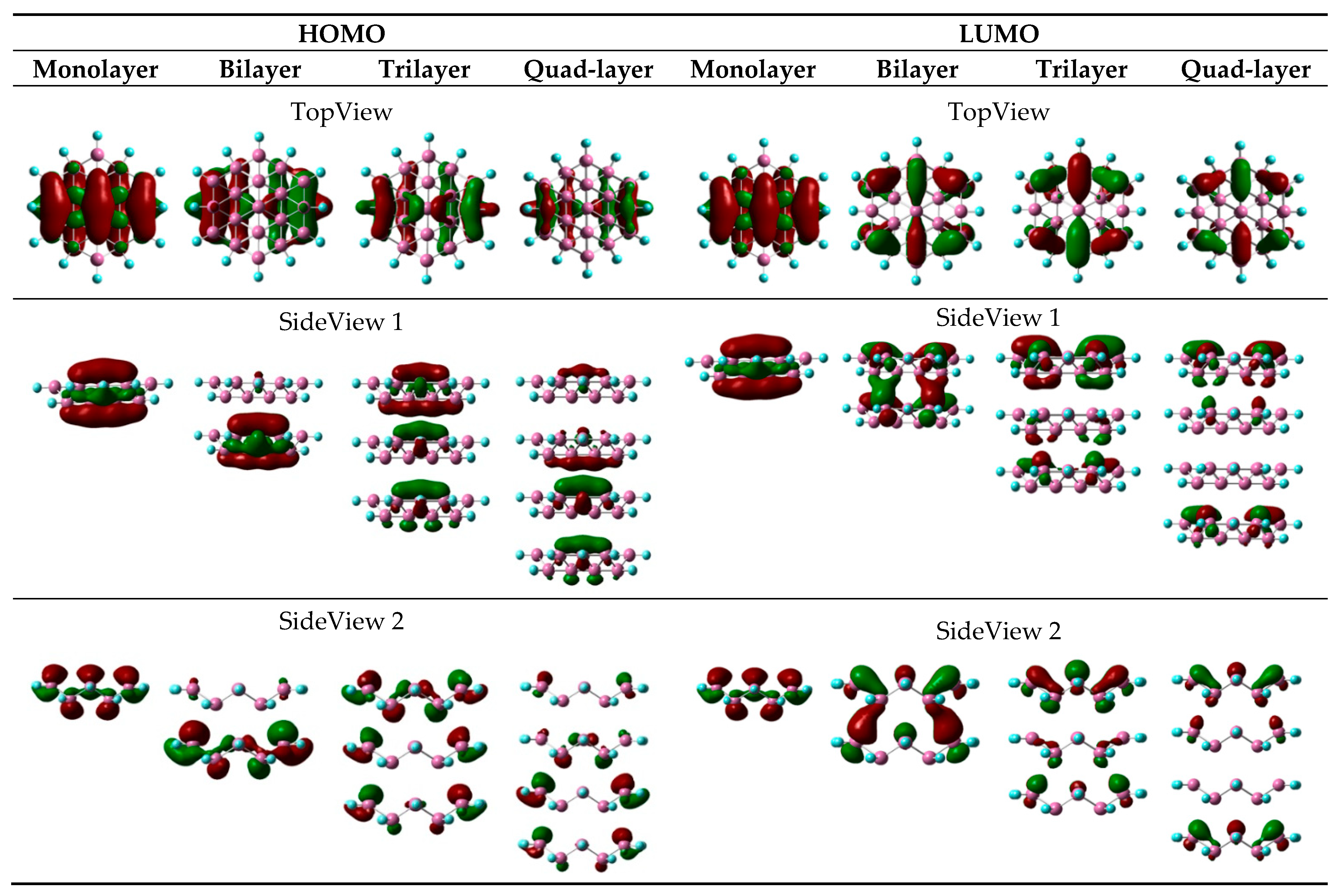
It is worthwhile to examine the interaction among the frontier molecular orbitals (highest occupied molecular orbital (HOMO) and lowest unoccupied molecular orbital (LUMO)) in the multilayer nanoflakes and their contribution to the (hyper) polarizabilities. It is expected that the interlayer interaction in multilayer borophene is likely to result in changes in the nature of the frontier molecular orbitals with an increase in the number of layers.
Figure 6 displays HOMOs and LUMOs of multilayer borophene, showing changes in their composition from mono- to quad-layer. These orbitals appear to arise from the intra-layer interactions in the monolayer, while the inter-layer interactions of B atoms dominate the case of the quad-layer. For example, one can see the dominant contributions in the formation of HOMOs and LUMOs from the 2p orbitals of B atoms, which are not located on the same layer. Though not significant enough to firmly bind the layers, this interlayer interaction suggests the importance of interface-driven optical responses in multilayer borophene.
4. Summary
We have presented linear and nonlinear optical properties of multilayer borophene following the atomic configuration classified as δ6-borophene, which has a highly anisotropic structure. The electrical and optical properties of borophene are found to be significantly dependent on the number of layers. The calculated DFT results show that multilayer borophene maintains anisotropic metallic features while offering transparency in the visible region. Moreover, a large splitting of ~1.7 eV at Γ points to significant interlayer interactions in multilayer borophene relative to the other multilayer 2D materials. The optical absorption is also anisotropic for multilayer borophene with higher absorption in the X-direction relative to the Y direction, enabling the fabrication of performance-controlled optoelectronic devices. Furthermore, due to the non-centrosymmetric structure, borophene exhibits a non-zero first dipole hyperpolarizability value (β), which increases with the number of layers that have significantly enhanced values; this can be attributed to the modifications in the nature of the frontier molecular orbitals due to the interlayer interactions in multilayer borophene. Multi-layered borophene shows promise for the integration of anisotropic electronics, optics, and optoelectronics in high-performance devices.
Author Contributions
Conceptualization, R.P. and S.P.K.; methodology, G.S. and S.K.; software, G.S. and S.K.; validation, G.S., S.K., R.P. and S.P.K.; formal analysis, G.S., S.K. and R.P.; investigation, G.S. and S.K.; resources, R.P. and S.P.K.; data curation, S.K. and G.S.; writing—original draft preparation, S.K. and G.S.; writing—review and editing, R.P. and S.P.K.; visualization, G.S. and S.K.; supervision, R.P. and S.P.K.; project administration, R.P. and S.P.K.; funding acquisition, R.P. and S.P.K. All authors have read and agreed to the published version of the manuscript.
Funding
The research was partially supported by the Army Research Office (ARO) through Grant No. W911NF-14-2-0088.
Data Availability Statement
Data is contained within the article and can also be obtained from the corresponding authors.
Acknowledgments
The authors thank Ashok Kumar, Maximilian Seel, and Dhanshree Pandey for the helpful discussions. SK acknowledges the financial support provided by the Elizabeth and Richard Henes Center for Quantum Phenomena, Michigan Technological University. Computational resources at Michigan Technological University, including the SUPERIOR high-performance computing cluster, were utilized.
Conflicts of Interest
The authors declare no conflict of interest.
References
- Ponraj, J.S.; Xu, Z.-Q.; Dhanabalan, S.C.; Mu, H.; Wang, Y.; Yuan, J.; Li, P.; Thakur, S.; Ashrafi, M.; Mccoubrey, K. Photonics and optoelectronics of two-dimensional materials beyond graphene. Nanotechnology 2016, 27, 462001. [Google Scholar] [CrossRef]
- Zhang, T.; Lin, J.H.; Yu, Y.M.; Chen, X.R.; Liu, W.M. Stacked bilayer phosphorene: Strain-induced quantum spin Hall state and optical measurement. Sci. Rep. 2015, 5, 1–13. [Google Scholar] [CrossRef] [Green Version]
- Wang, J. Two-dimensional semiconductors for ultrafast photonic applications. In Proceedings of the Optical Components and Materials XII, San Francisco, CA, USA, 9–11 February 2015; p. 935902. [Google Scholar]
- Luo, A.-P.; Liu, M.; Wang, X.-D.; Ning, Q.-Y.; Xu, W.-C.; Luo, Z.-C. Few-layer MoS 2-deposited microfiber as highly nonlinear photonic device for pulse shaping in a fiber laser. Photonics Res. 2015, 3, A69–A78. [Google Scholar] [CrossRef]
- Sobon, G. Mode-locking of fiber lasers using novel two-dimensional nanomaterials: Graphene and topological insulators. Photonics Res. 2015, 3, A56–A63. [Google Scholar] [CrossRef]
- Xia, F.; Wang, H.; Xiao, D.; Dubey, M.; Ramasubramaniam, A. Two-dimensional material nanophotonics. Nat. Photonics 2014, 8, 899–907. [Google Scholar] [CrossRef]
- Vela, A.; Moutinho, M.; Culchac, F.; Venezuela, P.; Capaz, R.B. Electronic structure and optical properties of twisted multilayer graphene. Phys. Rev. B 2018, 98, 155135. [Google Scholar] [CrossRef]
- Hong, S.-Y.; Dadap, J.I.; Petrone, N.; Yeh, P.-C.; Hone, J.; Osgood, R.M., Jr. Optical third-harmonic generation in graphene. Phys. Rev. X 2013, 3, 021014. [Google Scholar] [CrossRef] [Green Version]
- Zhang, W.; Wang, Q.; Chen, Y.; Wang, Z.; Wee, A.T. Van der Waals stacked 2D layered materials for optoelectronics. 2D Mater. 2016, 3, 022001. [Google Scholar] [CrossRef]
- Mannix, A.J.; Zhou, X.-F.; Kiraly, B.; Wood, J.D.; Alducin, D.; Myers, B.D.; Liu, X.; Fisher, B.L.; Santiago, U.; Guest, J.R.; et al. Synthesis of borophenes: Anisotropic, two-dimensional boron polymorphs. Science 2015, 350, 1513–1516. [Google Scholar] [CrossRef] [Green Version]
- Feng, B.; Zhang, J.; Zhong, Q.; Li, W.; Li, S.; Li, H.; Cheng, P.; Meng, S.; Chen, L.; Wu, K. Experimental realization of two-dimensional boron sheets. Nat. Chem. 2016, 8, 563–568. [Google Scholar] [CrossRef] [Green Version]
- Liu, X.; Wang, L.; Li, S.; Rahn, M.S.; Yakobson, B.I.; Hersam, M.C. Geometric imaging of borophene polymorphs with functionalized probes. Nat. Commun. 2019, 10, 1–7. [Google Scholar] [CrossRef] [PubMed]
- Feng, B.; Sugino, O.; Liu, R.-Y.; Zhang, J.; Yukawa, R.; Kawamura, M.; Iimori, T.; Kim, H.; Hasegawa, Y.; Li, H. Dirac fermions in borophene. Phys. Rev. Lett. 2017, 118, 096401. [Google Scholar] [CrossRef] [PubMed] [Green Version]
- Boustani, I.; Quandt, A.; Hernández, E.; Rubio, A. New boron based nanostructured materials. J. Chem. Phys. 1999, 110, 3176–3185. [Google Scholar] [CrossRef] [Green Version]
- Ozdogan, C.; Mukhopadhyay, S.; Hayami, W.; Guvenc, Z.; Pandey, R.; Boustani, I. The unusually stable B100 fullerene, structural transitions in boron nanostructures, and a comparative study of α-and γ-boron and sheets. J. Phys. Chem. C 2010, 114, 4362–4375. [Google Scholar] [CrossRef]
- Saxena, S.; Tyson, T.A. Insights on the atomic and electronic structure of boron nanoribbons. Phys. Rev. Lett. 2010, 104, 245502. [Google Scholar] [CrossRef]
- Penev, E.S.; Bhowmick, S.; Sadrzadeh, A.; Yakobson, B.I. Polymorphism of two-dimensional boron. Nano Lett. 2012, 12, 2441–2445. [Google Scholar] [CrossRef]
- Zheng, B.; Yu, H.-T.; Lian, Y.-F.; Xie, Y. Novel α-and β-type boron sheets: Theoretical insight into their structures, thermodynamic stability, and work functions. Chem. Phys. Lett. 2016, 648, 81–86. [Google Scholar] [CrossRef]
- Ogitsu, T.; Schwegler, E.; Galli, G. β-Rhombohedral Boron: At the Crossroads of the Chemistry of Boron and the Physics of Frustration. Chem. Rev. 2013, 113, 3425–3449. [Google Scholar] [CrossRef]
- Lau, K.C.; Pandey, R. Thermodynamic stability of novel boron sheet configurations. J. Phys. Chem. B 2008, 112, 10217–10220. [Google Scholar] [CrossRef]
- Kondo, T. Recent progress in boron nanomaterials. Sci. Technol. Adv. Mater. 2017, 18, 780–804. [Google Scholar] [CrossRef] [Green Version]
- Li, D.; Gao, J.; Cheng, P.; He, J.; Yin, Y.; Hu, Y.; Chen, L.; Cheng, Y.; Zhao, J. 2D boron sheets: Structure, growth, and electronic and thermal transport properties. Adv. Funct. Mater. 2020, 30, 1904349. [Google Scholar] [CrossRef]
- Bezugly, V.; Kunstmann, J.; Grundkötter-Stock, B.; Frauenheim, T.; Niehaus, T.; Cuniberti, G. Highly conductive boron nanotubes: Transport properties, work functions, and structural stabilities. ACS Nano 2011, 5, 4997–5005. [Google Scholar] [CrossRef]
- Saxena, S. Handbook of Boron Nanostructures; CRC Press: Boca Raton, FL, USA, 2016. [Google Scholar]
- Lau, K.C.; Pandey, R.; Pati, R.; Karna, S.P. Theoretical study of electron transport in boron nanotubes. Appl. Phys. Lett. 2006, 88, 212111. [Google Scholar] [CrossRef] [Green Version]
- Xie, Z.; Meng, X.; Li, X.; Liang, W.; Huang, W.; Chen, K.; Chen, J.; Xing, C.; Qiu, M.; Zhang, B. Two-dimensional borophene: Properties, fabrication, and promising applications. Research 2020, 2020, 2624617. [Google Scholar] [CrossRef]
- Zhang, Z.; Yang, Y.; Penev, E.S.; Yakobson, B.I. Elasticity, Flexibility, and Ideal Strength of Borophenes. Adv. Funct. Mater. 2017, 27, 1605059. [Google Scholar] [CrossRef] [Green Version]
- Kochaev, A. Elastic properties of noncarbon nanotubes as compared to carbon nanotubes. Phys. Rev. B 2017, 96, 155428–155437. [Google Scholar] [CrossRef]
- Peng, B.; Zhang, H.; Shao, H.; Ning, Z.; Xu, Y.; Ni, G.; Lu, H.; Zhang, D.W.; Zhu, H. Stability and strength of atomically thin borophene from first principles calculations. Mater. Res. Lett. 2017, 5, 399–407. [Google Scholar] [CrossRef]
- Wang, H.; Li, Q.; Gao, Y.; Miao, F.; Zhou, X.-F.; Wan, X. The ideal tensile strength and phonon instability of borophene. arXiv 2016, arXiv:1602.00456. [Google Scholar]
- Neto, A.C.; Guinea, F.; Peres, N.M.; Novoselov, K.S.; Geim, A.K. The electronic properties of graphene. Rev. Mod. Phys. 2009, 81, 109. [Google Scholar] [CrossRef] [Green Version]
- Wang, Q.H.; Kalantar-Zadeh, K.; Kis, A.; Coleman, J.N.; Strano, M.S. Electronics and optoelectronics of two-dimensional transition metal dichalcogenides. Nat. Nanotechnol. 2012, 7, 699–712. [Google Scholar] [CrossRef]
- Peng, B.; Zhang, H.; Shao, H.; Xu, Y.; Zhang, R.; Zhu, H. The electronic, optical, and thermodynamic properties of borophene from first-principles calculations. J. Mater. Chem. C 2016, 4, 3592–3598. [Google Scholar] [CrossRef] [Green Version]
- Shakerzadeh, E. Electro-optical properties of bowl-like B36 cluster doped with the first row transition metals: A DFT insight. Phys. E Low-Dimens. Syst. Nanostruct. 2019, 114, 113599. [Google Scholar] [CrossRef]
- Shakerzadeh, E.; Biglari, Z.; Tahmasebi, E. M@ B40 (M = Li, Na, K) serving as a potential promising novel NLO nanomaterial. Chem. Phys. Lett. 2016, 654, 76–80. [Google Scholar] [CrossRef]
- Adamska, L.; Sadasivam, S.; Foley, J.J., IV; Darancet, P.; Sharifzadeh, S. First-principles investigation of borophene as a monolayer transparent conductor. J. Phys. Chem. C 2018, 122, 4037–4045. [Google Scholar] [CrossRef]
- Ferrari, A.C.; Bonaccorso, F.; Fal’Ko, V.; Novoselov, K.S.; Roche, S.; Bøggild, P.; Borini, S.; Koppens, F.H.; Palermo, V.; Pugno, N. Science and technology roadmap for graphene, related two-dimensional crystals, and hybrid systems. Nanoscale 2015, 7, 4598–4810. [Google Scholar] [CrossRef] [Green Version]
- Li, L.; Yu, Y.; Ye, G.J.; Ge, Q.; Ou, X.; Wu, H.; Feng, D.; Chen, X.H.; Zhang, Y. Black phosphorus field-effect transistors. Nat. Nanotechnol. 2014, 9, 372–377. [Google Scholar] [CrossRef] [Green Version]
- Mak, K.F.; Lee, C.; Hone, J.; Shan, J.; Heinz, T.F. Atomically thin MoS 2: A new direct-gap semiconductor. Phys. Rev. Lett. 2010, 105, 136805. [Google Scholar] [CrossRef] [Green Version]
- Kumar, A.; Sachdeva, G.; Pandey, R.; Karna, S.P. Optical absorbance in multilayer two-dimensional materials: Graphene and antimonene. Appl. Phys. Lett. 2020, 116, 263102. [Google Scholar] [CrossRef]
- Baetens, R.; Jelle, B.P.; Gustavsen, A. Properties, requirements and possibilities of smart windows for dynamic daylight and solar energy control in buildings: A state-of-the-art review. Sol. Energy Mater. Sol. Cells 2010, 94, 87–105. [Google Scholar] [CrossRef] [Green Version]
- Zhang, L.; Zhou, Y.; Guo, L.; Zhao, W.; Barnes, A.; Zhang, H.-T.; Eaton, C.; Zheng, Y.; Brahlek, M.; Haneef, H.F.; et al. Correlated metals as transparent conductors. Nat. Mater. 2016, 15, 204–210. [Google Scholar] [CrossRef]
- Shishkin, M.; Kresse, G. Implementation and performance of the frequency-dependent G W method within the PAW framework. Phys. Rev. B 2006, 74, 035101. [Google Scholar] [CrossRef] [Green Version]
- Kresse, G.; Furthmüller, J. Vienna Ab-Initio Simulation Package (VASP). Available online: https://www.vasp.at/ (accessed on 15 September 2021).
- Perdew, J.P.; Burke, K.; Ernzerhof, M. Generalized gradient approximation made simple. Phys. Rev. Lett. 1996, 77, 3865. [Google Scholar] [CrossRef] [PubMed] [Green Version]
- Grimme, S. Semiempirical GGA-type density functional constructed with a long-range dispersion correction. J. Comput. Chem. 2006, 27, 1787–1799. [Google Scholar] [CrossRef]
- Gajdoš, M.; Hummer, K.; Kresse, G.; Furthmüller, J.; Bechstedt, F. Linear optical properties in the projector-augmented wave methodology. Phys. Rev. B 2006, 73, 045112. [Google Scholar] [CrossRef] [Green Version]
- Yang, L.; Deslippe, J.; Park, C.-H.; Cohen, M.L.; Louie, S.G. Excitonic effects on the optical response of graphene and bilayer graphene. Phys. Rev. Lett. 2009, 103, 186802. [Google Scholar] [CrossRef]
- Frisch, M. Gaussian09. 2009. Available online: http://www.gaussian.com/ (accessed on 15 September 2021).
- Kaur, S.; Pandey, R.; Karna, S.P. Enhanced nonlinear optical response of graphene-based nanoflake van der Waals heterostructures. RSC Adv. 2021, 11, 5590–5600. [Google Scholar] [CrossRef]
- Sun, H.; Li, Q.; Wan, X. First-principles study of thermal properties of borophene. Phys. Chem. Chem. Phys. 2016, 18, 14927–14932. [Google Scholar] [CrossRef] [PubMed]
- Zhong, H.; Huang, K.; Yu, G.; Yuan, S. Electronic and mechanical properties of few-layer borophene. Phys. Rev. B 2018, 98, 054104. [Google Scholar] [CrossRef] [Green Version]
- Xu, J.; Zhang, J.; Zhang, W.; Lee, C.-S. Interlayer Nanoarchitectonics of Two-Dimensional Transition-Metal Dichalcogenides Nanosheets for Energy Storage and Conversion Applications. Adv. Energy Mater. 2017, 7, 1700571. [Google Scholar] [CrossRef] [Green Version]
- Mak, K.F.; Sfeir, M.Y.; Misewich, J.A.; Heinz, T.F. The evolution of electronic structure in few-layer graphene revealed by optical spectroscopy. Proc. Natl. Acad. Sci. USA 2010, 107, 14999–15004. [Google Scholar] [CrossRef] [PubMed] [Green Version]
- Ramasubramaniam, A.; Naveh, D.; Towe, E. Tunable band gaps in bilayer transition-metal dichalcogenides. Phys. Rev. B 2011, 84, 205325. [Google Scholar] [CrossRef]
- Karna, S.P. A “direct” time-dependent coupled perturbed Hartree-Fock-Roothaan approach to calculate molecular (hyper)polarizabilities. Chem. Phys. Lett. 1993, 214, 186–192. [Google Scholar] [CrossRef]
Figure 1.
(a) The top, side, and front views of monolayer borophene. The atoms occupying the B1 and B2 sites are on different planes. A rectangular box represents the unit cell. (b) The 2D cross-sectional display of the charge density difference plot along the xz direction for the bilayer, trilayer, and quad-layer of borophene. The iso-value for the electron density is 0.002 e/Å3. The yellow (cyan) represents charge accumulation (depletion).

Figure 2.
The calculated band structures and partial density of states for monolayer (1L), bilayer (2L), trilayer (3L), and quad-layer (4L) (bottom to top) borophene, respectively. Zero of the energy is taken to be the Fermi energy of the system.
Figure 2.
The calculated band structures and partial density of states for monolayer (1L), bilayer (2L), trilayer (3L), and quad-layer (4L) (bottom to top) borophene, respectively. Zero of the energy is taken to be the Fermi energy of the system.

Figure 3.
Multilayer borophene: (a) X and (b) Y (in-plane polarization) component of the electromagnetic field for absorbance as a function of the number of layers (1L-monolayer, 2L-AA bilayer, 3L-AAA trilayer, and 4L-AAAA quad layer).
Figure 3.
Multilayer borophene: (a) X and (b) Y (in-plane polarization) component of the electromagnetic field for absorbance as a function of the number of layers (1L-monolayer, 2L-AA bilayer, 3L-AAA trilayer, and 4L-AAAA quad layer).

Figure 4.
The top and side views of the borophene monolayer nanoflake and tilted side view of the borophene quad-layer nanoflake. Green (pink) balls represent B and H atoms.
Figure 4.
The top and side views of the borophene monolayer nanoflake and tilted side view of the borophene quad-layer nanoflake. Green (pink) balls represent B and H atoms.

Figure 5.
The first dipole hyperpolarizability (|βstatic|) for the monolayer, bilayer, trilayer, and quad-layer of borophene nanoflake.
Figure 5.
The first dipole hyperpolarizability (|βstatic|) for the monolayer, bilayer, trilayer, and quad-layer of borophene nanoflake.

Figure 6.
The top and side views of the HOMO and LUMO of the mono- bi-, tri-, and quad-layer of the borophene nanoflake.
Figure 6.
The top and side views of the HOMO and LUMO of the mono- bi-, tri-, and quad-layer of the borophene nanoflake.


Table 1.
Multilayer borophene: the interlayer distance (Rinterlayer) and the interlayer binding energy (BEinterlayer) are calculated at the PBE + D2 level of theory. BEinterlayer = En − nEmonolayer with n = 2, 3, 4.
Table 1.
Multilayer borophene: the interlayer distance (Rinterlayer) and the interlayer binding energy (BEinterlayer) are calculated at the PBE + D2 level of theory. BEinterlayer = En − nEmonolayer with n = 2, 3, 4.
| Borophene | Rinterlayer (Å) | BEinterlayer/atom (eV) |
|---|---|---|
| Monolayer | --- | --- |
| Bilayer-AA | 2.58 | 0.05 |
| Trilayer-AAA | 2.63 | 0.09 |
| Quad-layer-AAAA | 2.60 | 0.10 |
Table 2.
The dipole moment and static (hyper) polarizabilities of monolayer, bilayer, trilayer, and quad-layer nanoflakes of Borophene calculated with PBE + D2 functional using 6–31 G basis sets. α and β are the polarizability and the first-hyperpolarizability, respectively.
Table 2.
The dipole moment and static (hyper) polarizabilities of monolayer, bilayer, trilayer, and quad-layer nanoflakes of Borophene calculated with PBE + D2 functional using 6–31 G basis sets. α and β are the polarizability and the first-hyperpolarizability, respectively.
| Monolayer | Bilayer | Trilayer | Quad-Layer | ||
|---|---|---|---|---|---|
| HOMO-LUMO (eV) | 0.07 | ≈0 | 0.1 | ≈0 | |
| μ(D) | Z | −0.10 | −0.65 | −1.23 | −1.35 |
| Total | 0.10 | 0.65 | 1.23 | 1.35 | |
| αstatic (×10−22 esu) | xx | 0.67 | 0.88 | 1.21 | 1.56 |
| yy | 0.56 | 0.87 | 1.18 | 1.48 | |
| zz | 0.20 | 0.67 | 1.70 | 2.90 | |
| <α> | 0.47 | 0.80 | 1.36 | 1.98 | |
| α (anisotropy) | 0.43 | 0.21 | 0.50 | 1.38 | |
| βstatic (×10−33 esu) | xxz | −2630.1 | 772.2 | −269.2 | −4543.3 |
| yyz | 157.9 | −566.3 | 762.7 | 671.1 | |
| zzz | −116.3 | −1723.6 | −10,446.7 | −13,486.6 | |
| βZ | −7765.3 | −4553.3 | −29,859.6 | −52,076.5 | |
| |β| | 7765.3 | 4553.3 | 29,859.6 | 52,076.5 | |
Publisher’s Note: MDPI stays neutral with regard to jurisdictional claims in published maps and institutional affiliations. |
© 2021 by the authors. Licensee MDPI, Basel, Switzerland. This article is an open access article distributed under the terms and conditions of the Creative Commons Attribution (CC BY) license (https://creativecommons.org/licenses/by/4.0/).
Share and Cite
MDPI and ACS Style
Sachdeva, G.; Kaur, S.; Pandey, R.; Karna, S.P. First-Principles Study of Linear and Nonlinear Optical Properties of Multi-Layered Borophene. Computation 2021, 9, 101. https://0-doi-org.brum.beds.ac.uk/10.3390/computation9090101
AMA Style
Sachdeva G, Kaur S, Pandey R, Karna SP. First-Principles Study of Linear and Nonlinear Optical Properties of Multi-Layered Borophene. Computation. 2021; 9(9):101. https://0-doi-org.brum.beds.ac.uk/10.3390/computation9090101
Chicago/Turabian StyleSachdeva, Geeta, Sumandeep Kaur, Ravindra Pandey, and Shashi P. Karna. 2021. "First-Principles Study of Linear and Nonlinear Optical Properties of Multi-Layered Borophene" Computation 9, no. 9: 101. https://0-doi-org.brum.beds.ac.uk/10.3390/computation9090101
Note that from the first issue of 2016, this journal uses article numbers instead of page numbers. See further details here.