
Performance of the Boost Converter Controlled with ZAD to Regulate DC Signals


1
Grupo de Investigación Cálculo Científico y Modelamiento Matemático, Universidad Nacional de Colombia, Sede Manizales, Manizales 170003, Colombia
2
Facultad de Minas, Departamento de Energía Eléctrica y Automática, Universidad Nacional de Colombia, Sede Medellín, Carrera 80 No. 65-223, Robledo, Medellín 050041, Colombia
3
Facultad de Ciencias, Escuela de Física, Universidad Nacional de Colombia, Sede Medellín, Carrera 65 No. 59A, 110, Medellín 050034, Colombia
*
Author to whom correspondence should be addressed.
Computation 2021, 9(9), 96; https://0-doi-org.brum.beds.ac.uk/10.3390/computation9090096
Submission received: 2 August 2021
/
Revised: 22 August 2021
/
Accepted: 1 September 2021
/
Published: 4 September 2021
(This article belongs to the Special Issue Control Systems, Mathematical Modeling and Automation)
Abstract
:This paper presents the performance of a boost converter controlled with a zero average dynamics technique to regulate direct current signals. The boost converter is modeled in a compact form, and a variable change is performed to depend only on the parameter. A new sliding surface is proposed, where it is possible to regulate both the voltage and the current with low relative errors with respect to the reference signals. It is analytically demonstrated that the approximation of the switching surface by a piecewise linear technique is efficient in controlling the system. It is shown numerically that for certain operating conditions, the system is evolved into a chaotic attractor. The zero average dynamics technique implemented in the boost converter has good regulation, due to the presence of zones in the bi-parametric space. Furthermore, the zero average dynamics technique regulates the voltage well and presents a chaotic attractor with low steady-state error.
1. Introduction
Direct current to direct current (DC–DC) power converters are devices that control the output voltage and act as bridges to transfer energy between sources and loads. These power converters are now used in multiple applications [1], such as computer power sources, distributed power systems, electric vehicles, aircraft, etc. Several types of DC–DC power converters, such as boost, buck, or buck–boost converters, are now used for different purposes in the power grid. The interest in this research is to work with the boost converter, which is a step-up DC–DC power converter, and its implementation is relatively simple. In most cases, the boost converter applications are oriented to conditioning power sources, such as photovoltaic systems [2].
In the 1980s, sliding mode controllers were designed for this type of system [3]. In [4], the authors designed a controller based on sliding mode control and defined it as a surface given by a linear combination of the error and derived from the error. However, the design generated chattering in the system, which increased the ripple and distortion at the output of the circuit. Therefore, it is expected theoretically that the switch operates a finite number of times per period for implementing a converter.
In 2000, the zero average dynamics (ZAD) technique was reported for the first time, which consists of defining a switching surface and forcing the dynamic system that governs the converter to evolve, on average, over the surface [5]. This technique obtained a fixed switching frequency and it was designed with an auxiliary output based on a digital control action to guarantee an average output signal in each iteration [6]. Recently, ZAD was used to control DC motors [7], and the authors of [8] presented the experimental implementation of a buck converter with quasi-sliding mode control combined with a loss estimator function. A trigger signal was used to implement the centered pulse-width modulation (CPWM) and synchronize the sampling of analogical signals from the buck converter, allowing the use of a lower sampling frequency and ensuring the measurements at the right time.
The presence of bifurcation [9] and chaos phenomena [10] in DC–DC converters was demonstrated, due, among other things, to the nonlinear switching action (determined by the type of controller used) [11,12,13]. For example, the chaos phenomenon was confirmed in electronic circuits in the 1980s [14,15]. Then, the chaos phenomenon was experimentally confirmed in a buck converter in 1990 [16]. Moreover, a study of nonlinear phenomena in power converters that includes stability analysis, routes to chaos, and converter analysis in discontinuous driving mode, can be found in [10,17,18].
In [19], the authors studied the behavior of a two-dimensional system defined by a boost converter controlled with ZAD, where saturated periodic orbits and a period addition phenomenon are found. In [20], a boost converter was controlled, chaos control was carried out with TDAS, and the period addition phenomenon was demonstrated in a model where parasitic resistances were included, making it closer to the experimental model. Additionally, in [21], it was considered a switching surface that includes the current in the capacitor, chaos control was achieved with FPIC and some branches were classified. In [22], the (ZAD) control technique applied to a boost converter for power factor correction was presented. In [23], the authors presented the design, robustness analysis, and implementation of a ZAD and sliding mode control (ZAD–SMC) for a multiphase step-down converter. The controllers were implemented in a Field Programmable Gate Arrays (FPGA), and experimental results validated the transient response, robustness, and fixed switching frequency. FPGAs allow avoiding delays produced by sampling and PWM generation, using sequential algorithms on a microprocessor.
Unlike previous work, this paper presents the performance of a boost converter controlled with a zero average dynamics technique to regulate DC signals. Furthermore, the main contributions in this paper are defined as follows:
- The state-space model is presented in a compact form and variable change is performed to depend only on the parameter .
- The ZAD control technique is designed using a new sliding surface, where all the variables of the system are considered.
- It is analytically demonstrated that the piecewise linear approximation of the switching surface is a good technique because the error can be considerably reduced. In addition, the maximum and minimum errors in the approximation occur precisely at the ends of the sub-intervals.
- It is shown numerically that the system presents good voltage and current regulations and low relative error with respect to the reference signals.
- The existence of the birth of a chaotic attractor is shown numerically for the boost converter controlled with ZAD.
- A large regulation area with low errors is found based on a parametric diagram that depends on and , confirming the good performance of the boost converter controlled with ZAD.
2. Materials and Methods
This section presents the mathematical expressions to study the dynamics of the boost converter controlled with ZAD. Equations for the boost system, the control strategy, and the duty cycle are included. Furthermore, dynamics of the boost system related to the switching surface are formulated. Moreover, the piecewise linear approximation applied to the switching surface to obtain an explicit form of the duty cycle is expressed.
2.1. Boost Converter
This study is based on the differential equations of the system described by two state-space configurations, as shown in Equation (1).
where the terms , , and . In addition, the control variable u takes values in the set , depends on time, and its value is specified according to the type of control implemented for the system. Moreover, as the matrices and are different, the vector field f is discontinuous. This type of discontinuity is responsible for inducing nonlinear effects when modeling a power converter.
A compact way of writing the system presented in Equation (1) is now expressed in Equation (2):
which can be also written as in Equation (3):
The last expression is known as the control system, where is the control variable or system input [24]. From the point of view of the control theory, the system presented in Equation (2) is not linear because the control variable multiplies the vector of state variables.
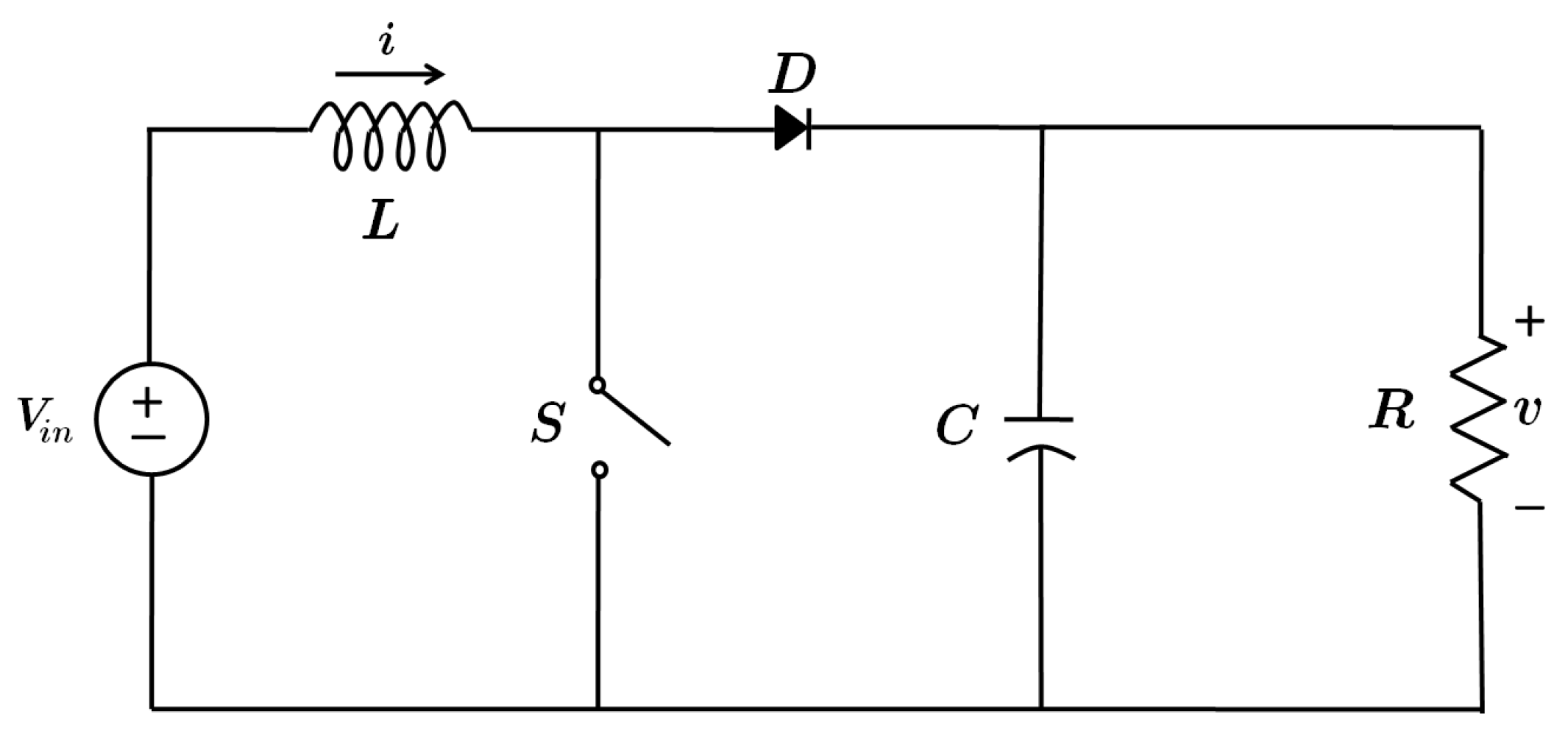
The control system that defines the boost converter is simplified, assuming that . Then, the basic scheme of a boost converter is displayed in Figure 1. In this figure, is the input voltage, i is the inductance current, L is the inductor, S is the switch, D is the diode, C is the capacitor, and v is the output voltage. When the switch S is closed (state ON), the coil L stores energy from the voltage source , while the load is fed by the capacitor C. In addition, when the switch is open (state OFF), the current can only pass through diode D and feed capacitor C and the load.
The boost converter is governed by the following differential equations:
Consequently, the state space in which the system evolves is a subset (where is a unit circle). Performing changes in system variables, the following expressions are obtained as presented in Equations (6)–(8).
The system shows a unique parameter in the following way:
A boost converter is a step-up power converter that obtains with . Therefore, when simulating the system, the initial voltage condition is assumed strictly to be more than 1. Now, Equations (10) and (11) are obtained when u changes in the set , as follows:
where:
This is a system with differential equations given by Equation (1), which can be written compactly as in Equation (15):
After considering each topology and calculating the exponential matrices, Equations (19) and (20) are obtained:
where is a two-by-two identity matrix.
In terms of each of the components, the solutions of the system presented in Equation (9) are as follows:
- For the topology 1 (),
- For the topology 2 (),where . Herein, an evaluation of must be considered to avoid unwanted solutions.
- If , Topology 3 is obtained as follows:
However, the discontinuous conduction mode presented in Topology 3 is not obtained in this paper and thus will be not evaluated.
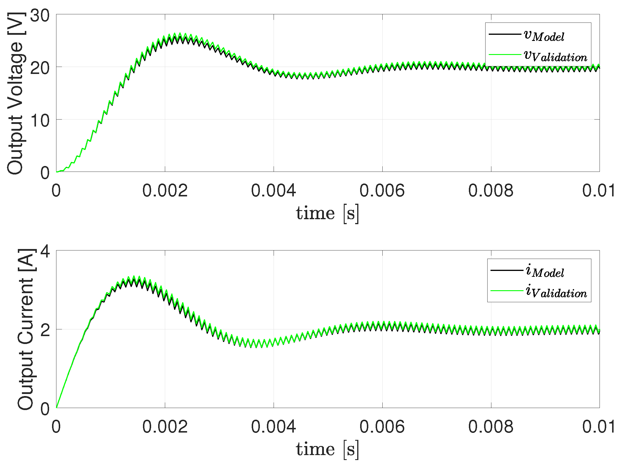
To validate the mathematical model described in (15), a more exact model is simulated in MATLAB where parameters of an experimental circuit are included, with the following parameters: V, , f, mH, , and . Herein, the term is the inductor internal resistance, and is the static drain-to-source on-resistance. The behavior in time of the open-loop system with a reference of V is shown in Figure 2. The results show that in both the transient state and steady-state operations, the two models behave similarly, concluding that Equation (15) is a good mathematical representation of the boost converter.
2.2. Pulse-Width Modulation
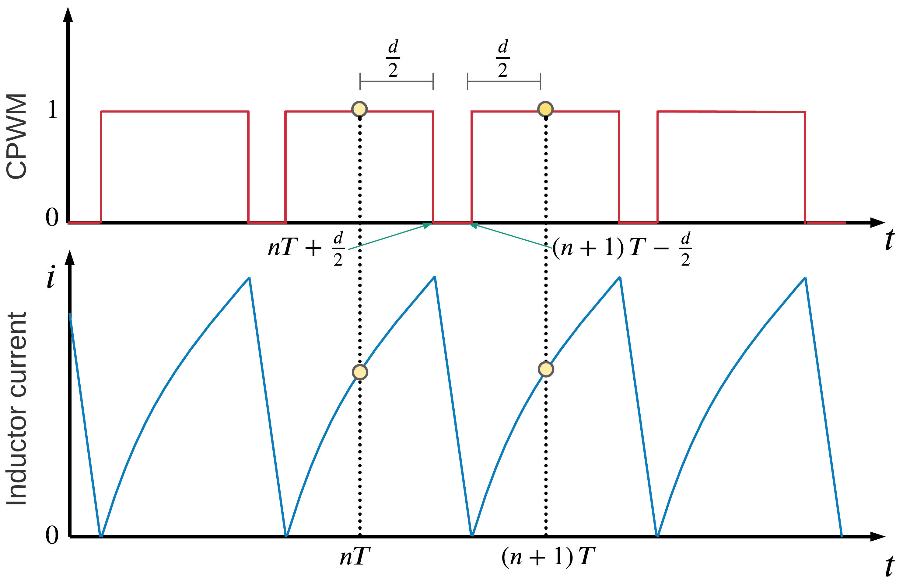
In this research, the CPWM is used. In period T, two commutations are made in such a way that a time interval is divided into three sub-intervals, where the first and last have the same length (Figure 3).
Switching is carried out according to the scheme . In general, the duty cycle varies from period to period due to continuous ON–OFF switching, where the traditional way of calculating the duty cycle d is by using a reference ramp.
2.3. Zero Average Dynamics Technique
The duty cycle is calculated with the ZAD technique, defining the time that the switch is open or closed. In this control technique, sampling is performed for the capacitor voltage (v) and the inductor current (i). These two variables are measured at and (where no transients are presented). The sampling process must be synchronized in such a way that all variables are measured simultaneously.
This technique consists of the following:
- Define the switching surface .
- Fix a period T.
- Force s to have zero average in each cycle (ZAD):
The last condition guarantees that only there will be a finite switching number per period, as the control was designed with that intention.
2.4. Piecewise Linear Approximation of the Switching Surface
As a CPWM is used, the control variable u that is applied to the system can be defined as follows:
The calculation of the duty cycle through Equation (28), implies the solution of a transcendent equation. A piecewise linear function is used to approximate the switching surface and to produce an elementary equation from which the duty cycle can be calculated analytically. Therefore, this approach is performed by considering the following assumptions [26]:
- The dynamics of the error or switching surface behaves like a piecewise linear function.
- The slopes of the dynamic error at each section are determined by the slopes calculated at the switching time, assuming that the slope at the beginning of the period, noted as , is the same as at the end. That means that in the sections between and , the slope of is , which corresponds to the derivative of the switching surface with respect to time for the case . Furthermore, in the section the slope of is and corresponds to the derivative of the switching surface with respect to time for the case .
Figure 4 shows the piecewise linear approximation of the switching surface.
From the assumptions and the figure presented above, the following mathematical expressions are obtained as shown in Equations (29)–(31):
To validate Equation (27), another approximation technique is selected. For instance, the Weierstrass approximation theorem states that for all real and continuous function f [27], defined in the compact interval , no degenerated and for each real number , there is a polynomial expression p that depends on the as follows:
for each . In other words, the function f can be approximated as uniform by the polynomial expression p. Therefore, choosing the as small as preferred, the relationship is established in Equation (27). Then, the following holds:
Indeed, from the triangular inequality is obtained the following:
and as follows:
Considering the following:
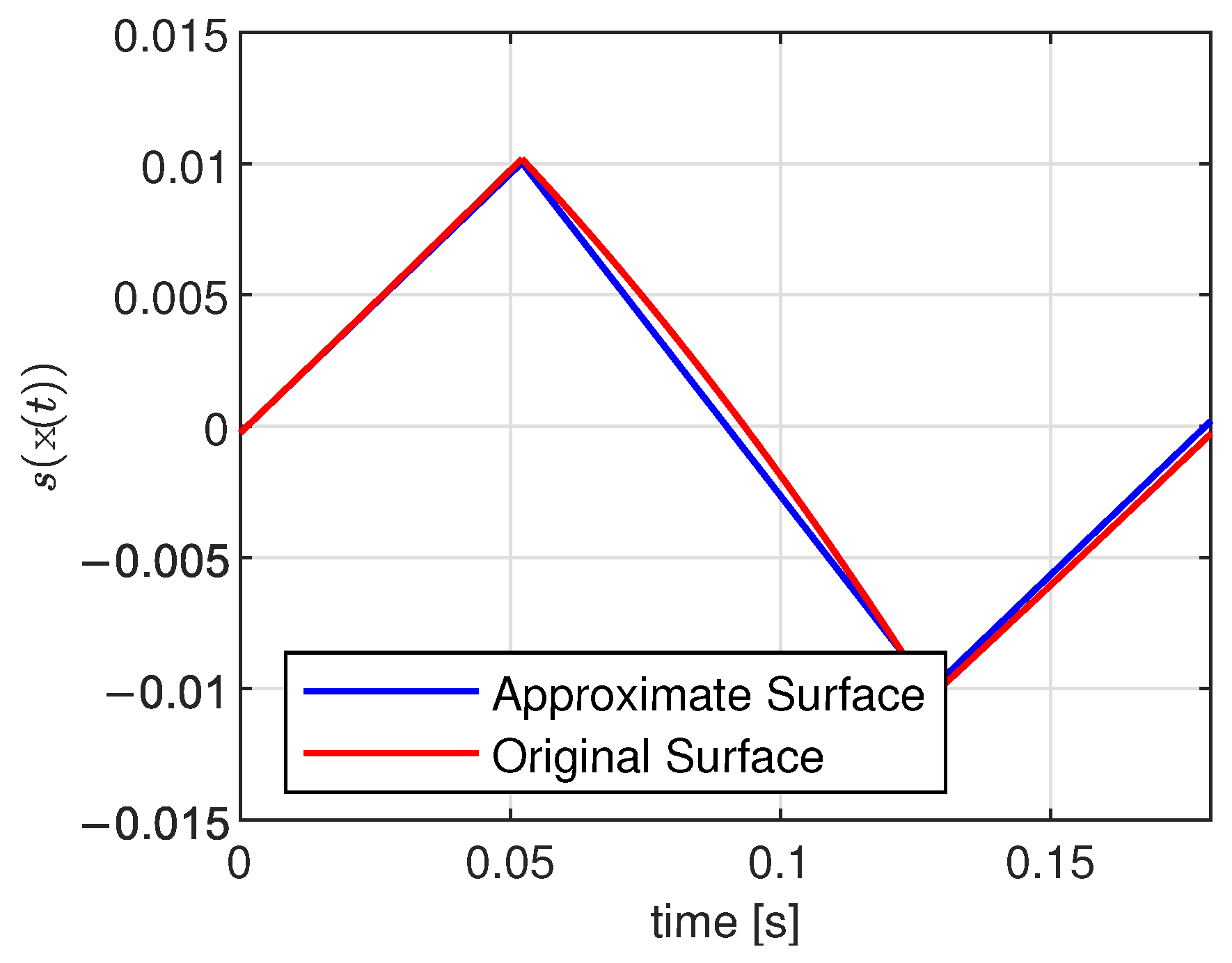
Despite this polynomial approximation, the problem that arises is when solving the duty cycle d from Equation (33). However, Figure 5 shows that the piecewise linear approximation of the switching surface is good.
Therefore, using the approximation of obtained with the piecewise linear technique, the following expression is obtained: , or the following:
Now, according to the different topologies, the following expressions are obtained:
- For Topology 1,
- For Topology 2,
Using the system solutions in each topology, considering the -periodic orbits; then the following holds:
- For Topology 1, given , if the following expression is chosen:then:
- For Topology 2, the following holds:with
Therefore, given , the following expression is chosen:
where . Now, the following expression is obtained:
The simulation of the system, implemented in MATLAB, shows that the approximation is good, and that it is better for the topology corresponding to than for .
Now, is the linear approximation of . For the topology , the following mathematical expression is obtained:
and it is null for , from which the maximum and minimum values occur at the extremes of the intervals (precisely at switching).
Now, we have the following:
A minimum value is obtained when and have the same signs, and a maximum value when and have opposite signs.
From Equation (49), it is obtained that and for , the maximum and minimum values obtained with the piecewise linear approximation of the switching surface depend on the switching instant .
2.5. Duty Cycle
The duty cycle is calculated using the ZAD technique by approximating the switching surface with a piecewise linear function and using the equality presented in Equation (27). Hence, using Equations (29)–(31) and the integral given by Equation (27), the following mathematical expression is obtained:
When equating to zero, the duty cycle (d) is then obtained as the following:
Values of the duty cycle could be or . In either of these two cases, the system saturates, even for the next election in each period. For instance, we have the following:
- If , the system is forced to evolve according to Topology 1.
- If , the system is forced to evolve according to Topology 2.
- If denominator of Equation (51), defined now as , is equal to zero, then two possibilities are defined: (a) the system is forced to evolve according to Topology 1 if the numerator ; (b) the system is forced to evolve according to Topology 2 if .
3. Results and Analysis
In this section, the performance of the ZAD technique is presented, considering voltage regulation and the presence of chaotic behavior. This analysis is performed by approximating the switching surface with a piecewise linear function.
3.1. ZAD with Piecewise Linear Approximation
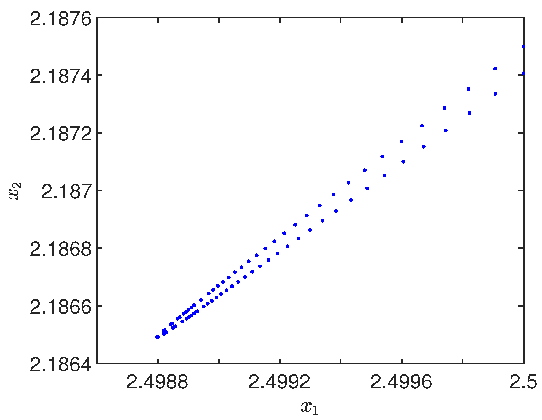
Figure 6 shows the state space of the system simulated with the constant parameters and . For each figure, , s, and are kept constant. Figure 6 shows that the system evolves to the stable fixed point of the Poincaré plot. This result shows the presence of periodic orbit in the dynamic system, defined in Equation (9). This simulation considers and .
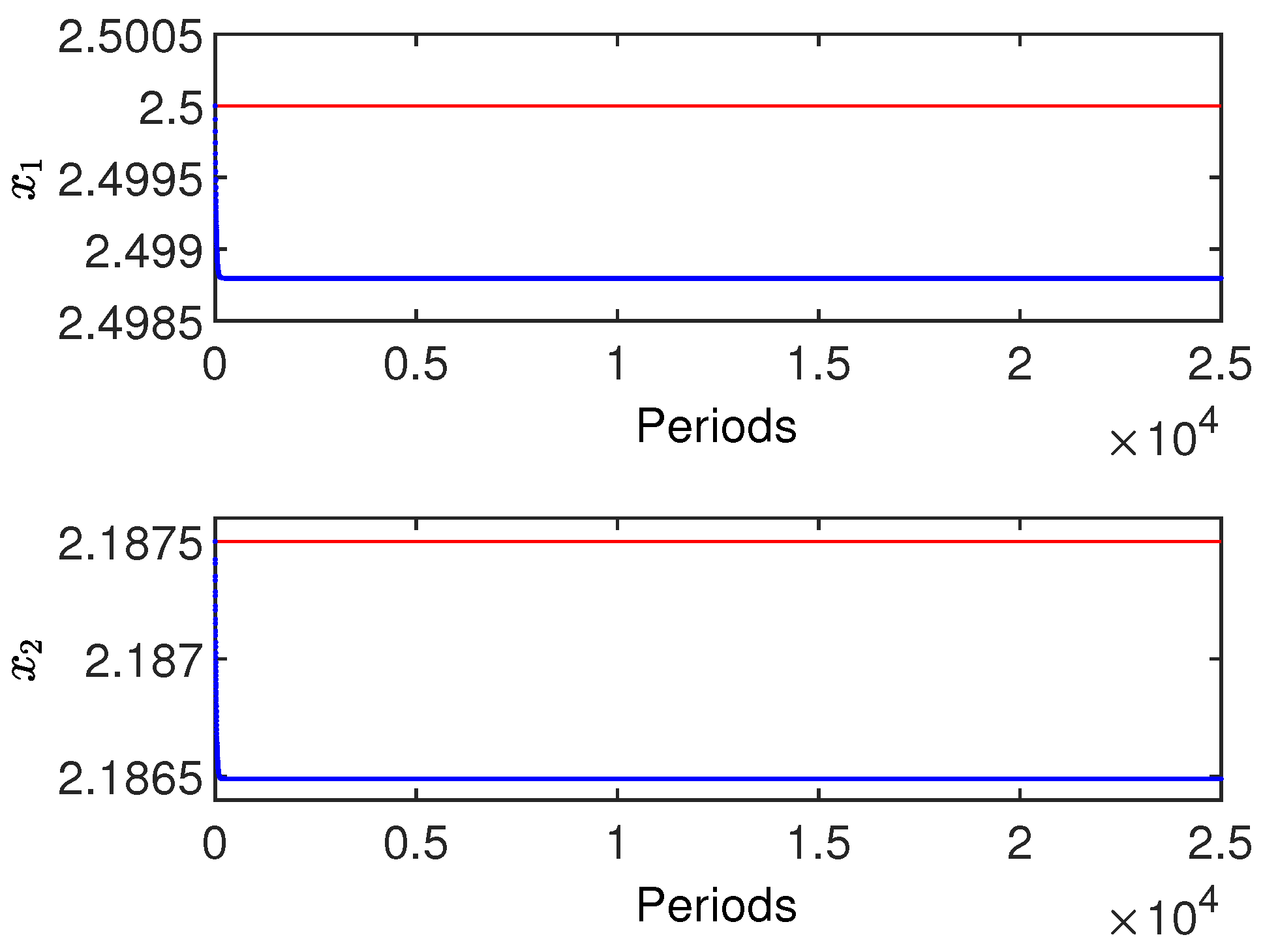
Figure 7 shows the regulation of the voltage and current variables, identified as and , respectively. The red lines correspond to the voltage and current references, and the blue lines are the measured variables. This simulation considers and . The result shows that the system presents excellent regulation in both current and voltage variables. The differences between the references and the measured values are obtained for the voltage as and the current as . These last calculations give a relative voltage regulation error of and a current regulation error of .
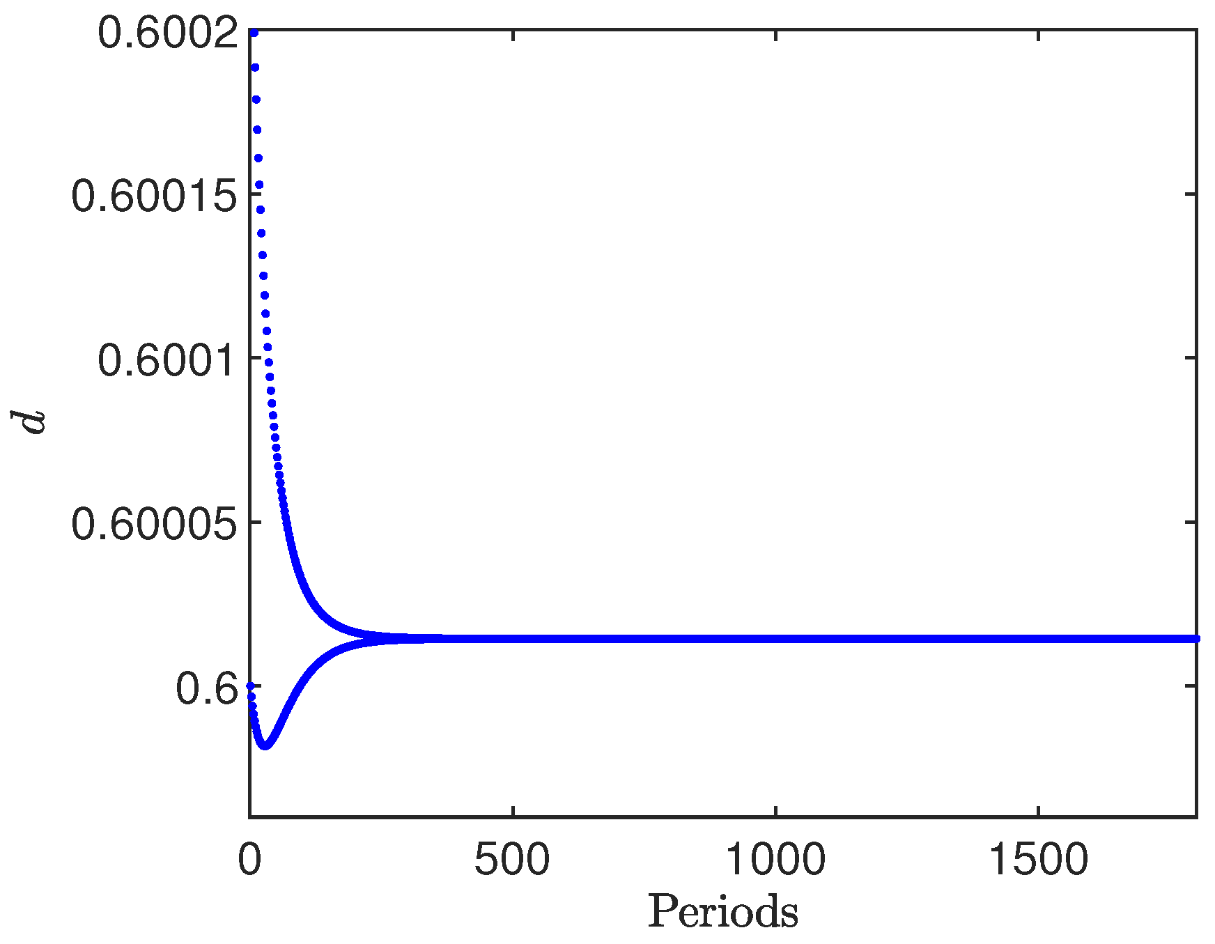
Figure 8 shows that the duty cycle stabilizes quickly at a value of . The duty cycle is normalized to changes between 0 and 1. This simulation considers and . In this case, the duty cycle is unsaturated and with fixed switching frequency [28], complying with the characteristics of this type of control presented in [5,23], which validates the veracity of these results.
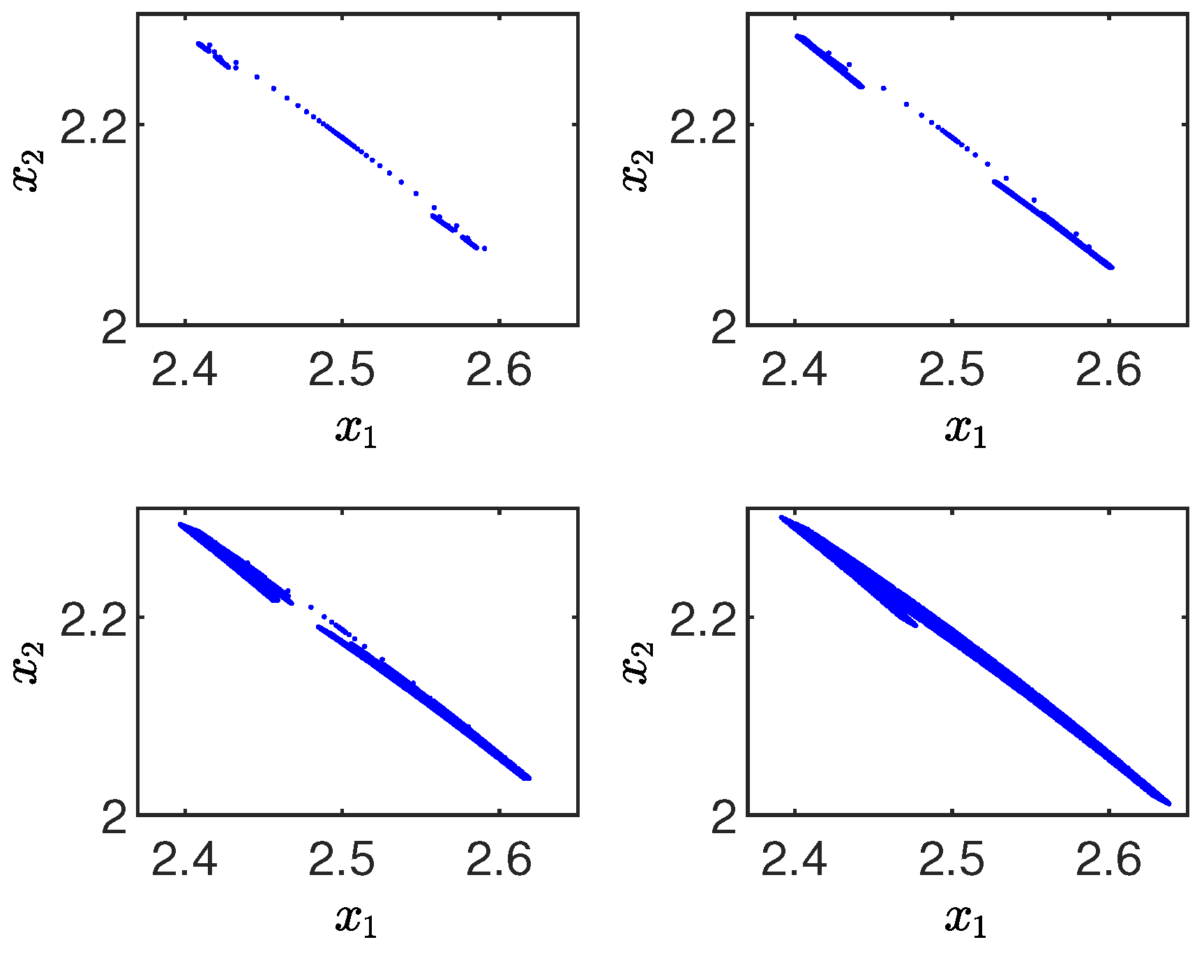
A chaotic attractor, identified with the letter A, is shown in Figure 9. For each graph in Figure 9, the following value is selected: . In the first figure, ; in the second, ; in the third, ; and in the last (corresponding to the attractor), the chosen value is . It is difficult to find the exact value of that causes a chaotic attractor.
Figure 10 corresponds to an extension of the chaotic attractor. Note that as a subset of the state space, the attractor A is contained, for example, in the ball centered at and radius 1, which means that A is bounded.
This figure shows the first iteration of the Poincaré map and iterations from 14,930 to 14,935 corresponding to an initial condition , which is close to or the set A. In addition, it is observed that these iterations oscillate without a certain pattern. Set A has a sensitive dependence on the initial conditions [29].
Using the Euclidean metric, the distance between the previous iterations and set A is estimated. This distance is less than (where u represents the units) and it is calculated by constructing a perpendicular line to the set A and passing through the point corresponding to iteration 14,932. Then, a right triangle is constructed with a vertex in this iteration and hypotenuse in the perpendicular line. Numerically, set A attracts from a certain iteration all the iterations that follow. The generation of set A is carried out with 30,000 iterations of the Poincaré map.
Choosing other initial conditions close to , the result shows that set A is indeed a chaotic attractor. Then, with the calculation of the Lyapunov exponents, A is found in an area where the system exhibits chaotic behavior. Figure 11 shows that, even though it operates in a chaotic regime, the system presents good regulation in both the voltage and current. Indeed, and . The relative voltage error of and the relative current error of are obtained.
The scattered points in Figure 12 correspond to the evolution of the duty cycle, and they confirm that the system is operating in a chaotic regime.
3.2. Regulation
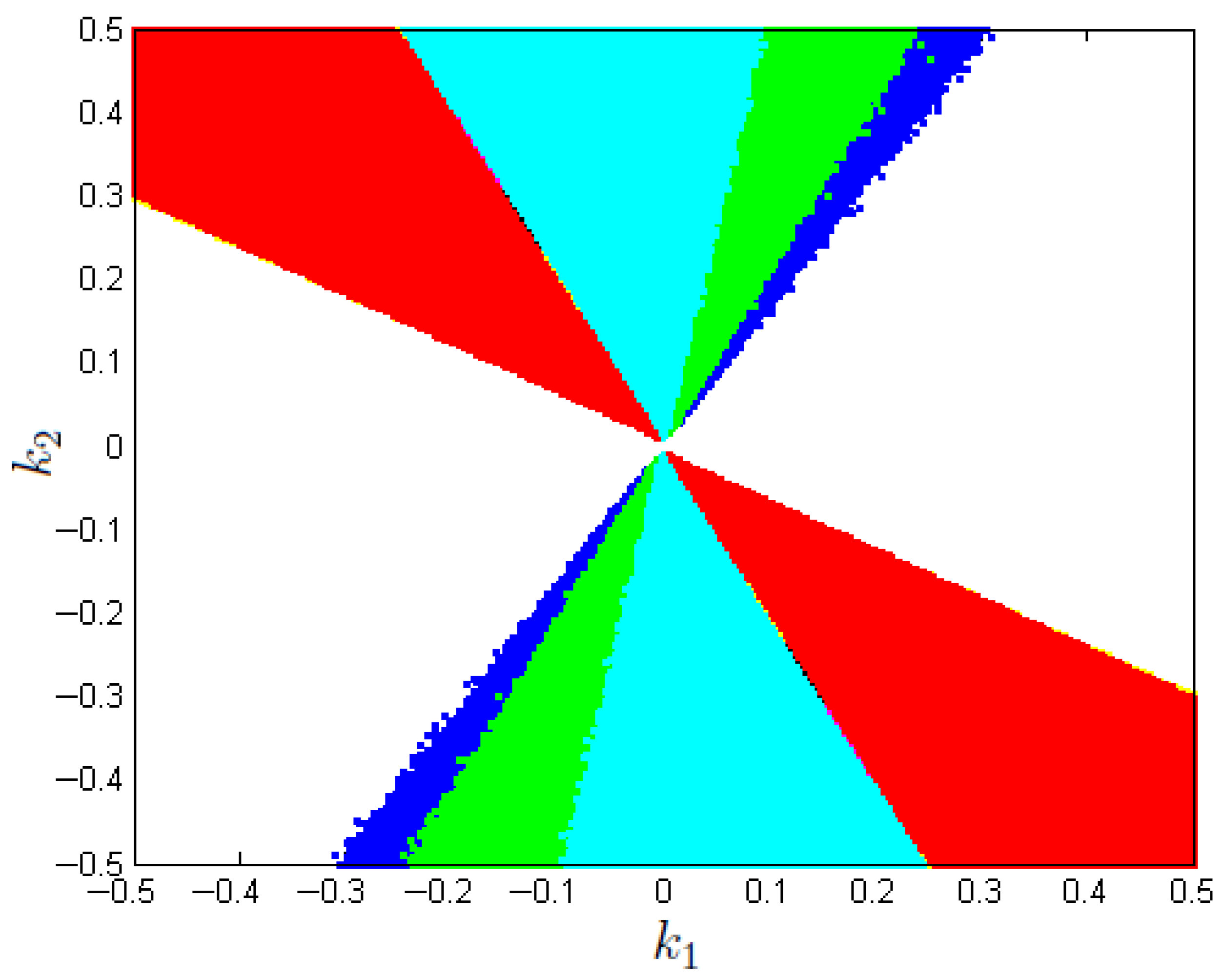
This section analyzes the ability of the ZAD and boost converter to follow a constant reference signal (system regulation) with changes in the switching surface parameters ). Hence, Figure 13 shows different regulation zones in the bi-parametric space diagram graphed in the planes and . These results show that the system regulates the voltage magnitude from to . The reference signal to follow is constant and equal to .
The regulation error is greater than in the white zones, which means that the operation is not good. Furthermore, in the blue zones, the regulation error is ; in the green zones, it is ; and in the cyan zones, it is . Moreover, in the magenta zones, the regulation error is ; in the black zones, it is ; in the yellow zones, it is ; and in the red zones, it is . Therefore, these results show a wide area where the system is regulating well with errors from to .
4. Conclusions
This paper presents the performance of a boost converter with a ZAD control technique to regulate DC signals. The boost converter system was modeled in a compact form and a variable change was performed to depend only on the parameter. A new switching surface was proposed, where it is possible to regulate both the voltage and the current variables with low relative errors with respect to the reference signals. It was analytically demonstrated that the piecewise linear approximation of the switching surface is an efficient technique to control the system. Moreover, it was shown numerically that the system evolved into a chaotic attractor for certain operating conditions. Finally, the results showed that the ZAD technique implemented in the boost converter has good regulation, as in the bi-parametric space × , the system can operate in zones that present regulation errors from 1% to 7%.
Author Contributions
Conceptualization, investigation, methodology, and software, S.C.T. Formal analysis, writing—review, and editing, S.C.T., J.E.C.-B. and F.E.H. All authors have read and agreed to the published version of the manuscript.
Funding
This research received no external funding.
Institutional Review Board Statement
Not applicable.
Informed Consent Statement
Not applicable.
Data Availability Statement
Not applicable.
Acknowledgments
The work of Simeón Casanova Trujillo was supported by Universidad Nacional de Colombia, Sede Manizales. The work of F.E.H. and J.E.C.-B. was supported by Universidad Nacional de Colombia, Sede Medellín.
Conflicts of Interest
The authors declare no conflict of interest.
References
- Buso, S.; Mattavelli, P. Digital Control in Power Electronics; Morgan and Claypool Publishers: San Rafael, CA, USA, 2015. [Google Scholar]
- Forouzesh, M.; Shen, Y.; Yari, K.; Siwakoti, Y.P.; Blaabjerg, F. High-Efficiency High Step-Up DC–DC Converter With Dual Coupled Inductors for Grid-Connected Photovoltaic Systems. IEEE Trans. Power Electron. 2018, 33, 5967–5982. [Google Scholar] [CrossRef]
- Bilalovic, F.; Music, O.; Sabanovic, A. Buck converter regulator operating in the sliding mode. In Proceedings of the VII International PCI, Orlando, FL, USA, 19–21 April 1983; pp. 331–340. [Google Scholar]
- Carpita, M.; Marchesoni, M.; Oberti, M.; Puglisi, L. Power conditioning system using sliding model control. In Proceedings of the PESC ’88 Record, 19th Annual IEEE Power Electronics Specialists Conference, Kyoto, Japan, 11–14 April 1988; pp. 626–633. [Google Scholar] [CrossRef]
- Fossas, E.; Griño, R.; Biel, D. Quasi-sliding control based on pulse width modulation, zero averaged dynamics and the L2 norm. In Advances in Variable Structure Systems; World Scientific: Singapore, 2000; pp. 335–344. [Google Scholar] [CrossRef]
- Repecho, V.; Biel, D.; Ramos-Lara, R.; Vega, P.G. Fixed-Switching Frequency Interleaved Sliding Mode Eight-Phase Synchronous Buck Converter. IEEE Trans. Power Electron. 2018, 33, 676–688. [Google Scholar] [CrossRef] [Green Version]
- Hoyos, F.E.; Candelo-Becerra, J.E.; Rincón, A. Zero Average Dynamic Controller for Speed Control of DC Motor. Appl. Sci. 2021, 11, 5608. [Google Scholar] [CrossRef]
- Hoyos, F.E.; Candelo-Becerra, J.E.; Hoyos Velasco, C.I. Model-Based Quasi-Sliding Mode Control with Loss Estimation Applied to DC–DC Power Converters. Electronics 2019, 8, 1086. [Google Scholar] [CrossRef] [Green Version]
- Zhou, G.; Mao, S.; Zhou, S.; Wang, Y.; Yan, T. Discrete-Time Modeling and Symmetrical Dynamics of V2-Controlled Buck Converters With Trailing-Edge and Leading-Edge Modulations. IEEE J. Emerg. Sel. Top. Power Electron. 2020, 8, 3995–4008. [Google Scholar] [CrossRef]
- Singha, A.K.; Kapat, S.; Banerjee, S.; Pal, J. Nonlinear Analysis of Discretization Effects in a Digital Current Mode Controlled Boost Converter. IEEE J. Emerg. Sel. Top. Circuits Syst. 2015, 5, 336–344. [Google Scholar] [CrossRef]
- Fossas, E.; Olivar, G. Study of chaos in the buck converter. IEEE Trans. Circuits Syst. Fundam. Theory Appl. 1996, 43, 13–25. [Google Scholar] [CrossRef] [Green Version]
- di Bernardo, M.; Garefalo, F.; Glielmo, L.; Vasca, F. Switchings, bifurcations, and chaos in DC/DC converters. IEEE Trans. Circuits Syst. Fundam. Theory Appl. 1998, 45, 133–141. [Google Scholar] [CrossRef]
- Hu, W.; Zhang, B.; Yang, R. Bifurcation Mechanism and Stabilization of V2C Controlled Buck Converter. IEEE Access 2019, 7, 77174–77182. [Google Scholar] [CrossRef]
- Baillieul, J.; Brockett, R.; Washburn, R. Chaotic motion in nonlinear feedback systems. IEEE Trans. Circuits Syst. 1980, 27, 990–997. [Google Scholar] [CrossRef]
- Zhang, X.; Xu, J.; Bao, B.; Zhou, G. Asynchronous-Switching Map-Based Stability Effects of Circuit Parameters in Fixed Off-Time Controlled Buck Converter. IEEE Trans. Power Electron. 2016, 31, 6686–6697. [Google Scholar] [CrossRef]
- Deane, J.; Hamill, D. Analysis, simulation and experimental study of chaos in the buck converter. In Proceedings of the 21st Annual IEEE Conference on Power Electronics Specialists, San Antonio, TX, USA, 11–14 June 1990; pp. 491–498. [Google Scholar] [CrossRef]
- Tse, C.K. Complex Behavior of Switching Power Converters (Power Electronics and Applications); CRC Press: New York, NY, USA, 2004; p. 266. [Google Scholar]
- Banerjee, S.; Verghese, G.C. Nonlinear Phenomena in Power Electronics; Wiley-IEEE Press: Hoboken, NJ, USA, 2001; p. 472. [Google Scholar]
- Amador, A.; Casanova, S.; Granada, H.A.; Olivar, G.; Hurtado, J. Codimension-Two Big-Bang Bifurcation in a ZAD-Controlled Boost DC-DC Converter. Int. J. Bifurc. Chaos 2014, 24, 1450150. [Google Scholar] [CrossRef]
- Vergara Perez, D.D.C.; Trujillo, S.C.; Hoyos Velasco, F.E. Period Addition Phenomenon and Chaos Control in a ZAD Controlled Boost Converter. Int. J. Bifurc. Chaos 2018, 28, 1850157. [Google Scholar] [CrossRef]
- Perez, D.D.C.V.; Trujillo, S.C.; Hoyos Velasco, F.E. On the dynamic behavior of the current in the condenser of a boost converter controlled with ZAD. TELKOMNIKA (Telecommun. Comput. Electron. Control) 2020, 18, 1678. [Google Scholar] [CrossRef]
- Munoz, J.; Osorio, G.; Angulo, F. Boost converter control with ZAD for power factor correction based on FPGA. In Proceedings of the 2013 Workshop on Power Electronics and Power Quality Applications (PEPQA), Bogota, Colombia, 6–7 July 2013; pp. 1–5. [Google Scholar] [CrossRef]
- Repecho, V.; Biel, D.; Ramos-Lara, R. Robust ZAD Sliding Mode Control for an 8-Phase Step-Down Converter. IEEE Trans. Power Electron. 2020, 35, 2222–2232. [Google Scholar] [CrossRef]
- Baumaister, J.; Leitão, A. Introdução à Teoria de Controle e Programação Dinâmica; Instituto Nacional de Matemática Pura e Aplicada: Rio de Janeiro, Brazil, 2014; p. 399. [Google Scholar]
- Doering, C.I.; Lopes, A.O. Equacoes Diferenciais Ordinárias; Instituto Nacional de Matemática Pura e Aplicada: Rio de Janeiro, Brazil, 2016; p. 423. [Google Scholar]
- Angulo García, F. Análisis de la Dinámica de Convertidores Electrónicos de Potencia Usando PWM Basado en Promediado Cero de la Dinámica del Error (ZAD). Ph.D. Thesis, Universitat Polytècnica de Catalunya, Barcelona, Spain, 2004. [Google Scholar]
- Apostol, T.M. Análisis Matemático, 2nd ed.; Editorial Reverté: Barcelona, Spain, 1977; p. 596. [Google Scholar]
- Hoyos Velasco, F.E.; Toro-García, N.; Garcés Gómez, Y.A. Adaptive Control for Buck Power Converter Using Fixed Point Inducting Control and Zero Average Dynamics Strategies. Int. J. Bifurc. Chaos 2015, 25, 1550049. [Google Scholar] [CrossRef]
- Gulick, D. Encounters With Chaos, 1st ed.; McGraw-Hill College: New York, NY, USA, 1992; p. 244. [Google Scholar]
Figure 1.
Simplified diagram of the boost converter.

Figure 2.
Validation of the mathematical model proposed in Equation (15).
Figure 2.
Validation of the mathematical model proposed in Equation (15).

Figure 3.
Symmetrical centered pulse-width modulation.

Figure 4.
Piecewise linear approximation of the switching surface.

Figure 5.
Original surface vs. piecewise linear approximation.

Figure 6.
State space.

Figure 7.
Behavior of the voltage and current regulation.

Figure 8.
Evolution of the duty cycle.

Figure 9.
Birth of a chaotic attractor.

Figure 10.
State space.

Figure 11.
Behavior of the regulation.

Figure 12.
Evolution of the duty cycle.

Figure 13.
Bi-parametric diagram for regulation.

Publisher’s Note: MDPI stays neutral with regard to jurisdictional claims in published maps and institutional affiliations. |
© 2021 by the authors. Licensee MDPI, Basel, Switzerland. This article is an open access article distributed under the terms and conditions of the Creative Commons Attribution (CC BY) license (https://creativecommons.org/licenses/by/4.0/).
Share and Cite
MDPI and ACS Style
Trujillo, S.C.; Candelo-Becerra, J.E.; Hoyos, F.E. Performance of the Boost Converter Controlled with ZAD to Regulate DC Signals. Computation 2021, 9, 96. https://0-doi-org.brum.beds.ac.uk/10.3390/computation9090096
AMA Style
Trujillo SC, Candelo-Becerra JE, Hoyos FE. Performance of the Boost Converter Controlled with ZAD to Regulate DC Signals. Computation. 2021; 9(9):96. https://0-doi-org.brum.beds.ac.uk/10.3390/computation9090096
Chicago/Turabian StyleTrujillo, Simeón Casanova, John E. Candelo-Becerra, and Fredy E. Hoyos. 2021. "Performance of the Boost Converter Controlled with ZAD to Regulate DC Signals" Computation 9, no. 9: 96. https://0-doi-org.brum.beds.ac.uk/10.3390/computation9090096
Note that from the first issue of 2016, this journal uses article numbers instead of page numbers. See further details here.