Unconventional Applications of Superconducting Nanowire Single Photon Detectors

 and
and 
Abstract
:1. Introduction
2. SNSPD Concept Origins, Operation and Metrics
3. Non-Standard Photo-Detection Techniques
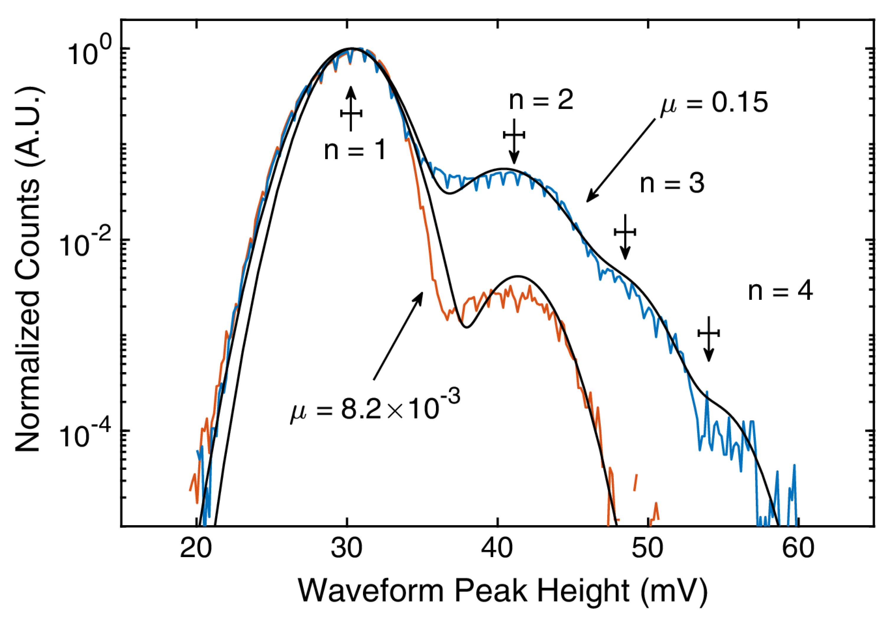
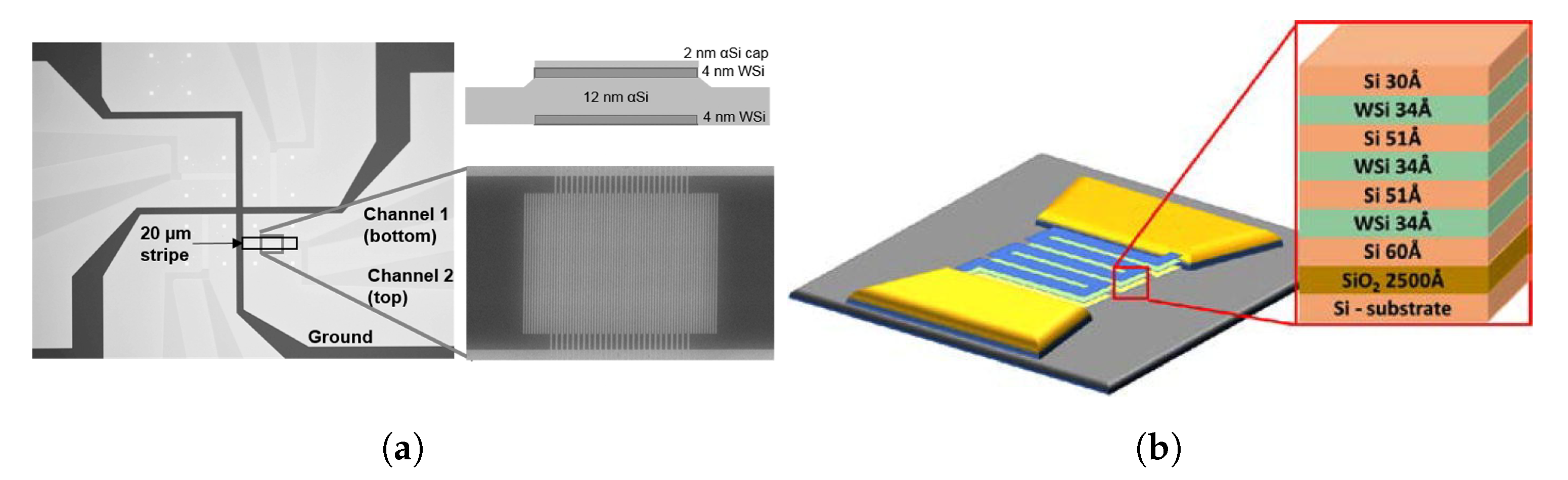
3.1. Multi-Photon Detection and Multi-Layer Broadband SNSPDs
3.2. Detection in Strong Magnetic Fields
4. Particle Detection
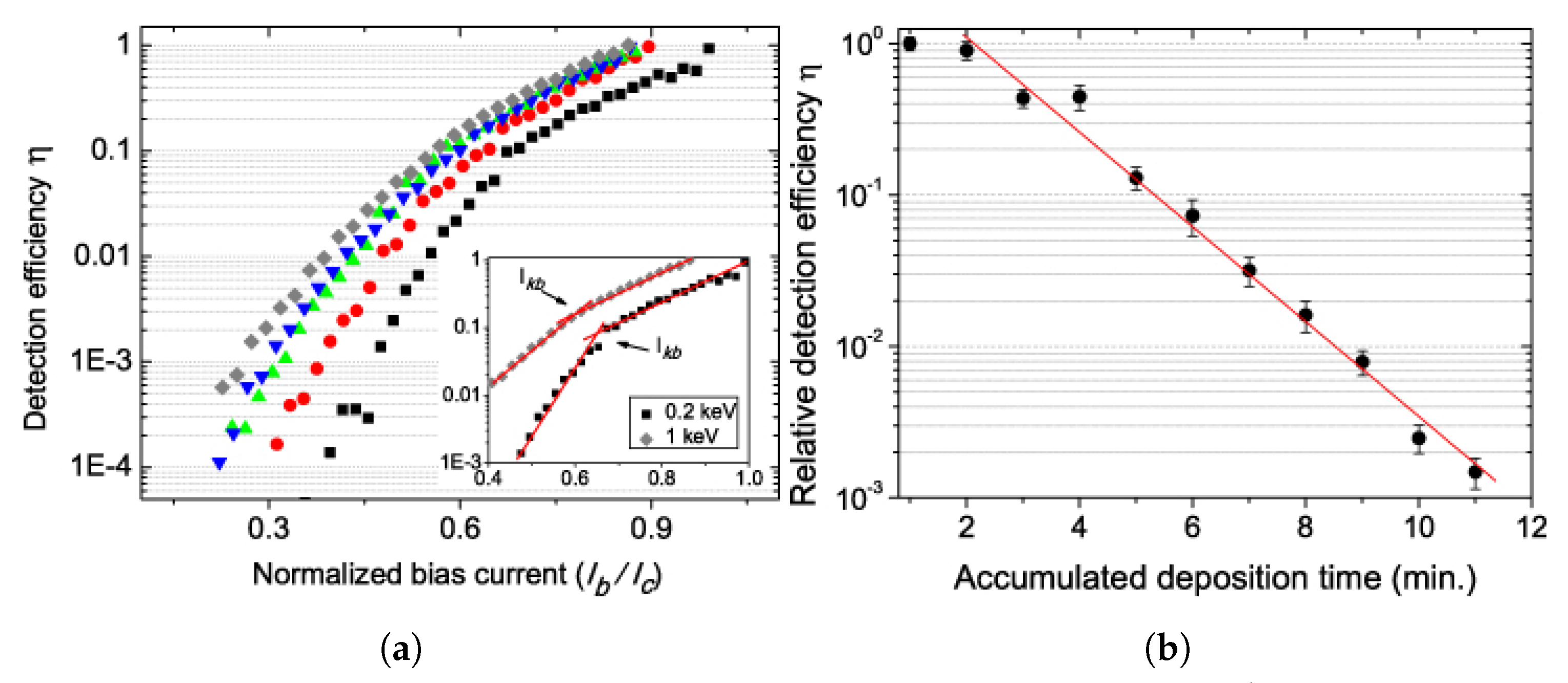
4.1. Low Energy Ion Detection
4.2. Low Energy Electron Detection
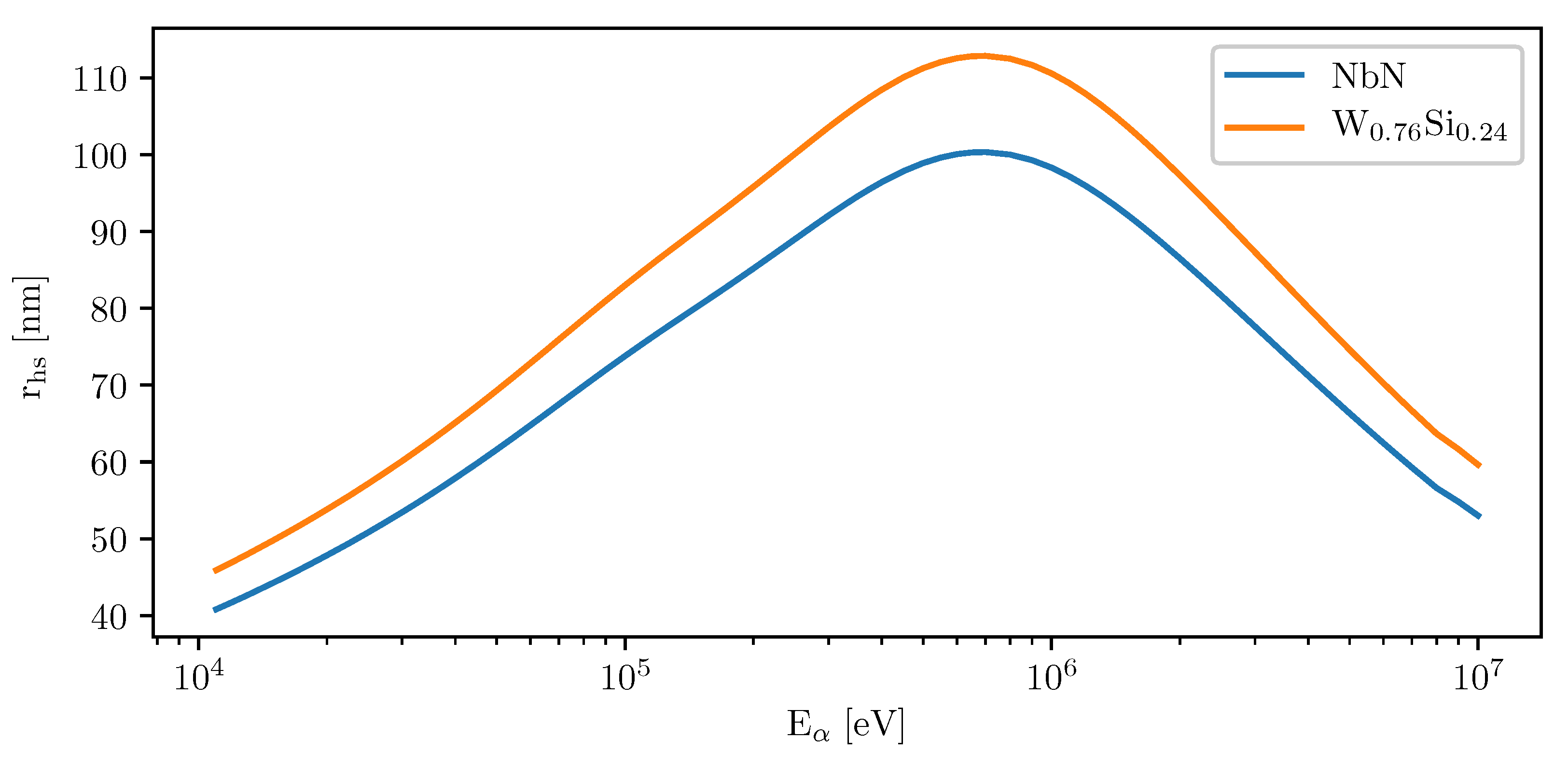
4.3. High Energy Particle Detection
4.4. Neutron and Dark Matter Detection
5. Conclusions
Author Contributions
Funding
Conflicts of Interest
References
- Gol’Tsman, G.; Okunev, O.; Chulkova, G.; Lipatov, A.; Semenov, A.; Smirnov, K.; Voronov, B.; Dzardanov, A.; Williams, C.; Sobolewski, R. Picosecond superconducting single-photon optical detector. Appl. Phys. Lett. 2001, 79, 705–707. [Google Scholar] [CrossRef]
- Wu, J.; You, L.; Chen, S.; Li, H.; He, Y.; Lv, C.; Wang, Z.; Xie, X. Improving the timing jitter of a superconducting nanowire single-photon detection system. Appl. Opt. 2017, 56, 2195–2200. [Google Scholar] [CrossRef] [PubMed]
- Marsili, F.; Verma, V.B.; Stern, J.A.; Harrington, S.; Lita, A.E.; Gerrits, T.; Vayshenker, I.; Baek, B.; Shaw, M.D.; Mirin, R.P.; et al. Detecting single infrared photons with 93% system efficiency. Nat. Photonics 2013, 7, 210. [Google Scholar] [CrossRef]
- Zhang, W.; You, L.; Li, H.; Huang, J.; Lv, C.; Zhang, L.; Liu, X.; Wu, J.; Wang, Z.; Xie, X. NbN superconducting nanowire single photon detector with efficiency over 90% at 1550 nm wavelength operational at compact cryocooler temperature. Sci. China Phys. Mech. Astron. 2017, 60, 120314. [Google Scholar] [CrossRef] [Green Version]
- Shibata, H.; Shimizu, K.; Takesue, H.; Tokura, Y. Ultimate low system dark-count rate for superconducting nanowire single-photon detector. Opt. Lett. 2015, 40, 3428–3431. [Google Scholar] [CrossRef]
- Zhu, J.; Chen, Y.; Zhang, L.; Jia, X.; Feng, Z.; Wu, G.; Yan, X.; Zhai, J.; Wu, Y.; Chen, Q.; et al. Demonstration of measuring sea fog with an SNSPD-based Lidar system. Sci. Rep. 2017, 7, 1–7. [Google Scholar] [CrossRef] [Green Version]
- Takesue, H.; Dyer, S.D.; Stevens, M.J.; Verma, V.; Mirin, R.P.; Nam, S.W. Quantum teleportation over 100 km of fiber using highly efficient superconducting nanowire single-photon detectors. Optica 2015, 2, 832–835. [Google Scholar] [CrossRef] [Green Version]
- Takesue, H.; Nam, S.W.; Zhang, Q.; Hadfield, R.H.; Honjo, T.; Tamaki, K.; Yamamoto, Y. Quantum key distribution over a 40-dB channel loss using superconducting single-photon detectors. Nat. Photonics 2007, 1, 343. [Google Scholar] [CrossRef] [Green Version]
- Chen, J.; Altepeter, J.B.; Medic, M.; Lee, K.F.; Gokden, B.; Hadfield, R.H.; Nam, S.W.; Kumar, P. Demonstration of a quantum controlled-NOT gate in the telecommunications band. Phys. Rev. Lett. 2008, 100, 133603. [Google Scholar] [CrossRef] [Green Version]
- Natarajan, C.M.; Tanner, M.G.; Hadfield, R.H. Superconducting nanowire single-photon detectors: Physics and applications. Supercond. Sci. Technol. 2012, 25, 063001. [Google Scholar] [CrossRef]
- Hewett, J.; Weerts, H.; Brock, R.; Butler, J.; Casey, B.; Collar, J.; de Gouvea, A.; Essig, R.; Grossman, Y.; Haxton, W.; et al. Fundamental physics at the intensity frontier. arXiv 2012, arXiv:1205.2671. [Google Scholar]
- Bull, P.; Fitzgerald, J.; Harris, R.; Gunarathne, D.; Kaczanowics, E.; Kraishan, A.; Li, X.; McCormick, M.; Meziani, Z.; Miller, G.; et al. Design and Assembly of Fast and Lightweight Barrel and Forward Tracking Prototype Systems for an EIC. Available online: https://wiki.bnl.gov/conferences/images/7/78/EIC-RD2013-3-Status-Proposal-Saclay-TU.pdf (accessed on 18 May 2020).
- Niinikoski, T.; Abreu, M.; Anbinderis, P.; Anbinderis, T.; D’Ambrosio, N.; De Boer, W.; Borchi, E.; Borer, K.; Bruzzi, M.; Buontempo, S.; et al. Low-temperature tracking detectors. Nuclear Instrum. Methods Phys. Res. Sect. A Accel. Spectrom. Detect. Assoc. Equip. 2004, 520, 87–92. [Google Scholar] [CrossRef]
- Abelev, B.; Adam, J.; Adamová, D.; Aggarwal, M.; Rinella, G.A.; Agnello, M.; Agostinelli, A.; Agrawal, N.; Ahammed, Z.; Ahmad, N.; et al. Technical design report for the upgrade of the ALICE inner tracking system. J. Phys. G Nucl. Part. Phys. 2014, 41, 087002. [Google Scholar] [CrossRef] [Green Version]
- Adare, A.; Aidala, C.; Ajitanand, N.; Akiba, Y.; Akimoto, R.; Alfred, M.; Apadula, N.; Aramaki, Y.; Asano, H.; Atomssa, E.; et al. Concept for an Electron Ion Collider (EIC) detector built around the BaBar solenoid. arXiv 2014, arXiv:1402.1209. [Google Scholar]
- Khalek, S.A.; Allongue, B.; Anghinolfi, F.; Barrillon, P.; Blanchot, G.; Blin-Bondil, S.; Braem, A.; Chytka, L.; Muino, P.C.; Düren, M.; et al. The ALFA roman pot detectors of ATLAS. J. Instrum. 2016, 11, P11013. [Google Scholar] [CrossRef] [Green Version]
- Bültmann, S.; Chen, W.; Chiang, I.; Chrien, R.; Drees, A.; Gill, R.; Guryn, W.; Landgraf, J.; Li, Z.; Ljubicic, T.; et al. The PP2PP experiment at RHIC: Silicon detectors installed in Roman Pots for forward proton detection close to the beam. Nucl. Instrum. Methods Phys. Res. Sect. A Accel. Spectrom. Detect. Assoc. Equip. 2004, 535, 415–420. [Google Scholar] [CrossRef]
- Ruggiero, G.; Avati, V.; Antchev, G.; Deile, M.; Eggert, K.; Eremin, V.; Kaspar, J.; Niewiadomski, H.; Petäjäjärvi, J.; Radicioni, E.; et al. Characteristics of edgeless silicon detectors for the Roman Pots of the TOTEM experiment at the LHC. Nucl. Instrum. Methods Phys. Res. Sect. A Accel. Spectrom. Detect. Assoc. Equip. 2009, 604, 242–245. [Google Scholar] [CrossRef]
- Polakovic, T.; Armstrong, W.; Yefremenko, V.; Pearson, J.; Hafidi, K.; Karapetrov, G.; Meziani, Z.E.; Novosad, V. Superconducting nanowires as high-rate photon detectors in strong magnetic fields. Nucl. Instrum. Methods Phys. Res. Sect. A Accel. Spectrom. Detect. Assoc. Equip. 2020, 959, 163543. [Google Scholar] [CrossRef] [Green Version]
- Testardi, L. Destruction of superconductivity by laser light. Phys. Rev. B 1971, 4, 2189. [Google Scholar] [CrossRef]
- Shklovskij, V. Hot electrons in metal films at low temperatures. Low Temp. Phys. 2018, 44, 165–183. [Google Scholar] [CrossRef]
- Semenov, A.; Nebosis, R.; Gousev, Y.P.; Heusinger, M.; Renk, K. Analysis of the nonequilibrium photoresponse of superconducting films to pulsed radiation by use of a two-temperature model. Phys. Rev. B 1995, 52, 581. [Google Scholar] [CrossRef] [PubMed]
- Gershenzon, E.; Gol’tsman, G.; Semenov, A.; Sergeev, A. Mechanism of picosecond response of granular YBaCuO films to electromagnetic radiation. Solid State Commun. 1990, 76, 493–497. [Google Scholar] [CrossRef]
- Sergeev, A. Nonselective effect of electromagnetic radiation on a superconducting film in the resistive state. JETP Lett. 1982, 36, 244. [Google Scholar]
- Maneval, J.P.; Chibane, F.; Bland, R. Electron-phonon decoupling in the photoresponse of YBaCuO granular films at low temperature. Appl. Phys. Lett. 1992, 61, 339–341. [Google Scholar] [CrossRef]
- Perrin, N.; Vanneste, C. Response of superconducting films to a periodic optical irradiation. Phys. Rev. B 1983, 28, 5150. [Google Scholar] [CrossRef]
- Frenkel, A. Mechanism of nonequilibrium optical response of high-temperature superconductors. Phys. Rev. B 1993, 48, 9717. [Google Scholar] [CrossRef]
- Gol’Tsman, G.; Semenov, A.; Gousev, Y.P.; Zorin, M.; Godidze, I.; Gershenzon, E.; Lang, P.; Knott, W.; Renk, K. Sensitive picosecond NbN detector for radiation from millimetre wavelengths to visible light. Supercond. Sci. Technol. 1991, 4, 453. [Google Scholar] [CrossRef]
- Lindgren, M.; Currie, M.; Zeng, W.S.; Sobolewski, R.; Cherednichenko, S.; Voronov, B.; Gol’tsman, G. Picosecond response of a superconducting hot-electron NbN photodetector. Appl. Supercond. 1998, 6, 423–428. [Google Scholar] [CrossRef]
- Skocpol, W.; Beasley, M.; Tinkham, M. Self-heating hotspots in superconducting thin-film microbridges. J. Appl. Phys. 1974, 45, 4054–4066. [Google Scholar] [CrossRef]
- Bremer, J.W.; Newhouse, V. Thermal propagation effect in thin superconducting films. Phys. Rev. Lett. 1958, 1, 282. [Google Scholar] [CrossRef]
- Broom, R.; Rhoderick, E. A New Type of Bistable Element Involving Thermal Propagation of a Normal Region in a Thin Superconducting Film; Office of Naval Research, Department of the Navy: Arlington, VA, USA, 1960; p. 113. [Google Scholar]
- Broom, R.; Rhoderick, E. Thermal propagation of a normal region in a thin superconducting film and its application to a new type of bistable element. Br. J. Appl. Phys. 1960, 11, 292. [Google Scholar] [CrossRef]
- Cherry, W.; Gittleman, J. Thermal and electrodynamic aspects of the superconductive transition process. Solid-State Electron. 1960, 1, 287–305. [Google Scholar] [CrossRef]
- Kadin, A.; Johnson, M. Nonequilibrium photon-induced hotspot: A new mechanism for photodetection in ultrathin metallic films. Appl. Phys. Lett. 1996, 69, 3938–3940. [Google Scholar] [CrossRef]
- Semenov, A.D.; Gol’tsman, G.N.; Korneev, A.A. Quantum detection by current carrying superconducting film. Phys. C Supercond. 2001, 351, 349–356. [Google Scholar] [CrossRef]
- Il’in, K.; Lindgren, M.; Currie, M.; Semenov, A.; Gol’Tsman, G.; Sobolewski, R.; Cherednichenko, S.; Gershenzon, E. Picosecond hot-electron energy relaxation in NbN superconducting photodetectors. Appl. Phys. Lett. 2000, 76, 2752–2754. [Google Scholar] [CrossRef] [Green Version]
- Vodolazov, D.Y. Single-photon detection by a dirty current-carrying superconducting strip based on the kinetic-equation approach. Phys. Rev. Appl. 2017, 7, 034014. [Google Scholar] [CrossRef]
- Zotova, A.; Vodolazov, D.Y. Photon detection by current-carrying superconducting film: A time-dependent Ginzburg-Landau approach. Phys. Rev. B 2012, 85, 024509. [Google Scholar] [CrossRef] [Green Version]
- Engel, A.; Schilling, A. Numerical analysis of detection-mechanism models of superconducting nanowire single-photon detector. J. Appl. Phys. 2013, 114, 214501. [Google Scholar] [CrossRef] [Green Version]
- Semenov, A.D.; Gol’tsman, G.N. Nonthermal mixing mechanism in a diffusion-cooled hot-electron detector. J. Appl. Phys. 2000, 87, 502–510. [Google Scholar] [CrossRef]
- Casaburi, A.; Heath, R.; Ejrnaes, M.; Nappi, C.; Cristiano, R.; Hadfield, R. Experimental evidence of photoinduced vortex crossing in current carrying superconducting strips. Phys. Rev. B 2015, 92, 214512. [Google Scholar] [CrossRef] [Green Version]
- Vodolazov, D.Y.; Korneeva, Y.P.; Semenov, A.; Korneev, A.; Goltsman, G. Vortex-assisted mechanism of photon counting in a superconducting nanowire single-photon detector revealed by external magnetic field. Phys. Rev. B 2015, 92, 104503. [Google Scholar] [CrossRef] [Green Version]
- Zotova, A.; Vodolazov, D.Y. Intrinsic detection efficiency of superconducting nanowire single photon detector in the modified hot spot model. Supercond. Sci. Technol. 2014, 27, 125001. [Google Scholar] [CrossRef] [Green Version]
- Sidorova, M.; Semenov, A.; Hübers, H.W.; Kuzmin, A.; Doerner, S.; Ilin, K.; Siegel, M.; Charaev, I.; Vodolazov, D. Timing jitter in photon detection by straight superconducting nanowires: Effect of magnetic field and photon flux. Phys. Rev. B 2018, 98, 134504. [Google Scholar] [CrossRef] [Green Version]
- Bulaevskii, L.N.; Graf, M.J.; Kogan, V.G. Vortex-assisted photon counts and their magnetic field dependence in single-photon superconducting detectors. Phys. Rev. B 2012, 85, 014505. [Google Scholar] [CrossRef] [Green Version]
- Bezryadin, A.; Lau, C.; Tinkham, M. Quantum suppression of superconductivity in ultrathin nanowires. Nature 2000, 404, 971–974. [Google Scholar] [CrossRef] [PubMed]
- Andronov, A.; Gordion, I.; Kurin, V.; Nefedov, I.; Shereshevsky, I. Kinematic vortices and phase slip lines in the dynamics of the resistive state of narrow superconductive thin film channels. Phys. C Supercond. Its Appl. 1993, 213, 193–199. [Google Scholar] [CrossRef]
- Michotte, S.; Mátéfi-Tempfli, S.; Piraux, L.; Vodolazov, D.; Peeters, F. Condition for the occurrence of phase slip centers in superconducting nanowires under applied current or voltage. Phys. Rev. B 2004, 69, 094512. [Google Scholar] [CrossRef] [Green Version]
- Vodolazov, D.Y. Negative magnetoresistance and phase slip process in superconducting nanowires. Phys. Rev. B 2007, 75, 184517. [Google Scholar] [CrossRef] [Green Version]
- Elmurodov, A.; Peeters, F.; Vodolazov, D.; Michotte, S.; Adam, S.; de Horne, F.d.M.; Piraux, L.; Lucot, D.; Mailly, D. Phase-slip phenomena in NbN superconducting nanowires with leads. Phys. Rev. B 2008, 78, 214519. [Google Scholar] [CrossRef]
- Miki, S.; Takeda, M.; Fujiwara, M.; Sasaki, M.; Otomo, A.; Wang, Z. Superconducting NbTiN nanowire single photon detectors with low kinetic inductance. Appl. Phys. Express 2009, 2, 075002. [Google Scholar] [CrossRef]
- Zhao, Q.; Zhang, L.; Jia, T.; Kang, L.; Xu, W.; Chen, J.; Wu, P. Intrinsic timing jitter of superconducting nanowire single-photon detectors. Appl. Phys. B 2011, 104, 673–678. [Google Scholar] [CrossRef]
- Calandri, N.; Zhao, Q.Y.; Zhu, D.; Dane, A.; Berggren, K.K. Superconducting nanowire detector jitter limited by detector geometry. Appl. Phys. Lett. 2016, 109, 152601. [Google Scholar] [CrossRef] [Green Version]
- Korzh, B.; Zhao, Q.Y.; Frasca, S.; Allmaras, J.; Autry, T.; Bersin, E.A.; Colangelo, M.; Crouch, G.; Dane, A.; Gerrits, T.; et al. Demonstrating sub-3 ps temporal resolution in a superconducting nanowire single-photon detector. arXiv 2018, arXiv:1804.06839. [Google Scholar]
- Lv, C.; Zhou, H.; Li, H.; You, L.; Liu, X.; Wang, Y.; Zhang, W.; Chen, S.; Wang, Z.; Xie, X. Large active area superconducting single-nanowire photon detector with a 100 μm diameter. Supercond. Sci. Technol. 2017, 30, 115018. [Google Scholar] [CrossRef] [Green Version]
- Li, H.; Zhang, L.; You, L.; Yang, X.; Zhang, W.; Liu, X.; Chen, S.; Wang, Z.; Xie, X. Large-sensitive-area superconducting nanowire single-photon detector at 850 nm with high detection efficiency. Opt. Express 2015, 23, 17301–17308. [Google Scholar] [CrossRef]
- Ejrnaes, M.; Cristiano, R.; Quaranta, O.; Pagano, S.; Gaggero, A.; Mattioli, F.; Leoni, R.; Voronov, B.; Gol’Tsman, G. A cascade switching superconducting single photon detector. Appl. Phys. Lett. 2007, 91, 262509. [Google Scholar] [CrossRef]
- Ejrnaes, M.; Casaburi, A.; Quaranta, O.; Marchetti, S.; Gaggero, A.; Mattioli, F.; Leoni, R.; Pagano, S.; Cristiano, R. Characterization of parallel superconducting nanowire single photon detectors. Supercond. Sci. Technol. 2009, 22, 055006. [Google Scholar] [CrossRef]
- Nam, S.; Calkins, B.; Gerritts, T.; Harrington, S.; Lita, A.; Marsili, F.; Verma, V.; Vayshenker, I.; Mirin, R.; Shaw, M.; et al. Superconducting nanowire avalanche photodetectors. In Proceedings of the 2013 IEEE Photonics Conference, Bellevue, WA, USA, 8–12 September 2013; IEEE: Piscataway, NJ, USA, 2013; pp. 366–367. [Google Scholar]
- Heath, R.M.; Tanner, M.G.; Casaburi, A.; Webster, M.G.; San Emeterio Alvarez, L.; Jiang, W.; Barber, Z.H.; Warburton, R.J.; Hadfield, R.H. Nano-optical observation of cascade switching in a parallel superconducting nanowire single photon detector. Appl. Phys. Lett. 2014, 104, 063503. [Google Scholar] [CrossRef] [Green Version]
- Cheng, R.; Poot, M.; Guo, X.; Fan, L.; Tang, H.X. Large-area superconducting nanowire single-photon detector with double-stage avalanche structure. IEEE Trans. Appl. Supercond. 2016, 27, 1–5. [Google Scholar] [CrossRef]
- Miki, S.; Yamashita, T.; Wang, Z.; Terai, H. A 64-pixel NbTiN superconducting nanowire single-photon detector array for spatially resolved photon detection. Opt. Express 2014, 22, 7811–7820. [Google Scholar] [CrossRef] [Green Version]
- Shaw, M.; Marsili, F.; Beyer, A.; Stern, J.; Resta, G.; Ravindran, P.; Chang, S.; Bardin, J.; Russell, D.; Gin, J.; et al. Arrays of WSi superconducting nanowire single photon detectors for deep-space optical communications. In Proceedings of the 2015 Conference on Lasers and Electro-Optics (CLEO), San Jose, CA, USA, 10–15 May 2015; IEEE: Piscataway, NJ, USA, 2015; pp. 1–2. [Google Scholar]
- Allman, M.S.; Verma, V.B.; Stevens, M.; Gerrits, T.; Horansky, R.D.; Lita, A.E.; Marsili, F.; Beyer, A.; Shaw, M.; Kumor, D.; et al. A near-infrared 64-pixel superconducting nanowire single photon detector array with integrated multiplexed readout. Appl. Phys. Lett. 2015, 106, 192601. [Google Scholar] [CrossRef] [Green Version]
- Allmaras, J.; Beyer, A.; Briggs, R.; Marsili, F.; Shaw, M.; Resta, G.; Stern, J.; Verma, V.; Mirin, R.; Nam, S.; et al. Large-area 64-pixel array of WSi superconducting nanowire single photon detectors. In CLEO: QELS_Fundamental Science; Optical Society of America: Washington, DC, USA, 2017; p. JTh3E-7. [Google Scholar]
- Engert, S.; Wetzstein, O.; Hofherr, M.; Ilin, K.; Siegel, M.; Meyer, H.G.; Toepfer, H. Mathematical analysis of multiplexing techniques for SNSPD arrays. IEEE Trans. Appl. Supercond. 2013, 23, 2501005. [Google Scholar] [CrossRef]
- Hofherr, M.; Arndt, M.; Il’In, K.; Henrich, D.; Siegel, M.; Toussaint, J.; May, T.; Meyer, H.G. Time-tagged multiplexing of serially biased superconducting nanowire single-photon detectors. IEEE Trans. Appl. Supercond. 2013, 23, 2501205. [Google Scholar] [CrossRef]
- Miyajima, S.; Yabuno, M.; Miki, S.; Yamashita, T.; Terai, H. High-time-resolved 64-channel single-flux quantum-based address encoder integrated with a multi-pixel superconducting nanowire single-photon detector. Opt. Express 2018, 26, 29045–29054. [Google Scholar] [CrossRef] [PubMed]
- Gaggero, A.; Martini, F.; Mattioli, F.; Chiarello, F.; Cernansky, R.; Politi, A.; Leoni, R. Amplitude-multiplexed readout of single photon detectors based on superconducting nanowires. Optica 2019, 6, 823–828. [Google Scholar] [CrossRef]
- Sinclair, A.; Schroeder, E.; Zhu, D.; Colangelo, M.; Glasby, J.; Mauskopf, P.; Mani, H.; Berggren, K. Demonstration of microwave multiplexed readout of DC-biased superconducting nanowire detectors. IEEE Trans. Appl. Supercond. 2019, 29, 1–4. [Google Scholar] [CrossRef]
- Allmaras, J.P.; Wollman, E.E.; Beyer, A.D.; Briggs, R.M.; Korzh, B.A.; Bumble, B.; Shaw, M.D. Demonstration of a Thermally Coupled Row-Column SNSPD Imaging Array. Nano Lett. 2020, 20, 2163–2168. [Google Scholar] [CrossRef] [Green Version]
- Wollman, E.E.; Verma, V.B.; Lita, A.E.; Farr, W.H.; Shaw, M.D.; Mirin, R.P.; Nam, S.W. Kilopixel array of superconducting nanowire single-photon detectors. Opt. Express 2019, 27, 35279–35289. [Google Scholar] [CrossRef] [Green Version]
- Engel, A.; Aeschbacher, A.; Inderbitzin, K.; Schilling, A.; Il’in, K.; Hofherr, M.; Siegel, M.; Semenov, A.; Hübers, H.W. Tantalum nitride superconducting single-photon detectors with low cut-off energy. Appl. Phys. Lett. 2012, 100, 062601. [Google Scholar] [CrossRef] [Green Version]
- Il’in, K.; Hofherr, M.; Rall, D.; Siegel, M.; Semenov, A.; Engel, A.; Inderbitzin, K.; Aeschbacher, A.; Schilling, A. Ultra-thin TaN films for superconducting nanowire single-photon detectors. J. Low Temp. Phys. 2012, 167, 809–814. [Google Scholar] [CrossRef] [Green Version]
- Tanner, M.G.; Natarajan, C.; Pottapenjara, V.; O’Connor, J.; Warburton, R.; Hadfield, R.; Baek, B.; Nam, S.; Dorenbos, S.; Ureña, E.B.; et al. Enhanced telecom wavelength single-photon detection with NbTiN superconducting nanowires on oxidized silicon. Appl. Phys. Lett. 2010, 96, 221109. [Google Scholar] [CrossRef] [Green Version]
- Miki, S.; Yamashita, T.; Terai, H.; Wang, Z. High performance fiber-coupled NbTiN superconducting nanowire single photon detectors with Gifford-McMahon cryocooler. Opt. Express 2013, 21, 10208–10214. [Google Scholar] [CrossRef] [PubMed] [Green Version]
- Polakovic, T.; Lendinez, S.; Pearson, J.E.; Hoffmann, A.; Yefremenko, V.; Chang, C.L.; Armstrong, W.; Hafidi, K.; Karapetrov, G.; Novosad, V. Room temperature deposition of superconducting niobium nitride films by ion beam assisted sputtering. APL Mater. 2018, 6, 076107. [Google Scholar] [CrossRef] [Green Version]
- Dane, A.E.; McCaughan, A.N.; Zhu, D.; Zhao, Q.; Kim, C.S.; Calandri, N.; Agarwal, A.; Bellei, F.; Berggren, K.K. Bias sputtered NbN and superconducting nanowire devices. Appl. Phys. Lett. 2017, 111, 122601. [Google Scholar] [CrossRef]
- Najafi, F.; Dane, A.; Bellei, F.; Zhao, Q.; Sunter, K.A.; McCaughan, A.N.; Berggren, K.K. Fabrication process yielding saturated nanowire single-photon detectors with 24-ps jitter. IEEE J. Sel. Top. Quantum Electron. 2014, 21, 1–7. [Google Scholar] [CrossRef]
- Alves, L.; Sagás, J.; Damião, A.; Fontana, L. Drude’s model optical parameters and the color of TiN x films obtained through reflectivity measurements. Braz. J. Phys. 2015, 45, 59–63. [Google Scholar] [CrossRef]
- Torche, M.; Schmerber, G.; Guemmaz, M.; Mosser, A.; Parlebas, J. Non-stoichiometric niobium nitrides: Structure and properties. Thin Solid Films 2003, 436, 208–212. [Google Scholar] [CrossRef]
- Tanabe, K.; Asano, H.; Katoh, Y.; Michikami, O. Ellipsometric and optical reflectivity studies of reactively sputtered NbN thin films. J. Appl. Phys. 1988, 63, 1733–1739. [Google Scholar] [CrossRef]
- Rosfjord, K.M.; Yang, J.K.; Dauler, E.A.; Kerman, A.J.; Anant, V.; Voronov, B.M.; Gol’Tsman, G.N.; Berggren, K.K. Nanowire single-photon detector with an integrated optical cavity and anti-reflection coating. Opt. Express 2006, 14, 527–534. [Google Scholar] [CrossRef]
- Verma, V.B.; Korzh, B.; Bussieres, F.; Horansky, R.D.; Dyer, S.D.; Lita, A.E.; Vayshenker, I.; Marsili, F.; Shaw, M.D.; Zbinden, H.; et al. High-efficiency superconducting nanowire single-photon detectors fabricated from MoSi thin-films. Opt. Express 2015, 23, 33792–33801. [Google Scholar] [CrossRef] [Green Version]
- Verma, V.B.; Lita, A.E.; Vissers, M.R.; Marsili, F.; Pappas, D.P.; Mirin, R.P.; Nam, S.W. Superconducting nanowire single photon detectors fabricated from an amorphous Mo0.75Ge0.25 thin film. Appl. Phys. Lett. 2014, 105, 022602. [Google Scholar] [CrossRef] [Green Version]
- Wollman, E.E.; Verma, V.B.; Briggs, R.M.; Beyer, A.D.; Mirin, R.P.; Nam, S.W.; Marsili, F.; Shaw, M.D. High-efficiency UV superconducting nanowire single-photon detectors from amorphous MoSi. In Proceedings of the 2016 Conference on Lasers and Electro-Optics (CLEO), San Jose, CA, USA, 5–10 June 2016; IEEE: Piscataway, NJ, USA, 2016; pp. 1–2. [Google Scholar]
- Golubev, D.; Lombardi, F.; Bauch, T. Effect of heating on critical current of YBCO nanowires. Phys. C Supercond. Its Appl. 2014, 506, 174–177. [Google Scholar] [CrossRef]
- Arpaia, R.; Nawaz, S.; Lombardi, F.; Bauch, T. Improved nanopatterning for YBCO nanowires approaching the depairing current. IEEE Trans. Appl. Supercond. 2013, 23, 1101505. [Google Scholar] [CrossRef]
- Arpaia, R.; Golubev, D.; Baghdadi, R.; Ciancio, R.; Dražić, G.; Orgiani, P.; Montemurro, D.; Bauch, T.; Lombardi, F. Transport properties of ultrathin YBa2Cu3O7-δ nanowires: A route to single-photon detection. Phys. Rev. B 2017, 96, 064525. [Google Scholar] [CrossRef] [Green Version]
- Curtz, N.; Koller, E.; Zbinden, H.; Decroux, M.; Antognazza, L.; Fischer, Ø.; Gisin, N. Patterning of ultrathin YBCO nanowires using a new focused-ion-beam process. Supercond. Sci. Technol. 2010, 23, 045015. [Google Scholar] [CrossRef] [Green Version]
- Lyatti, M.; Savenko, A.; Poppe, U. Ultra-thin YBa2Cu3O7-x films with high critical current density. Supercond. Sci. Technol. 2016, 29, 065017. [Google Scholar] [CrossRef]
- Shibata, H.; Takesue, H.; Honjo, T.; Akazaki, T.; Tokura, Y. Single-photon detection using magnesium diboride superconducting nanowires. Appl. Phys. Lett. 2010, 97, 212504. [Google Scholar] [CrossRef]
- Shibata, H.; Akazaki, T.; Tokura, Y. Fabrication of MgB2 nanowire single-photon detector with meander structure. Appl. Phys. Express 2013, 6, 023101. [Google Scholar] [CrossRef]
- Zhuang, C.; Chen, K.; Redwing, J.M.; Li, Q.; Xi, X. Surface morphology and thickness dependence of the properties of MgB2 thin films by hybrid physical–chemical vapor deposition. Supercond. Sci. Technol. 2010, 23, 055004. [Google Scholar] [CrossRef]
- Marsili, F.; Velasco, A.; Cunnane, D.; Briggs, R.; Beyer, A.; Shaw, M.; Karasik, B.; Wolak, M.; Melbourne, T.; Acharya, N.; et al. Superconducting Nanowire Single Photon Detectors Based on MgB2; Optical Society of America: Washington, DC, USA, 2016. [Google Scholar]
- Charaev, I.; Semenov, A.; Lusche, R.; Ilin, K.; Huebers, H.W.; Siegel, M. Enhancement of critical currents and photon count rates by magnetic field in spiral superconducting nanowire single-photon detectors. IEEE Trans. Appl. Supercond. 2016, 26, 1–4. [Google Scholar] [CrossRef]
- Reffo, G.; Fabbri, F.; Wisshak, K.; Käppeler, F. Fast neutron capture cross sections and related Gamma-Ray spectra of Niobium-93, Rhodium-103, and Tantalum-181. Nucl. Sci. Eng. 1982, 80, 630–647. [Google Scholar] [CrossRef]
- Smith, A.; Guenther, P.; Whalen, J. Neutron total and scattering cross sections of niobium in the continuum region. Zeitschrift für Physik 1973, 264, 379–398. [Google Scholar] [CrossRef]
- Chockalingam, S.; Chand, M.; Kamlapure, A.; Jesudasan, J.; Mishra, A.; Tripathi, V.; Raychaudhuri, P. Tunneling studies in a homogeneously disordered s-wave superconductor: NbN. Phys. Rev. B 2009, 79, 094509. [Google Scholar] [CrossRef] [Green Version]
- Piatti, E.; Sola, A.; Daghero, D.; Ummarino, G.; Laviano, F.; Nair, J.; Gerbaldi, C.; Cristiano, R.; Casaburi, A.; Gonnelli, R. Superconducting transition temperature modulation in NbN via EDL gating. J. Supercond. Novel Magn. 2016, 29, 587–591. [Google Scholar] [CrossRef] [Green Version]
- Zhang, H.; Xiao, L.; Luo, B.; Guo, J.; Zhang, L.; Xie, J. The potential and challenges of time-resolved single-photon detection based on current-carrying superconducting nanowires. J. Phys. D Appl. Phys. 2019, 53, 013001. [Google Scholar] [CrossRef]
- Atac, M.; Park, J.; Cline, D.; Chrisman, D.; Petroff, M.; Anderson, E. Scintillating fiber tracking for the SSC using visible light photon counters. Nucl. Instrum. Methods Phys. Res. A 1992, 314, 56. [Google Scholar] [CrossRef]
- Kim, J.; Takeuchi, S.; Yamamoto, Y.; Hogue, H.H. Multiphoton detection using visible light photon counter. Appl. Phys. Lett. 1999, 74, 902–904. [Google Scholar] [CrossRef] [Green Version]
- Miller, A.J.; Nam, S.W.; Martinis, J.M.; Sergienko, A.V. Demonstration of a low-noise near-infrared photon counter with multiphoton discrimination. Appl. Phys. Lett. 2003, 83, 791–793. [Google Scholar] [CrossRef] [Green Version]
- Dautet, H.; Deschamps, P.; Dion, B.; MacGregor, A.D.; MacSween, D.; McIntyre, R.J.; Trottier, C.; Webb, P.P. Photon counting techniques with silicon avalanche photodiodes. Appl. Opt. 1993, 32, 3894–3900. [Google Scholar] [CrossRef] [Green Version]
- Mattioli, F.; Zhou, Z.; Gaggero, A.; Gaudio, R.; Jahanmirinejad, S.; Sahin, D.; Marsili, F.; Leoni, R.; Fiore, A. Photon-number-resolving superconducting nanowire detectors. Supercond. Sci. Technol. 2015, 28, 104001. [Google Scholar] [CrossRef]
- Cahall, C.; Nicolich, K.L.; Islam, N.T.; Lafyatis, G.P.; Miller, A.J.; Gauthier, D.J.; Kim, J. Multi-photon detection using a conventional superconducting nanowire single-photon detector. Optica 2017, 4, 1534–1535. [Google Scholar] [CrossRef]
- Yang, J.K.; Kerman, A.J.; Dauler, E.A.; Anant, V.; Rosfjord, K.M.; Berggren, K.K. Modeling the electrical and thermal response of superconducting nanowire single-photon detectors. IEEE Trans. Appl. Supercond. 2007, 17, 581–585. [Google Scholar] [CrossRef]
- Kerman, A.J.; Yang, J.K.; Molnar, R.J.; Dauler, E.A.; Berggren, K.K. Electrothermal feedback in superconducting nanowire single-photon detectors. Phys. Rev. B 2009, 79, 100509. [Google Scholar] [CrossRef] [Green Version]
- Li, H.; Wang, Y.; You, L.; Wang, H.; Zhou, H.; Hu, P.; Zhang, W.; Liu, X.; Yang, X.; Zhang, L.; et al. Supercontinuum single-photon detector using multilayer superconducting nanowires. Photonics Res. 2019, 7, 1425–1431. [Google Scholar] [CrossRef]
- Florya, I.; Korneeva, Y.P.; Mikhailov, M.Y.; Devizenko, A.Y.; Korneev, A.; Goltsman, G. Photon counting statistics of superconducting single-photon detectors made of a three-layer WSi film. Low Temp. Phys. 2018, 44, 221–225. [Google Scholar] [CrossRef]
- Jafari Salim, A.; Eftekharian, A.; Hamed Majedi, A. High quantum efficiency and low dark count rate in multi-layer superconducting nanowire single-photon detectors. J. Appl. Phys. 2014, 115, 054514. [Google Scholar] [CrossRef]
- Verma, V.B.; Lita, A.; Stevens, M.; Mirin, R.; Nam, S. Athermal avalanche in bilayer superconducting nanowire single-photon detectors. Appl. Phys. Lett. 2016, 108, 131108. [Google Scholar] [CrossRef]
- Konevecki, M.; Westra, K.; Sullivan, B.; Kornelson, K.; Brett, M. Optical constants of reactively-sputtered NbN films. Thin Solid Films 1993, 232, 228–231. [Google Scholar] [CrossRef]
- Biroth, M.; Thomas, A.; Achenbach, P.; Downie, E. Design of the mainz active polarized target. PoS 2016, 005. [Google Scholar] [CrossRef] [Green Version]
- Biroth, M.; Achenbach, P.; Downie, E.; Thomas, A. Silicon photomultiplier properties at cryogenic temperatures. Nucl. Instrum. Methods Phys. Res. Sect. A Accel. Spectrom. Detect. Assoc. Equip. 2015, 787, 68–71. [Google Scholar] [CrossRef]
- Van den Brandt, B.; Bunyatova, E.; Hautle, P.; Konter, J.; Mango, S. Polarized scintillator targets. Nucl. Instrum. Methods Phys. Res. Sect. A Accel. Spectrom. Detect. Assoc. Equip. 2000, 446, 592–599. [Google Scholar] [CrossRef]
- Baiboussinov, B.; Braggio, C.; Cardini, A.; Carugno, G.; Congiu, F.; Gain, S.; Galeazzi, G.; Lai, A.; Lehman, A.; Mocci, P.; et al. An active electron polarized scintillating GSO target for neutrino physics. Nucl. Instrum. Methods Phys. Res. Sect. A Accel. Spectrom. Detect. Assoc. Equip. 2012, 694, 335–340. [Google Scholar] [CrossRef]
- Armstrong, W.R.; Choi, S.; Kaczanowicz, E.; Lukhanin, A.; Meziani, Z.E.; Sawatzky, B. A threshold gas Cherenkov detector for the Spin Asymmetries of the Nucleon Experiment. Nucl. Instrum. Methods Phys. Res. Sect. A Accel. Spectrom. Detect. Assoc. Equip. 2015, 804, 118–126. [Google Scholar] [CrossRef] [Green Version]
- Xie, J.; Hattawy, M.; Chiu, M.; Hafidi, K.; May, E.; Repond, J.; Wagner, R.; Xia, L. Rate capability and magnetic field tolerance measurements of fast timing microchannel plate photodetectors. Nucl. Instrum. Methods Phys. Res. Sect. A Accel. Spectrom. Detect. Assoc. Equip. 2018, 912, 85–89. [Google Scholar] [CrossRef] [Green Version]
- Maksimova, G. Mixed state and critical current in narrow semiconducting films. Phys. Solid State 1998, 40, 1607–1610. [Google Scholar] [CrossRef]
- Stan, G.; Field, S.B.; Martinis, J.M. Critical field for complete vortex expulsion from narrow superconducting strips. Phys. Rev. Lett. 2004, 92, 097003. [Google Scholar] [CrossRef] [Green Version]
- Campbell, A.; Evetts, J.; Dew-Hughes, D. Pinning of flux vortices in type II superconductors. Philos. Mag. 1968, 18, 313–343. [Google Scholar] [CrossRef]
- Bartolf, H.; Engel, A.; Schilling, A.; Il’in, K.; Siegel, M.; Hübers, H.W.; Semenov, A. Current-assisted thermally activated flux liberation in ultrathin nanopatterned NbN superconducting meander structures. Phys. Rev. B 2010, 81, 024502. [Google Scholar] [CrossRef] [Green Version]
- Bulaevskii, L.; Graf, M.; Batista, C.; Kogan, V. Vortex-induced dissipation in narrow current-biased thin-film superconducting strips. Phys. Rev. B 2011, 83, 144526. [Google Scholar] [CrossRef] [Green Version]
- Hofherr, M.; Rall, D.; Ilin, K.; Siegel, M.; Semenov, A.; Hübers, H.W.; Gippius, N. Intrinsic detection efficiency of superconducting nanowire single-photon detectors with different thicknesses. J. Appl. Phys. 2010, 108, 014507. [Google Scholar] [CrossRef]
- Korneev, A.A.; Korneeva, Y.P.; Mikhailov, M.Y.; Pershin, Y.P.; Semenov, A.V.; Vodolazov, D.Y.; Divochiy, A.V.; Vakhtomin, Y.B.; Smirnov, K.V.; Sivakov, A.G.; et al. Characterization of MoSi superconducting single-photon detectors in the magnetic field. IEEE Trans. Appl. Supercond. 2014, 25, 1–4. [Google Scholar] [CrossRef]
- Engel, A.; Schilling, A.; Il’in, K.; Siegel, M. Dependence of count rate on magnetic field in superconducting thin-film TaN single-photon detectors. Phys. Rev. B 2012, 86, 140506. [Google Scholar] [CrossRef] [Green Version]
- Lusche, R.; Semenov, A.; Il’in, K.; Korneeva, Y.; Trifonov, A.; Korneev, A.; Hübers, H.W.; Siegel, M.; Gol’tsman, G. Effect of the wire width and magnetic field on the intrinsic detection efficiency of superconducting nanowire single-photon detectors. IEEE Trans. Appl. Supercond. 2012, 23, 2200205. [Google Scholar] [CrossRef]
- Charaev, I.; Semenov, A.; Doerner, S.; Gomard, G.; Ilin, K.; Siegel, M. Current dependence of the hot-spot response spectrum of superconducting single-photon detectors with different layouts. Supercond. Sci. Technol. 2016, 30, 025016. [Google Scholar] [CrossRef] [Green Version]
- Bethe, H. Zur theorie des durchgangs schneller korpuskularstrahlen durch materie. Annalen der Physik 1930, 397, 325–400. [Google Scholar] [CrossRef]
- Barkas, W.H.; Dyer, J.N.; Heckman, H.H. Resolution of the Σ–mass anomaly. Phys. Rev. Lett. 1963, 11, 26. [Google Scholar] [CrossRef]
- Bloch, F. Zur bremsung rasch bewegter teilchen beim durchgang durch materie. Annalen der Physik 1933, 408, 285–320. [Google Scholar] [CrossRef]
- Firsov, O. A qualitative interpretation of the mean electron excitation energy in atomic collisions. Zhur. Eksptl’. i Teoret. Fiz. 1959, 36, 1517–1523. [Google Scholar]
- Brice, D.K. Three-parameter formula for the electronic stopping cross section at nonrelativistic velocities. Phys. Rev. A 1972, 6, 1791. [Google Scholar] [CrossRef]
- Montenegro, E.; Cruz, S.; Vargas-Aburto, C. A universal equation for the electronic stopping of ions in solids. Phys. Lett. A 1982, 92, 195–202. [Google Scholar] [CrossRef]
- Sherman, N. Superconducting nuclear particle detector. Phys. Rev. Lett. 1962, 8, 438. [Google Scholar] [CrossRef]
- Brooks, H. Nuclear Radiation Effects in Solids. Ann. Rev. Nucl. Sci. 1956, 6, 215–276. [Google Scholar] [CrossRef]
- Kelsch, J.; Kammerer, O.; Goland, A.; Buhl, P. Observation of fission fragment damage in thin films of metals. J. Appl. Phys. 1962, 33, 1475–1482. [Google Scholar] [CrossRef]
- Ziegler, J.F.; Ziegler, M.D.; Biersack, J.P. SRIM–The stopping and range of ions in matter (2010). Nucl. Instrum. Methods Phys. Res. Sect. B Beam Interact. Mater. Atoms 2010, 268, 1818–1823. [Google Scholar] [CrossRef] [Green Version]
- Verevkin, A.; Zhang, J.; Sobolewski, R.; Lipatov, A.; Okunev, O.; Chulkova, G.; Korneev, A.; Smirnov, K.; Gol’tsman, G.; Semenov, A. Detection efficiency of large-active-area NbN single-photon superconducting detectors in the ultraviolet to near-infrared range. Appl. Phys. Lett. 2002, 80, 4687–4689. [Google Scholar] [CrossRef]
- Bethe, H.A.; Ashkin, J. Experimental Nuclear Physics; Wiley: New York, NY, USA, 1953. [Google Scholar]
- Williamson, C.F.; Boujot, J.; Picard, J. Report CEA-R 3042. Available online: https://inis.iaea.org/collection/NCLCollectionStore/_Public/35/044/35044298.pdf (accessed on 8 June 2020).
- Zen, N.; Chen, Y.; Suzuki, K.; Ohkubo, M.; Miki, S.; Wang, Z. Development of superconducting strip line detectors (SSLDs) for time-of-flight mass spectrometers (TOF-MS). IEEE Trans. Appl. Supercond. 2009, 19, 354–357. [Google Scholar] [CrossRef]
- Casaburi, A.; Esposito, E.; Ejrnaes, M.; Suzuki, K.; Ohkubo, M.; Pagano, S.; Cristiano, R. A 2 × 2 mm2 superconducting strip-line detector for high-performance time-of-flight mass spectrometry. Supercond. Sci. Technol. 2012, 25, 115004. [Google Scholar] [CrossRef]
- Ohkubo, M. Superconducting detectors for particles from atoms to proteins. Phys. C Supercond. 2008, 468, 1987–1991. [Google Scholar] [CrossRef]
- Suzuki, K.; Miki, S.; Shiki, S.; Kobayashi, Y.; Chiba, K.; Wang, Z.; Ohkubo, M. Ultrafast ion detection by superconducting NbN thin-film nanowire detectors for time-of-flight mass spectrometry. Phys. C Supercond. 2008, 468, 2001–2003. [Google Scholar] [CrossRef]
- Sano, K.; Takahashi, Y.; Yamanashi, Y.; Yoshikawa, N.; Zen, N.; Ohkubo, M. Demonstration of single-flux-quantum readout circuits for time-of-flight mass spectrometry systems using superconducting strip ion detectors. Supercond. Sci. Technol. 2015, 28, 074003. [Google Scholar] [CrossRef]
- Suzuki, K.; Shiki, S.; Ukibe, M.; Koike, M.; Miki, S.; Wang, Z.; Ohkubo, M. Hot-spot detection model in superconducting nano-stripline detector for keV ions. Appl. Phys. Express 2011, 4, 083101. [Google Scholar] [CrossRef]
- Cristiano, R.; Ejrnaes, M.; Casaburi, A.; Zen, N.; Ohkubo, M. Superconducting nano-strip particle detectors. Supercond. Sci. Technol. 2015, 28, 124004. [Google Scholar] [CrossRef]
- Zen, N.; Shibata, H.; Mawatari, Y.; Koike, M.; Ohkubo, M. Biomolecular ion detection using high-temperature superconducting MgB2 strips. Appl. Phys. Lett. 2015, 106, 222601. [Google Scholar] [CrossRef]
- Sclafani, M.; Marksteiner, M.; Keir, F.M.; Divochiy, A.; Korneev, A.; Semenov, A.; Gol’tsman, G.; Arndt, M. Sensitivity of a superconducting nanowire detector for single ions at low energy. Nanotechnology 2012, 23, 065501. [Google Scholar] [CrossRef] [PubMed] [Green Version]
- Rosticher, M.; Ladan, F.; Maneval, J.; Dorenbos, S.; Zijlstra, T.; Klapwijk, T.; Zwiller, V.; Lupaşcu, A.; Nogues, G. A high efficiency superconducting nanowire single electron detector. Appl. Phys. Lett. 2010, 97, 183106. [Google Scholar] [CrossRef] [Green Version]
- Jablonski, A.; Tanuma, S.; Powell, C.J. New universal expression for the electron stopping power for energies between 200 eV and 30 keV. Surf. Interface Anal. Int. J. Devoted Dev. Appl. Tech. Anal. Surf. Interfaces Thin Films 2006, 38, 76–83. [Google Scholar] [CrossRef]
- Azzouz, H.; Dorenbos, S.N.; De Vries, D.; Ureña, E.B.; Zwiller, V. Efficient single particle detection with a superconducting nanowire. AIP Adv. 2012, 2, 032124. [Google Scholar] [CrossRef]
- Bashkanov, M.; Kay, S.; Watts, D.; Mullen, C.; Abt, S.; Achenbach, P.; Adlarson, P.; Afzal, F.; Ahmed, Z.; Akondi, C.; et al. Deuteron photodisintegration by polarized photons in the region of the d*(2380). Phys. Lett. B 2019, 789, 7–12. [Google Scholar] [CrossRef]
- Murata, M.; Adachi, S.; Akimune, H.; Furuno, T.; Kawabata, T.; Tsumura, M. Measurement of 4He Photodisintegration with the MAIKo Active Target. In Proceedings of the 14th International Symposium on Nuclei in the Cosmos (NIC2016), Niigata, Japan, 19–24 June 2016; p. 021011. [Google Scholar]
- Malins, A.; Machida, M.; Vu, T.D.; Aizawa, K.; Ishida, T. Monte Carlo radiation transport modelling of the current-biased kinetic inductance detector. Nucl. Instrum. Methods Phys. Res. Sect. A Accel. Spectrom. Detect. Assoc. Equip. 2020, 953, 163130. [Google Scholar] [CrossRef] [Green Version]
- Iizawa, Y.; Shishido, H.; Nishimura, K.; Kojima, K.M.; Koyama, T.; Oikawa, K.; Harada, M.; Miyajima, S.; Hidaka, M.; Oku, T.; et al. Energy-resolved neutron imaging with high spatial resolution using a superconducting delay-line kinetic inductance detector. Supercond. Sci. Technol. 2019, 32, 125009. [Google Scholar] [CrossRef] [Green Version]
- Shishido, H.; Miki, Y.; Yamaguchi, H.; Iizawa, Y.; Kojima, K.M.; Koyama, T.; Oikawa, K.; Harada, M.; Miyajima, S.; Hidaka, M.; et al. High-Speed Neutron Imaging Using a Current-Biased Delay-Line Detector of Kinetic Inductance. Phys. Rev. Appl. 2018, 10, 044044. [Google Scholar] [CrossRef]
- Yoshioka, N.; Yagi, I.; Shishido, H.; Yotsuya, T.; Miyajima, S.; Fujimaki, A.; Miki, S.; Wang, Z.; Ishida, T. Current-Biased Kinetic Inductance Detector Using MgB2 Nanowires for Detecting Neutrons. IEEE Trans. Appl. Supercond. 2013, 23, 2400604. [Google Scholar] [CrossRef]
- Essig, R.; Mardon, J.; Volansky, T. Direct detection of sub-GeV dark matter. Phys. Rev. D 2012, 85, 076007. [Google Scholar] [CrossRef] [Green Version]
- Graham, P.W.; Kaplan, D.E.; Rajendran, S.; Walters, M.T. Semiconductor probes of light dark matter. Phys. Dark Universe 2012, 1, 32–49. [Google Scholar] [CrossRef] [Green Version]
- Hochberg, Y.; Zhao, Y.; Zurek, K.M. Superconducting detectors for superlight dark matter. Phys. Rev. Lett. 2016, 116, 011301. [Google Scholar] [CrossRef] [Green Version]
- Hochberg, Y.; Lin, T.; Zurek, K.M. Detecting ultralight bosonic dark matter via absorption in superconductors. Phys. Rev. D 2016, 94, 015019. [Google Scholar] [CrossRef] [Green Version]
- Hochberg, Y.; Charaev, I.; Nam, S.W.; Verma, V.; Colangelo, M.; Berggren, K.K. Detecting sub-GeV dark matter with superconducting nanowires. Phys. Rev. Lett. 2019, 123, 151802. [Google Scholar] [CrossRef] [Green Version]


© 2020 by the authors. Licensee MDPI, Basel, Switzerland. This article is an open access article distributed under the terms and conditions of the Creative Commons Attribution (CC BY) license (http://creativecommons.org/licenses/by/4.0/).
Share and Cite
Polakovic, T.; Armstrong, W.; Karapetrov, G.; Meziani, Z.-E.; Novosad, V. Unconventional Applications of Superconducting Nanowire Single Photon Detectors. Nanomaterials 2020, 10, 1198. https://0-doi-org.brum.beds.ac.uk/10.3390/nano10061198
Polakovic T, Armstrong W, Karapetrov G, Meziani Z-E, Novosad V. Unconventional Applications of Superconducting Nanowire Single Photon Detectors. Nanomaterials. 2020; 10(6):1198. https://0-doi-org.brum.beds.ac.uk/10.3390/nano10061198
Chicago/Turabian StylePolakovic, Tomas, Whitney Armstrong, Goran Karapetrov, Zein-Eddine Meziani, and Valentine Novosad. 2020. "Unconventional Applications of Superconducting Nanowire Single Photon Detectors" Nanomaterials 10, no. 6: 1198. https://0-doi-org.brum.beds.ac.uk/10.3390/nano10061198