Area-Scalable 109-Cycle-High-Endurance FeFET of Strontium Bismuth Tantalate Using a Dummy-Gate Process


National Institute of Advanced Industrial Science and Technology, 1-1-1 Umezono, Tsukuba, Ibaraki 305-8568, Japan
*
Author to whom correspondence should be addressed.
Nanomaterials 2021, 11(1), 101; https://0-doi-org.brum.beds.ac.uk/10.3390/nano11010101
Submission received: 14 December 2020
/
Revised: 28 December 2020
/
Accepted: 29 December 2020
/
Published: 4 January 2021
(This article belongs to the Special Issue Electronic Nanodevices)
Abstract
:Strontium bismuth tantalate (SBT) ferroelectric-gate field-effect transistors (FeFETs) with channel lengths of 85 nm were fabricated by a replacement-gate process. They had metal/ferroelectric/insulator/semiconductor stacked-gate structures of Ir/SBT/HfO2/Si. In the fabrication process, we prepared dummy-gate transistor patterns and then replaced the dummy substances with an SBT precursor. After forming Ir gate electrodes on the SBT, the whole gate stacks were annealed for SBT crystallization. Nonvolatility was confirmed by long stable data retention measured for 105 s. High erase-and-program endurance of the FeFETs was demonstrated for up to 109 cycles. By the new process proposed in this work, SBT-FeFETs acquire good channel-area scalability in geometry along with lithography ability.
1. Introduction
Ferroelectric-gate field-effect transistors (FeFETs) comprising SrBi2Ta2O9 (SBT) or CaxSr1-xBi2Ta2O9 (CSBT) ferroelectrics have unique characteristics of high endurance against at least 108 cycles of program and erase operations [1,2,3,4,5,6,7,8,9,10,11,12]. CSBT is a kind of SBT family which was derived from original SBT by Sr-site substitution with Ca. The material natures of SBT [13,14,15,16,17,18,19,20,21,22,23,24,25,26,27,28,29,30,31,32] and CSBT [33,34,35,36] have been intensively studied previously. FeFETs using CSBT with about x = 0.2 showed larger memory windows than those with SBT [5]. The invention of long-retention FeFET was first reported in 2002 and consisted of a metal/ferroelectric/insulator/semiconductor (MFIS) stacked-gate structure of Pt/SBT/(HfO2)0.75(Al2O3)0.25(HAO)/Si [37]. Since then, we have investigated characteristics of (C)SBT-FeFETs [1,2,3,38,39,40,41,42,43,44], improved the device performance [4,5,6,7,8,45,46], and developed FeFET-integrated circuits [9,10,11,12,47,48,49,50,51,52]. For improving the single FeFET performance, we succeeded in reducing gate voltage (Vg) from the initial 6~8 [1] to 3.3 V [8]. Another progress was in shrinking gate-metal length (Lm) from the initial 10 μm [1] to 100 nm [7].
The conventional (C)SBT-FeFETs were formed by etching the gate stacks. By decreasing the FeFET gate length, SBT etching-damage problems [29,30,31,32] on the gate-stack sidewalls became significant. Since we recognized that Lm = 100 nm was approaching the shortest limit by the conventional method based on etching, we changed the fabrication strategy to shape the gate stacks from etching-down to filling-up. The new (C)SBT-FeFET process is outlined as follows: Dummy-gate transistor patterns with self-aligned source- and drain regions are prepared in advance. The dummy substance is selectively removed to leave grooves which are later filled up with SBT precursor. Gate electrodes are formed. Finally, whole gate stacks of Ir/SBT/HfO2/Si are annealed for SBT crystallization. In the new FeFET process, the (C)SBT sidewall of the gate stack is not exposed to etching plasma. The sidewall is thus free from etching damage problem [6]. Consequently, the ferroelectric becomes more controllable in terms of quality and more scalable in terms of geometry than by the etching. The new FeFET dimensions follow good lithography progress with an adequate height of (C)SBT to show large memory windows increasing with the ferroelectric thickness [3,43]. In this work, SBT-FeFETs with gate channel lengths Lch = 85 nm were first reported by adopting the proposed process. Excellent characteristics were demonstrated such as 109 cycle erase-program endurance and long stable retention for 105 s. The endurance and retention were as good as those of the conventional (C)SBT-FeFETs formed by the gate-stack etching [1,2,3,4,5,6,7,8,9,10,11,12].
2. Materials and Methods
2.1. Device Fabrication Process
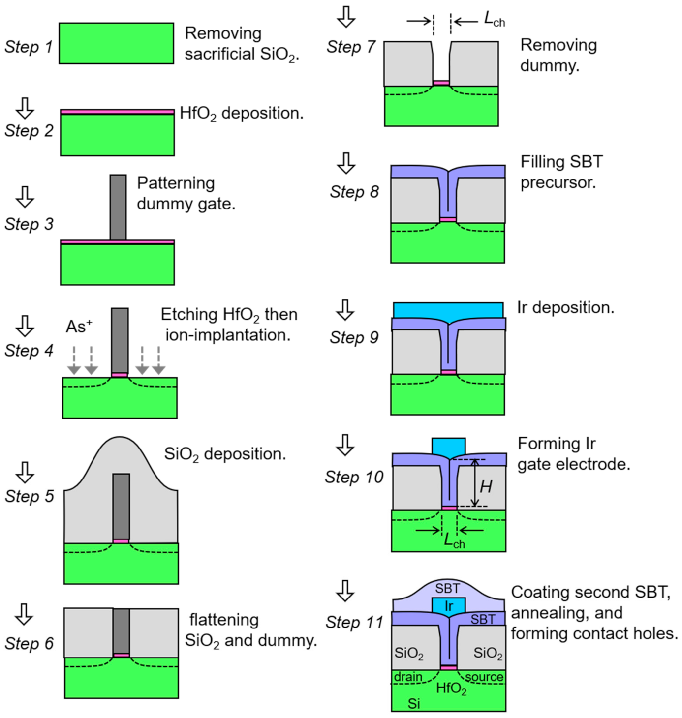
The fabrication process (schematic drawings shown in Figure 1) in this work is as follows:
- Step 1: Si substrate preparation.A p-type Si substrate patterned with FET active areas was prepared. Local-oxidation-of-silicon (LOCOS) process was used in the patterning for device isolation. The LOCOS patterns with various channel widths (W) were designed in a sample chip. Areas for source-, drain- and substrate-contact holes on the Si were heavily ion-doped. Sacrificial SiO2 on Si was removed with buffered hydrogen fluoride.
- Step 2: Insulator deposition.
- Step 3: Lithography.Electron-beam (EB) lithography was performed by spin-coating an organic resist, exposing 130 kV EB, and developing. Resist patterns 550 nm tall were left on the HfO2/Si. They were later used as ion-implantation mask in Step 4 and as dummy gates in Step 7.
- Step 4: Ion implantation.HfO2 uncovered with resist was etched out by inductively-coupled-plasma reactive-ion etching (ICP-RIE). On the exposed Si, As+ ions were implanted for source and drain. The energy and dose conditions were 4 keV and 5.0 × 10¹²/cm2.
- Step 5: SiO2 deposition.An 830 nm thick SiO2 was deposited to cover the resist patterns on the substrate by 300 W rf sputtering in 0.1 Pa Ar.
- Step 6: Flattening SiO2.The SiO2 was etched back and flattened by ICP-RIE with 1.0 Pa Ar-CF4 mixed gas until tops of the resists or dummy gates were exposed.
- Step 7: Leaving grooves on gates.The dummy-gate substances were selectively removed by O2 plasma ashing. There remained grooves in a 410 nm tall SiO2 isolation. The grooves were located on the HfO2 with self-aligned source and drain regions prepared in Step 4. The whole chip was rapidly annealed at 800 °C in ambient N2.
- Step 8: Ferroelectric deposition.SBT precursor film was deposited to fill up the grooves by a metal-organic-chemical-vapor deposition (MOCVD) system (WACOM R&D, Nihonbashi, Tokyo, Japan). Sources of Bi(C5H11O2)3, Sr[Ta(OC2H5)5(OC2H4OCH3)]2 and Ta(OCH2CH3)5 (Tri Chemical Laboratories Inc., Uenohara, Yamanashi, Japan) were used [6]. As-deposited precursor-film thickness was estimated as 80 nm on a flat place of the substrate.
- Step 9: Metal deposition.Ir was deposited by rf sputtering on the SBT precursor layer. Resist mask was patterned for gate electrodes by EB lithography.
- Step 10: Forming gate electrodes.Ir uncovered with resist was etched out by Ar+ ion milling. Then, the resist mask was removed by O2 plasma ashing.
- Step 11: FeFET completed.SBT precursor was deposited again by MOCVD to cover the substrate [6]. The whole substrate was annealed for crystallization of the SBT to show ferroelectricity. The annealing condition was at 780 °C in an O2-N2 mixed gas we investigated before [8]. Finally, contact holes for gate, source, drain and substrate were formed by ultraviolet g-line lithography and Ar+ ion milling.
2.2. Reason for Using SBT in FeFET
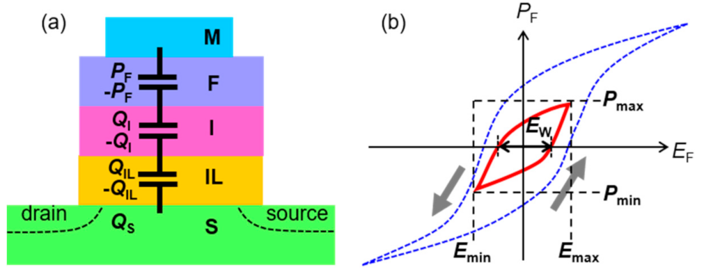
The gate stack of MFIS should be regarded as MFI(IL)S, as shown in in Figure 2a, where F, I, IL, S are connected in series. The IL is an interfacial layer between I and S which is formed during the ferroelectric crystallization annealing process of FeFETs [8,39,55,56,57]. The main component of IL is silicon dioxide with an electric permittivity (εIL) of εIL = 3.9. In the MFI(IL)S, |PF| ≈ ε0·εI·|EI| = ε0·εIL·|EIL| = |QS| is satisfied in any time. The PF is ferroelectric polarization. EI and EIL are electric fields in the I and the IL. The QS is charge area density in the semiconductor surface. The εI is a relative permittivity of the I. The ε0 is the vacuum dielectric constant of ε0 = 8.85 × 10⁻¹² F/m. For a simplified explanation, we assumed a virtual equivalent circuit of series capacitance as drawn in Figure 2a which is expressed by |PF| ≈ |QI| = |QIL| = |QS| with virtual charges QI and QIL on I and IL, respectively. In MFI(IL)S, the IL suffers from a stress of field |EIL| ≈ |PF|/(ε0·εIL) = 8.7 MV/cm even at a small |PF| = 3 μC/cm2. For example, real IL thickness is 2.6 nm [8] or about 1 nm [55,56,57]. Electric-field-assisted tunnel current through such a thin SiO2 [58,59] brings charge injection into the gate stack from S across IL. In erase-and-program operations, a large EIL derived from a large PF swing induces significant trapped-charge accumulation which accelerates endurance degradations [2,52]. According to our experience [43,52,60], |PF| should normally be less than 2.5 μC/cm2 all the time and should not exceed 2.0 μC/cm2 for further high-endurance requirements of the FeFET.
Ferroelectric materials show PF versus EF hysteresis loops as illustrated in Figure 2b. The EF is the electric field across the F. We defined Emax as the positive maximum EF and Pmax as the PF at EF = Emax. Similarly, Emin and Pmin are the negative minimum EF and the PF at EF = Emin. The loop is called “major” loop when the Emax and |Emin| are strong enough to force PF saturated, whereas it is called “minor” loop when PF is unsaturated by moderate EF swing. In SBT-FeFETs, restrictions of Pmax ≤ 2.5 μC/cm2 corresponding to the minor loops are used during all operations as we emphasized in early works [39,43,52,60].
Regarding a ferroelectric hidden in MFI(IL)S, an exact symmetric swing maximum, i.e., Pmax = |Pmin| or Emax = |Emin|, is difficult because |QS| versus ΦS is very asymmetric [61,62]. The QS is the charge area density of the semiconductor surface and ΦS is the surface potential. Presence of the flat-band voltage Vfb makes the symmetric swing further difficult. However, to simplify the physical explanation, Pmax = |Pmin| and Emax = |Emin| are assumed as shown in Figure 2b with Vfb = 0V. In every PF-EF loop, the EF width at PF = 0 is defined as Ew being related with a voltage memory window (Vw) by an approximate expression Ew = 2Ec = Vw/dF, where the Ec is a coercive field and dF is ferroelectric thickness. According to a method we proposed before [43], an important characteristic Emax of the ferroelectric can be evaluated which has not been measurable by direct probing on a FeFET. If Pmax is provided, a gate voltage Vg to achieve a target memory window Vw = Ew·dF can be estimated as a sum of Emax·dF, EI·dI, EIL·dIL and ΦS at QS = Pmax. An exact discussion can be found in the paper [43].
For instance, Pt/SBT/HAO/Si FeFETs showed Ew = 18 kV/cm at Pmax = 2.0 μC/cm2 and Emax = 25 kV/cm [43]. By adopting an advanced process [8], Ir/CSBT/HfO2/Si FeFETs had the best improved values of Ew = 65 kV/cm at Pmax = 2.0 μC/cm2 and Emax = 140 kV/cm [3,43]. A good reason for using (C)SBT in Si-based FeFETs is the (C)SBT ferroelectric nature of a convenient minor PF-EF loop [14,17,20] which has Ew available and is controllable in a restricted PF range of Pmax ≤ 2 μC/cm2 with Emax ≤ 140 kV/cm.
There are some other ferroelectric materials also intensively studied for applications in Si-based MFIS FeFETs. Regarding Pb5Ge3O11 (PGO), attempts to develop replacement-gate-type Pt/PGO/ZrO2/Si FeFETs were reported [63] but the erase-program-test results of the FeFETs were not found although the ferroelectric itself showed a good potential Pmax-Emax and Ew − Emax judging from hysteresis loops of the PGO metal/ferroelectric/metal capacitors [64]. Regarding another candidate, the ferroelectric HfO2 family [55,56,57,65,66,67,68,69,70], the intrinsic material nature may not be suitable for applying to Si-based FeFETs. Informative minor hysteresis loops were reported on Y-doped HfO2 in which Ew seemed nearly equal to 0 V/cm at Pmax = 2.0 μC/cm2, although it was as large as about 1 MV/cm at Pmax = 10 μC/cm2 [66]. Operation of the FeFETs under the restriction of Pmax ≤ 2 μC/cm2 may be difficult. Some reports suggested that HfO2-FeFETs cannot help using a large Pmax (>>2 μC/cm2) [52,55]. The large Pmax may induce significant charge injection into the gate stack. As far as we know, fair works on HfO2-FeFETs have not cleared 108 cycles endurance in spite of using sophisticated production facilities [56,67,68,69,70].
3. Results and Discussion
3.1. Device Dimensions
A cross-sectional scanning-electron-microscope photograph of an Ir/SBT/HfO2/Si FeFET fabricated by the new proposed process is shown in Figure 3a. Figure 3b shows the same picture added with support lines to clarify the material boundaries. The schematic drawing of the FeFET was assigned with four terminals of gate, drain, source and substrate (Figure 3c). The gate-channel length (Lch) was Lch = 85 nm. The gate-channel width was W = 100 μm depending on the initial LOCOS pattern designed in Step 1 in Section 2.1. The metal-gate length Lm was 150 nm which could be shorter but was not the focus in this work. The SBT precursor film thickness was about 80 nm measured on a flat place. By filling gate grooves with SBT precursor (Step 8 in Section 2.1.), the effective SBT height (H) was finally about 450 nm which was a distance between Ir and HfO2. Area scalability of the new FeFET was equivalent to that of the dummy gates which are organic resist patterns made by lithography. From the viewpoint of Si transistor technology, Lch = 10 nm is expected to be the critical limit [71]. A significant Curie-temperature decrease in SBT started when particle were sizes of around 20 nm [25]. Thus, the prospective shortest limit of Lch by our proposed FeFET process may be around 20 nm.
3.2. Electrical Characterizations
In this study, memory windows, endurance and retention of FeFETs were investigated at room temperature. A semiconductor parameter analyzer (4156C, Keysight Technologies, Santa Rosa, CA, USA) was used for measuring static drain current versus gate voltage (Id–Vg) curves of the FeFETs. A pulse generator (81110A, Keysight Technologies, Santa Rosa, CA, USA) was used to apply Vg pulses. The instruments were computer-controlled using programs written by the language of LabVIEW (ver. 10, National Instruments, Austin, TX, USA).
3.2.1. Memory Windows
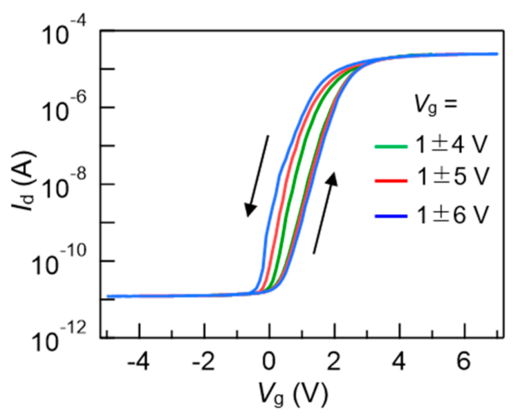
As an elementary test of the FeFETs, Id–Vg hysteresis loops were investigated (Figure 4). The Id was measured by Vg increments and decrements with 0.1 V steps. The Vg sweeping ranges were Vg = 1 ± 4 V, 1 ± 5 V and 1 ± 6 V. Drain voltage (Vd), source voltage (Vs) and substrate voltage (Vsub) were fixed to Vd = 0.1 V and Vs = Vsub = 0 V during the measurements. The Id–Vg showed hysteresis loops drawn in counter-clockwise directions because the FeFET was an n-channel-type one. In an Id–Vg curve, threshold voltage (Vth) was defined as a Vg value at Id/W = 1 × 10⁻⁷ A/cm. Two Vth values were extracted from the left- and right-side curves in an Id–Vg hysteresis loop. A memory window was defined as the Vth difference. In this work, we call this a static memory window (Vw) because Vg sweep by 4156C is slow. The static Vw was, for instance, 1.0 V by sweeping Vg from −5 to 7 V then back to −5 V, or at Vg = 1 ± 6 V as expressed in Figure 4. During the measurement of a wide-range Id from 10−12 to 10−4 A as indicated in Figure 4, Vg sweep speed depends on the current range. Therefore, an Id–Vg hysteresis curve only gives reference information that is not suitable for accurate discussion.
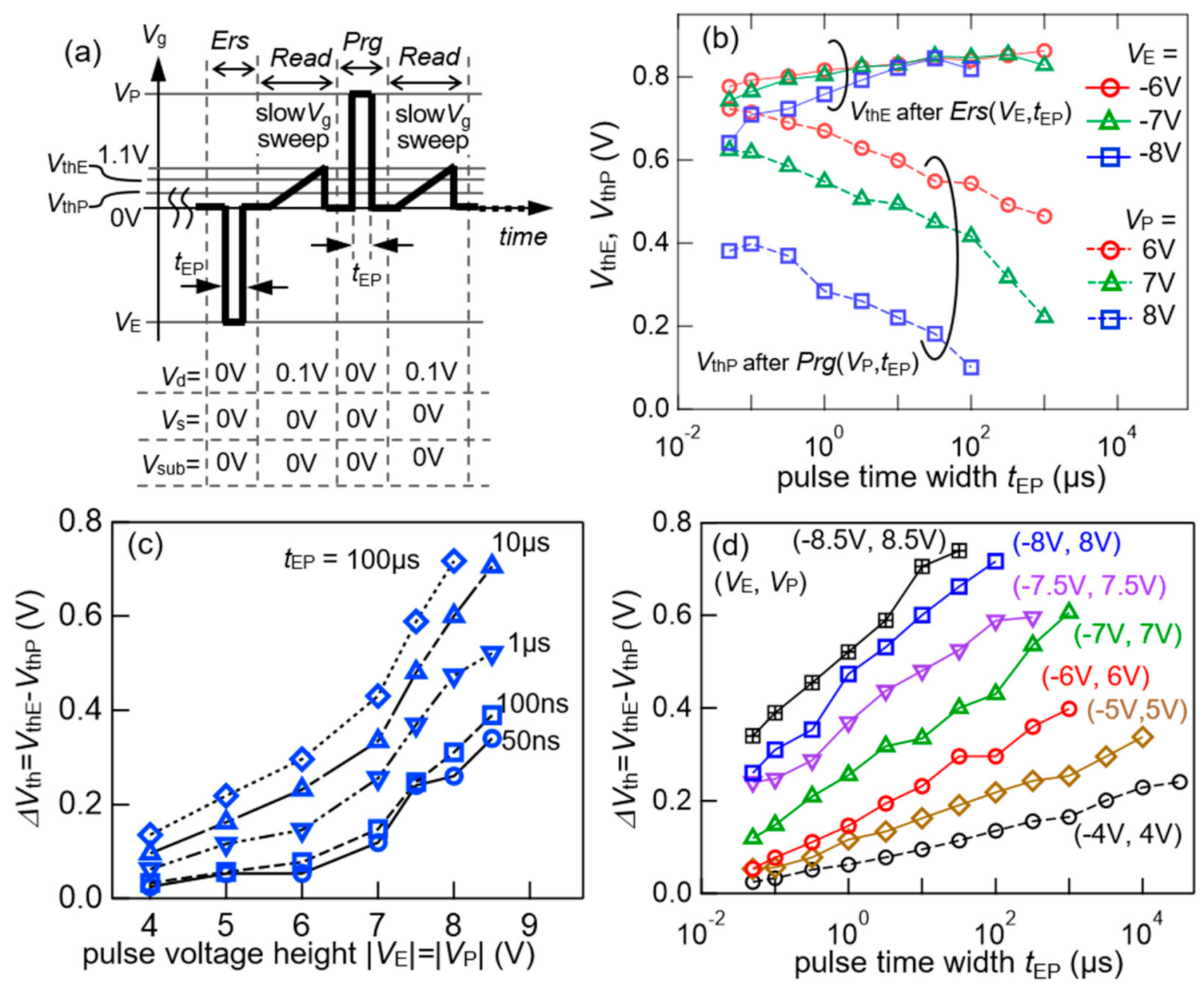
For an accurate understanding, the FeFET performance, a pulsed Vg with a controlled time width, was applied to the FeFETs for the erase (Ers) or program (Prg) operation. The Vg pulse heights with the time widths were (VE, tE) for Ers, and (VP, tP) for Prg, respectively. For the n-channel-type FeFET, the VE was negative (VE < 0 V) and VP was positive (VP > 0 V) [9]. The pulse time widths tE and tP were the same with each other in this work (tE = tP = tEP). After, Ers and Prg, Id–Vg curves were individually measured with a small common Vg range for Read. Two Vth values were defined in the Id–Vg curves as the Vg at Id/W = 1 × 10⁻⁷ A/cm. They were expressed as VthE after Ers and VthP after Prg. The VthE was larger than the VthP [9]. The Vth difference of ΔVth = VthE − VthP was defined as a memory window obtained by read operation after erase-and-program pulse applications. The memory window ΔVth is normally smaller than the above-mentioned static Vw, because slow switching components in a ferroelectric do not respond to short pulses [27,72,73]. The VthE and VthP were investigated by repeating a series of operations: Ers, Read, Prg, Read, in this order (Figure 5a). In Ers, a pulsed Vg of (VE, tEP) was applied with keeping Vd = Vs = Vsub = 0 V. In Read after Ers, a VthE was extracted from an Id-Vg curve drawn by narrow-range varying Vg from 0 to 1.1 V at Vd = 0.1 V and Vs = Vsub = 0 V. In Prg, a pulsed Vg of (VP, tEP) was applied, keeping Vd = Vs = Vsub = 0 V. In Read after Prg, a VthP was extracted from an Id–Vg curve drawn under exactly the same conditions as those in Read after Ers.
Figure 5b shows VthE and VthP by Read after Ers and Prg for three sets of (VE, tEP) and (VP, tEP) of |VE| = VP = 6, 7 and 8 V. Every marker corresponds to the measured VthE and VthP. Memory windows, ΔVth = VthE-VthP, as a function of pulse height |VE| = |VP| (Figure 5c) and width tEP (Figure 5d) can be seen in Figure 5b, where the VthE and VthP results (not shown in Figure 5b) of other VP (=|VE|) conditions were also used. Short Vg pulses of tEP = 50 ns were available for Ers and Prg of the FeFET. Memory windows of ΔVth > 0.7 V were obtained using 8 and 8.5 V pulses.
Figure 5c,d show a clear monotonic ΔVth increases when raising either the pulse height or width. Good analog VthE and VthP controllability was suggested by smooth and linear ΔVth growths with raising log(tEP) as shown in Figure 5d. The similar tendencies of ΔVth and tEP have already been reported in our previous works [3,5,7,9,52]. In the prior FeFETs, poly-crystalized ferroelectrics were visualized by electron backscatter diffraction (EBSD) [44]. The EBSD indicated that the (C)SBT consisted of multi-grains with various crystal orientations in the FeFETs. The poly-crystalized ferroelectrics may bring the analog VthE and VthP controllability to the FeFETs. In the present FeFET, there must be numerous grains in channel-width direction with W = 100 μm whereas a single grain or a few were expected in channel-length with Lch = 85 nm which was smaller than average diameters of SBT grains freely grown in-plane [44].
In a preferable geometry of the replacement-gate FeFET in the future, only the channel area Lch × W will be intensively scaled down with remaining the height H. The H is decided by the gate-groove depth in Step 7 in Section 2.1 and Figure 1. The ΔVth in this report was not yet at its best ability considering the ferroelectric height H = 450 nm. In the vertical direction of FeFET, a gate stack by filling SBT should be essentially the same as a large Lch conventional one by etching SBT. Therefore, potential ΔVth will become the same as that of conventional FeFETs by improving the details in the fabrication process in Section 2.1. An immediate target for the present FeFET will be realizing ΔVth = 0.7 V by Ers of (−6V, 10 μs) and Prg of (6V, 10 μs) for H = 190 nm as demonstrated before using Pt/CSBT/HfO2/Si FeFETs [7].
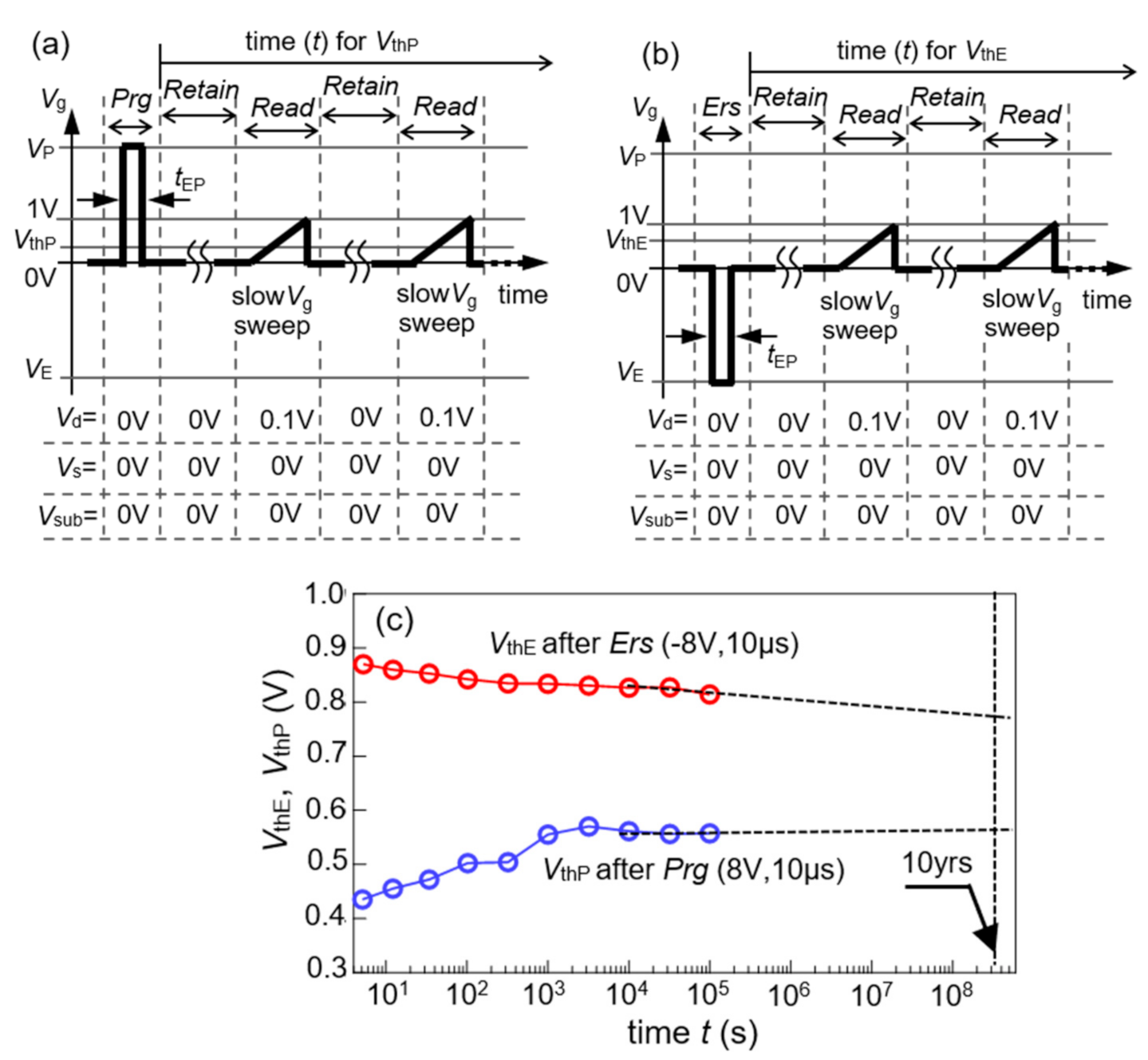
3.2.2. Retention
Retention of a FeFET was measured by the procedures as shown in Figure 6a,b. After program (Prg), Retain and Read were repeated during the scheduled time. In Prg, a Vg pulse of (VP, tEP) was applied with Vd = Vs = Vsub = 0 V. In Retain, all the terminals were kept at zero as Vg = Vd = Vs = Vsub = 0 V. In Read at a certain time t, an Id–Vg curve was drawn by varying Vg in a narrow range from 0 to 1.0 V at Vd = 0.1 V and Vs = Vsub = 0 V. A VthP was extracted from the Id–Vg and plotted with a marker at t as shown in Figure 6c. After completing the VthP-t, VthE-t started to be measured. In erase (Ers), a Vg pulse of (VE, tEP) was applied with Vd = Vs = Vsub = 0 V. After Ers, Retain and Read were repeated during the scheduled time. The Retain and Read conditions for VthE-t were the same as those for VthP-t. In the Read at a certain time t, an extracted VthE was plotted with a marker at t as shown in Figure 6c. In this work, VP = 8 V, VE = −8 V and tEP = 10 μs. The retention was measured for 105 s in each of VthP–t and VthE–t. At t = 105 s, they were still distinguishable with a difference ΔVth = 0.26 V. When t > 103 s, as shown in Figure 6c, the gradient of the VthP-log(t) and VthE–log(t) curves appeared to be nearly zero. A possible ten-year retention was suggested by extrapolation lines drawn on the last three markers in each branch. The present Lch = 85 nm FeFET showed a good retention to the same extent as those of the conventional (C)SBT FeFETs [1,2,3,4,5,6,7,8,9,11,12,37,38,39,40,42,45,46,52].
3.2.3. Endurance
Endurance of a FeFET was measured by the procedure shown in Figure 7a. After imposing endurance cycles on FeFETs, pairs of VthE and VthP were obtained. The endurance cycles consisted of periodic bipolar Vg pulses for an alternate Ers of (VE, tEP) and Prg of (VP, tEP) with Vd = Vs = Vsub = 0 V. The endurance-cycle application was interrupted at certain scheduled cycle numbers (N). After the N cycle application, VthE and VthP were read as follows: a series operation of Ers, Read, Prg, and Read, in this order was performed. In Ers, a single Vg pulse of (VE, tEP) was applied with Vd = Vs = Vsub = 0 V. In Read after Ers, an Id-Vg was measured by varying Vg in a narrow range from 0 to 1.5 V at Vd = 0.1 V and Vs = Vsub = 0 V. A VthE was extracted from the Id–Vg and plotted with a marker at N as shown in Figure 7b. In Prg, a single Vg pulse of (VP, tEP) was applied with Vd = Vs = Vsub = 0 V. In Read after Prg, an Id–Vg was measured under the same conditions with Read after Ers. The obtained VthP was plotted with a marker at N as shown in Figure 7b.
As shown in Figure 7b, the Ers of (−7.5 V, 10 μs) and Prg of (7.5 V, 10 μs) were first applied for an endurance up to N = 108 cycles. Next, a stronger input of (−8 V, 10 μs) and (8 V, 10 μs) was applied to the same FeFET up to N = 109 cycles. No significant sifts of VthE and VthP were observed throughout the measurements. By taking the minimum of the VthE and the maximum of the VthP in the endurance test, ΔVth = 0.40 V for |VE| = VP = 7.5 V and ΔVth = 0.57 V for |VE| = VP = 8 V were obtained. These were margins for distinguishing VthE from VthP as indicated in Figure 7b. In spite of using the rather complicated dummy-gate process, the Lch = 85 nm FeFET fabricated showed high endurance up to 108~109 cycles. This is the same as the endurance level that (C)SBT-FeFETs inherently have [1,2,3,4,5,6,7,8,9,10,11,12].
4. Summary
A new fabrication process of a FeFET was proposed and demonstrated. Dummy-gate patterns with self-aligned sources and drains were prepared on a Si substrate. HfO2 with a thickness of 5 nm was inserted in advance between the dummy-gate substance and the Si substrate. The dummy substance was selectively removed to form a self-aligned groove on the gate. A thin SBT precursor film was deposited to fill up the groove. After forming the Ir gate electrode on the SBT, the whole gate stack was annealed for the SBT crystallization. The finished FeFET of Ir/SBT/HfO2/Si had a channel length Lch = 85 nm. The FeFET exhibited a 109 cycle-high endurance and long stable retentions measured for 105 s. By adopting the replacement-gate process, area-scalable SBT-FeFETs with the high endurance and long retention were successfully produced.
Author Contributions
Conceptualization followed by numerous improvements with respect to the device structure and processing, M.T.; the anneal and MOCVD processes, S.S.; SEM observation, M.T.; creation of PC-controlled measurement programs, S.S.; electrical measurement of the devices, S.S.; data analysis and discussion, S.S. and M.T.; writing—original draft preparation, M.T.; writing—review and editing, M.T. and S.S. All authors have read and agreed to the published version of the manuscript.
Funding
This research received no external funding.
Institutional Review Board Statement
Not applicable.
Informed Consent Statement
Not applicable.
Data Availability Statement
Not applicable.
Acknowledgments
This work was partially supported by WACOM R&D Corporation. We used the EB lithography system in the NPF of AIST, supported by MEXT, Japan.
Conflicts of Interest
The authors declare no conflict of interest.
References
- Sakai, S.; Ilangovan, R. Metal-ferroelectric-insulator-semiconductor memory FET with long retention and high endurance. IEEE Electron Device Lett. 2004, 25, 369–371. [Google Scholar] [CrossRef]
- Yan, K.; Takahashi, M.; Sakai, S. Electrical properties of ferroelectric-gate FETs with SrBi2Ta2O9 formed using MOCVD technique. Appl. Phys. A Mater. Sci. Process. 2012, 108, 835–842. [Google Scholar] [CrossRef]
- Sakai, S.; Zhang, W.; Takahashi, M. Dynamic analog characteristics of 109 cycle-endurance low-voltage nonvolatile ferroelectric-gate memory transistors. In Proceedings of the 2017 IEEE 9th International Memory Workshop, Monterey, CA, USA, 14–17 May 2017; pp. 95–98. [Google Scholar] [CrossRef]
- Hai, L.V.; Takahashi, M.; Sakai, S. Fabrication and characterization of sub-0.6-μm ferroelectric-gate field-effect transistors. Semicond. Sci. Technol. 2010, 25, 115013. [Google Scholar] [CrossRef]
- Zhang, W.; Takahashi, M.; Sakai, S. Electrical properties of CaxSr1-xBi2Ta2O9 ferroelectric-gate field-effect transistors. Semicond. Sci. Technol. 2013, 28, 085003. [Google Scholar] [CrossRef]
- Hai, L.V.; Takahashi, M.; Zhang, W.; Sakai, S. Novel process for widening memory window of sub-200nm ferroelectric-gate field-effect transistor by ferroelectric coating the gate-stack sidewall. Semicond. Sci. Technol. 2015, 30, 015024. [Google Scholar] [CrossRef]
- Hai, L.V.; Takahashi, M.; Zhang, W.; Sakai, S. 100-nm-size ferroelectric-gate field-effect transistor with 108-cycle endurance. Jpn. J. Appl. Phys. 2015, 54, 088004. [Google Scholar] [CrossRef]
- Zhang, W.; Takahashi, M.; Sasaki, Y.; Kusuhara, M.; Sakai, S. 3.3 V write-voltage Ir/Ca0.2Sr0.8Bi2Ta2O9/HfO2/Si ferroelectric-gate field-effect transistors with 109 endurance and good retention. Jpn. J. Appl. Phys. 2017, 56, 04CE04. [Google Scholar] [CrossRef]
- Sakai, S.; Takahashi, M.; Takeuchi, K.; Li, Q.-H.; Horiuchi, T.; Wang, S.; Yun, K.-Y.; Takamiya, M.; Sakurai, T. Highly scalable Fe(ferroelectric)-NAND cell with MFIS(metal-ferroelectric-insulator-semiconductor) structure for sub-10nm tera-bit capacity NAND flash memories. In Proceedings of the 2008 Joint Non-Volatile Semiconductor Memory Workshop and International Conference on Memory Technology and Design, Opio, France, 18–22 May 2008; pp. 103–105. [Google Scholar] [CrossRef]
- Zhang, X.; Miyaji, K.; Takahashi, M.; Takeuchi, K.; Sakai, S. 0.5V bit-line-voltage self-boost-programming in ferroelectric-NAND flash memory. In Proceedings of the 2011 3rd IEEE International Memory Workshop, Monterey, CA, USA, 22–25 May 2011; pp. 155–158. [Google Scholar] [CrossRef]
- Zhang, X.; Takahashi, M.; Takeuchi, K.; Sakai, S. 64 kbit ferroelectric-gate-transistor-integrated NAND flash memory with 7.5 V program and long data retention. Jpn. J. Appl. Phys. 2012, 51, 04DD01. [Google Scholar] [CrossRef]
- Takahashi, M.; Zhang, W.; Sakai, S. High-endurance ferroelectric NOR flash memory using (Ca,Sr)Bi2Ta2O9 FeFETs. In Proceedings of the 2018 IEEE 10th International Memory Workshop, Kyoto, Japan, 13–16 May 2018; pp. 58–61. [Google Scholar] [CrossRef]
- De Araujo, C.A.P.; Cuchiaro, J.D.; McMillan, L.D.; Scott, M.C.; Scott, J.F. Fatigue-free ferroelectric capacitors with platinum electrodes. Nature 1995, 374, 627–629. [Google Scholar] [CrossRef]
- Noguchi, T.; Hase, T.; Miyasaka, Y. Analysis of the dependence of ferroelectric properties of strontium bismuth tantalate (SBT) thin film on the composition and process temperature. Jpn. J. Appl. Phys. 1996, 35, 4900–4904. [Google Scholar] [CrossRef]
- Lettieri, J.; Jia, Y.; Urbanik, M.; Weber, C.I.; Maria, J.-P.; Schlom, D.G.; Li, H.; Ramesh, R.; Uecker, R.; Reiche, P. Epitaxial growth of (001)-oriented and (110)-oriented SrBi2Ta2O9 thin films. Appl. Phys. Lett. 1995, 66, 221–223. [Google Scholar] [CrossRef]
- Ishikawa, K.; Funakubo, H. Electrical properties of (001)- and (116)-oriented epitaxial SrBi2Ta2O9 thin films prepared by metalorganic chemical vapor deposition. Appl. Phys. Lett. 1999, 75, 1970–1972. [Google Scholar] [CrossRef]
- Ishikawa, K.; Funakubo, H.; Saito, K.; Suzuki, T.; Nishi, Y.; Fujimoto, M. Crystal structure and electrical properties of epitaxial SrBi2Ta2O9 films. J. Appl. Phys. 2000, 87, 8018–8023. [Google Scholar] [CrossRef]
- Lee, H.N.; Visinoiu, A.; Senz, S.; Harnagea, C.; Pignolet, A.; Hesse, D.; Gösele, U. Structural and electrical anisotropy of (001)-, (116)-, and (103)-oriented epitaxial SrBi2Ta2O9 thin films on SrTiO3 substrates grown by pulsed laser deposition. J. Appl. Phys. 2000, 88, 6658–6664. [Google Scholar] [CrossRef]
- Amanuma, K.; Hase, T.; Miyasaka, Y. Preparation and ferroelectric properties of SrBi2Ta2O9 thin films. Appl. Phys. Lett. 1995, 66, 221–223. [Google Scholar] [CrossRef]
- Atsuki, T.; Soyama, N.; Yonezawa, T.; Ogi, K. Preparation of Bi-based ferroelectric thin films by Sol-Gel method. Jpn. J. Appl. Phys. 1995, 34, 5096–5099. [Google Scholar] [CrossRef]
- Robertson, J.; Chen, C.W.; Warren, W.L.; Gutleben, C.D. Electronic structure of the ferroelectric layered perovskite SrBi2Ta2O9. Appl. Phys. Lett. 1996, 69, 1704–1706. [Google Scholar] [CrossRef]
- Harnagea, C.; Pignolet, A.; Alexe, M.; Hesse, D.; Gösele, U. Quantitative ferroelectric characterization of single submicron grains in Bi-layered perovskite thin films. Appl. Phys. A 2000, 70, 261–267. [Google Scholar] [CrossRef]
- Kalinin, S.V.; Gruverman, A.; Bonnell, D.A. Quantitative analysis of nanoscale switching in SrBi2Ta2O9 thin films by piezoresponse force microscopy. Appl. Phys. Lett. 2004, 85, 795. [Google Scholar] [CrossRef]
- Amorín, H.; Shvartsman, V.V.; Kholkin, A.L.; Costa, M.E.V. Ferroelectric and dielectric anisotropy in high-quality SrBi2Ta2O9 single crystals. Appl. Phys. Lett. 2004, 85, 5667. [Google Scholar] [CrossRef]
- Yu, T.; Shen, Z.X.; Toh, W.S.; Xue, J.M.; Wang, J. Size effect on the ferroelectric phase transition in SrBi2Ta2O9 nanoparticles. J. Appl. Phys. 2003, 94, 618–620. [Google Scholar] [CrossRef]
- Gruverman, A. Scaling effect on statistical behavior of switching parameters of ferroelectric capacitors. Appl. Phys. Lett. 1999, 75, 1452–1454. [Google Scholar] [CrossRef]
- Tamura, T.; Arimoto, Y.; Ishiwara, H. A New Circuit Simulation Model of Ferroelectric Capacitors. Jpn. J. Appl. Phys. 2002, 41, 2654–2657. [Google Scholar] [CrossRef]
- Pan, B.; Yu, H.; Wu, D.; Zhou, X.H.; Liu, J.-M. Dynamic response and hysteresis dispersion scaling of ferroelectric SrBi2Ta2O9 thin films. Appl. Phys. Lett. 2003, 83, 1406–1408. [Google Scholar] [CrossRef]
- Lee, W.-J.; Cho, C.-R.; Kim, S.-H.; You, I.-K.; Kim, B.W.; Yu, B.-G.; Shin, C.H.; Lee, H.C. Etching Behavior and Damage Recovery of SrBi2Ta2O9 Thin Films. Jpn. J. Appl. Phys. 1999, 38, L1428–L1431. [Google Scholar] [CrossRef]
- Asami, K.; Koiwa, I.; Yamanobe, T. Effects of Ion Etching and Annealing in O2 Atmosphere Following Ion Etching on Properties and Chemistry of Sr0.9Bi2.1Ta2O9+α Thin Films. Jpn. J. Appl. Phys. 1999, 38, 5423–5427. [Google Scholar] [CrossRef]
- Stafford, L.; Margot, J.; Delprat, S.; Chaker, M.; Pearton, S.J. Influence of redeposition on the plasma etching dynamics. J. Appl. Phys. 2007, 101, 083303. [Google Scholar] [CrossRef]
- Efremov, A.M.; Kim, D.-P.; Kim, C.-I. Investigation of thin films etching mechanisms in plasma. J. Vsc. Sci. Technol. A 2003, 21, 1017–1023. [Google Scholar] [CrossRef]
- Shimakawa, Y.; Kubo, Y.; Nakagawa, Y.; Goto, S.; Kamiyama, T.; Asano, H.; Izumi, F. Crystal structure and ferroelectric properties of ABi2Ta2O9 (A = Ca, Sr, and Ba). Phys. Rev. B 2000, 61, 6559–6564. [Google Scholar] [CrossRef]
- Noguchi, Y.; Shimizu, H.; Miyayama, M.; Oikawa, K.; Kamiyama, T. Ferroelectric properties and structure distortion in A-site-modified SrBi2Ta2O9. Jpn. J. Appl. Phys. 2001, 40, 5812–5815. [Google Scholar] [CrossRef]
- Das, R.R.; Bhattacharya, P.; Pe´rez, W.; Katiyar, R.S. Ferroelectric properties of laser-ablated Sr1-xAxBi2Ta2O9 thin films (where A = Ba, Ca). Appl. Phys. Lett. 2002, 80, 637–639. [Google Scholar] [CrossRef]
- Das, R.R.; Bhattacharya, P.; Pe´rez, W.; Katiyar, R.S. Influence of Ca on structural and ferroelectric properties of laser ablated SrBi2Ta2O9 thin films. Jpn. J. Appl. Phys. 2003, 42, 162–165. [Google Scholar] [CrossRef]
- Development of the 1T FeRAM: Towards the Realization of the Ultra-Gbit Next-Generation Semiconductor Memory. AIST Research Results Archive, 24 October 2002. Available online: https://www.aist.go.jp/aist_e/list/latest_research/2002/20021024/20021024.html (accessed on 14 December 2020).
- Sakai, S.; Takahashi, M.; Ilangovan, R. Long-retention ferroelectric-gate FET with a (HfO2)x(Al2O3)1-x buffer-insulating layer for 1T FeRAM. In Proceedings of the 2004 IEDM Technical Digest. IEEE International Electron Devices Meeting, San Francisco, CA, USA, 13–15 December 2004; pp. 915–918. [Google Scholar] [CrossRef]
- Sakai, S.; Ilangovan, R.; Takahashi, M. Pt/SrBi2Ta2O9/Hf-Al-O/Si field-effect-transistor with long retention using unsaturated ferroelectric polarization switching. Jpn. J. Appl. Phys. 2004, 43, 7876–7878. [Google Scholar] [CrossRef]
- Li, Q.H.; Sakai, S. Characterization of Pt/SrBi2Ta2O9/Hf-Al-O/Si field-effect transistors at elevated temperatures. Appl. Phys. Lett. 2006, 89, 222910. [Google Scholar] [CrossRef]
- Li, Q.H.; Takahashi, M.; Horiuchi, T.; Wang, S.Y.; Sakai, S. Threshold-voltage distribution of Pt/SrBi2Ta2O9/Hf-Al-O/Si MFIS FETs. Semicond. Sci. Technol. 2008, 23, 045011. [Google Scholar] [CrossRef]
- Li, Q.H.; Horiuchi, T.; Wang, S.Y.; Takahashi, M.; Sakai, S. Threshold voltage adjustment of ferroelectric-gate field effect transistors by ion implantation. Semicond. Sci. Technol. 2009, 24, 025012. [Google Scholar] [CrossRef]
- Sakai, S.; Zhang, W.; Takahashi, M. Method for disclosing invisible physical properties in metal-ferroelectric-insulator-semiconductor gate stacks. J. Phys. D Appl. Phys. 2017, 50, 165107. [Google Scholar] [CrossRef]
- Zhang, W.; Takahashi, M.; Sakai, S. Investigation of ferroelectric grain sizes and orientations in Pt/CaxSr1–xBi2Ta2O9/Hf–Al–O/Si high performance ferroelectric-gate field-effect-transistors. Materials 2019, 12, 399. [Google Scholar] [CrossRef] [Green Version]
- Takahashi, M.; Sakai, S. Self-aligned-gate metal/ferroelectric/insulator/semiconductor field-effect transistors with long memory retention. Jpn. J. Appl. Phys. 2005, 44, L800–L802. [Google Scholar] [CrossRef]
- Horiuchi, T.; Takahashi, M.; Li, Q.H.; Wang, S.Y.; Sakai, S. Lowered operation voltage in Pt/SBi2Ta2O9/HfO2/Si ferroelectric-gate field-effect transistors by oxynitriding Si. Semicond. Sci. Technol. 2010, 25, 055005. [Google Scholar] [CrossRef]
- Takahashi, M.; Horiuchi, T.; Li, Q.H.; Wang, S.Y.; Sakai, S. Basic operation of novel ferroelectric CMOS circuits. Electron. Lett. 2008, 44, 467–468. [Google Scholar] [CrossRef]
- Takahashi, M.; Wang, S.Y.; Horiuchi, T.; Sakai, S. FeCMOS logic inverter circuits with nonvolatile-memory function. IEICE Electron. Express 2009, 6, 831–836. [Google Scholar] [CrossRef] [Green Version]
- Wang, S.Y.; Takahashi, M.; Li, Q.H.; Takeuchi, K.; Sakai, S. Operational method of a ferroelectric (Fe)-NAND flash memory array. Semicond. Sci. Technol. 2009, 24, 105029. [Google Scholar] [CrossRef]
- Miyaji, K.; Noda, S.; Hatanaka, T.; Takahashi, M.; Sakai, S.; Takeuchi, K. A 1.0 V power supply, 9.5 GByte/sec write speed, Single-Cell Self-Boost program scheme for Ferroelectric NAND Flash SSD. In Proceedings of the 2010 IEEE International Memory Workshop, Seoul, South Korea, 16–19 May 2010; pp. 1–4. [Google Scholar] [CrossRef]
- Zhang, X.; Takahashi, M.; Sakai, S. FeFET logic circuits for operating a 64 kb FeNAND flash memory array. Integr. Ferroelectr. 2012, 132, 114–121. [Google Scholar] [CrossRef]
- Sakai, S.; Zhang, X.Z.; Hai, L.V.; Zhang, W.; Takahashi, M. Downsizing and memory array integration of Pt/SrBi2Ta2O9/Hf-Al-O/Si ferroelectric-gate field-effect transistors. In Proceedings of the 2012 12th Annual Non-Volatile Memory Technology Symposium, Singapore, 31 October–2 November 2012; pp. 55–59. [Google Scholar] [CrossRef]
- Sakai, S.; Takahashi, M.; Motohashi, K.; Yamaguchi, Y.; Yui, N.; Kobayashi, T. Large-area pulsed-laser deposition of dielectric and ferroelectric thin films. J. Vac. Sci. Technol. A 2007, 25, 903–907. [Google Scholar] [CrossRef]
- Sakai, S. Semiconductor-Ferroelectric Storage Devices and Processes for Producing The Same. U.S. Patent 7,226,795, 2007. [Google Scholar]
- Böscke, T.S.; Müller, J.; Bräuhaus, D.; Schröder, U.; Böttger, U. Ferroelectricity in hafnium oxide: CMOS compatible ferroelectric field effect transistors. In Proceedings of the 2011 IEDM Technical Digest. IEEE International Electron Devices Meeting, Washington, DC, USA, 5–7 December 2011; pp. 24.5.1–24.5.4. [Google Scholar] [CrossRef]
- Müller, J.; Yurchuk, E.; Schlösser, T.; Paul, J.; Hoffmann, R.; Müller, S.; Martin, D.; Slesazeck, S.; Polakowski, P.; Sundqvist, J.; et al. Ferroelectricity in HfO2 enables nonvolatile data storage in 28 nm HKMG. In Proceedings of the 2012 Symposium on VLSI Technology, Honolulu, HI, USA, 12–14 June 2012; pp. 25–26. [Google Scholar] [CrossRef]
- Ali, T.; Polakowski, P.; Riedel, S.; Büttner, T.; Kämpfe, T.; Rudolph, M.; Pätzold, B.; Seidel, K.; Löhr, D.; Hoffmann, R.; et al. Silicon doped hafnium oxide (HSO) and hafnium zirconium oxide (HZO) based FeFET: A material relation to device physics. Appl. Phys. Lett. 2018, 112, 222903. [Google Scholar] [CrossRef]
- Fukuda, M.; Mizubayashi, W.; Kohno, A.; Miyazaki, S.; Hirose, M. Analysis of Tunnel Current through Ultrathin Gate Oxides. Jpn. J. Appl. Phys. 1998, 37, L1534–L1536. [Google Scholar] [CrossRef]
- Shrenk, A.; Heiser, G. Modeling and simulation of tunneling through ultra-thin gate dielectrics. J. Appl. Phys. 1997, 81, 7900–7908. [Google Scholar] [CrossRef] [Green Version]
- Takahashi, M.; Sakai, S. 2.3.3 Requirements to the F Layer, Chap.2 Development of high-endurance and long-retention FeFETs of Pt/CaySr1−yBi2Ta2O9/(HfO2)x(Al2O3)1−x/Si gate stacks. In Ferroelectric-Gate Field Effect Transistor Memories, 2nd ed.; Park, B.-E., Ishiwara, H., Okuyama, M., Sakai, S., Yoon, S.-M., Eds.; Springer: Singapore, Singapore, 2020; pp. 35–37. [Google Scholar] [CrossRef]
- Kingston, R.; Neustadter, S.F. Calculation of the Space Charge, Electric Field, and Free Carrier Concentration at the Surface of a Semiconductor. J. Appl. Phys. 1955, 26, 718–720. [Google Scholar] [CrossRef]
- Sze, S.M. Chap.7, MIS Diode and Charge-Coupled Device. In Physics of Semiconductor Devices, 2nd ed.; John Wiley & Sons: New York, NY, USA, 1981; pp. 366–369. [Google Scholar]
- Zhang, F.; Hsu, S.T.; Ono, Y.; Ulrich, B.; Zhuang, W.; Ying, H.; Stecker, L.; Evans, D.R.; Maa, J. Fabrication and characterization of sub-micron metal-ferroelectric-insulator-semiconductor field effect transistors with Pt/Pb5Ge3O11/ZrO2/Si structure. Jpn. J. Appl. Phys. 2001, 40, L635–L637. [Google Scholar] [CrossRef]
- Li, T.; Hsu, S.T.; Ulrich, B.; Ying, H.; Stecker, L.; Evans, D.; Ono, Y.; Maa, J.; Lee, J.J. Fabrication and characterization of a Pb5Ge3O11 one-transistor-memory device. Appl. Phys. Lett. 2001, 79, 1661–1663. [Google Scholar] [CrossRef]
- Müller, J.; Böscke, T.S.; Schröder, U.; Mueller, S.; Bräuhaus, D.; Böttger, U.; Frey, L.; Mikolajick, T. Ferroelectricity in simple binary ZrO2 and HfO2. Nano Lett. 2012, 12, 4318–4323. [Google Scholar] [CrossRef]
- Shimizu, T.; Katayama, K.; Kiguchi, T.; Akama, A.; Konno, T.J.; Sakata, O.; Funakubo, H. The demonstration of significant ferroelectricity in epitaxial Y-doped HfO2 film. Sci. Rep. 2016, 6, 32931. [Google Scholar] [CrossRef] [PubMed] [Green Version]
- Yurchuk, E.; Müller, J.; Hoffmann, R.; Paul, J.; Martin, D.; Boschke, R.; Schlösser, T.; Müller, S.; Slesazeck, S.; Bentum, R.; et al. HfO2-Based Ferroelectric Field-Effect Transistors with 260 nm Channel Length and Long Data Retention. In Proceedings of the 2012 IEEE International Memory Workshop, Milan, Italy, 20–23 May 2012; pp. 1–4. [Google Scholar] [CrossRef]
- Trentzsch, M.; Flachowsky, S.; Richter, R.; Paul, J.; Reimer, B.; Utess, D.; Jansen, S.; Mulaosmanovic, H.; Müller, S.; Slesazeck, S.; et al. A 28nm HKMG super low power embedded NVM technology based on ferroelectric FETs. In Proceedings of the 2016 IEEE International Electron Devices Meeting, San Francisco, CA, USA, 3–7 December 2016; pp. 11.5.1–11.5.4. [Google Scholar] [CrossRef]
- Mulaosmanovic, H.; Breyer, E.T.; Mikolajick, T.; Slesazeck, S. Ferroelectric FETs with 20-nm-Thick HfO2 Layer for Large Memory Window and High Performance. IEEE Trans. Electron. Devices 2019, 66, 3828–3833. [Google Scholar] [CrossRef]
- Zhou, H.; Ocker, J.; Mennenga, M.; Noack, M.; Müller, S.; Trentzsch, M.; Dünkel, S.; Beyer, S.; Mikolajick, T. Endurance and targeted programming behavior of HfO2-FeFETs. In Proceedings of the 2020 IEEE International Memory Workshop, Dresden, Germany, 17–20 May 2020; pp. 1–4. [Google Scholar] [CrossRef]
- Wong, H.; Iwai, H. On the scaling issues and high-κ replacement of ultrathin gate dielectrics for nanoscale MOS transistors. Microelectron. Eng. 2006, 83, 1867–1904. [Google Scholar] [CrossRef]
- Tagantsev, A.K.; Stolichnov, I.; Setter, N.; Cross, J.S.; Tsukada, M. Non-Kolmogorov-Avrami switching kinetics in ferroelectric thin films. Phys. Rev. B 2002, 66, 214109. [Google Scholar] [CrossRef]
- Jo, J.Y.; Yang, S.M.; Kim, T.H.; Lee, H.N.; Yoon, J.-G.; Park, S.; Jo, Y.; Jung, M.H.; Noh, T.W. Nonlinear dynamics of domain-wall propagation in epitaxial ferroelectric thin films. Phys. Rev. Lett. 2009, 102, 045701. [Google Scholar] [CrossRef] [Green Version]
Figure 1.
New fabrication process of Strontium bismuth tantalate (SBT)-ferroelectric-gate field-effect transistors (FeFETs) demonstrated in this work.
Figure 1.
New fabrication process of Strontium bismuth tantalate (SBT)-ferroelectric-gate field-effect transistors (FeFETs) demonstrated in this work.

Figure 2.
(a) Schematic cross-section of a FeFET with an equivalent circuit of MFI(IL)S gate stack. For convenience of explanation, the circuit is represented using virtual capacitances instead of a strict physical explanation by the electric flux density continuity, D. (b) Schematic drawings of PF versus EF. All PF-EF loops are drawn in counter-clockwise directions. The inner loop (red solid) is a minor loop corresponding to unsaturated PF discussed in Section 2.2. Outer loop (blue broken) is a major loop for saturated PF added as a reference. Every loop has its Pmax at Emax and Pmin at Emin.

Figure 3.
Cross-section of a FeFET with Lch = 85 nm fabricated in this work. (a) Original photo by SEM observation and (b) the photo with supporting lines added to clarify material boundaries. (c) Schematic drawing assigned with gate, drain, source and substrate terminals for electrical characterizations.

Figure 4.
Static static drain current versus gate voltage (Id–Vg) curves of a FeFET with Lch = 85 nm. The channel width was W = 150 μm. Vg ranges were Vg = 1 ± 4 V, 1 ± 5 V and 1 ± 6 V.
Figure 4.
Static static drain current versus gate voltage (Id–Vg) curves of a FeFET with Lch = 85 nm. The channel width was W = 150 μm. Vg ranges were Vg = 1 ± 4 V, 1 ± 5 V and 1 ± 6 V.

Figure 5.
Investigation of VthE and VthP by applying Vg pulses to a FeFET with Lch = 85 nm. The channel width was W = 100 μm. (a) The measurement procedure; (b) measured original VthE and VthP; (c) pulse-height dependence of ΔVth = VthE − VthP and (d) pulse width dependence of ΔVth.
Figure 5.
Investigation of VthE and VthP by applying Vg pulses to a FeFET with Lch = 85 nm. The channel width was W = 100 μm. (a) The measurement procedure; (b) measured original VthE and VthP; (c) pulse-height dependence of ΔVth = VthE − VthP and (d) pulse width dependence of ΔVth.

Figure 6.
Retention investigation after applying Vg pulses to a FeFET with Lch = 85 nm. The channel width was W = 100 μm. The measurement procedures for the retentions of (a) VthP after Prg of (VP, tEP) and (b) VthE after Ers of (VE, tEP). (c) The measured retentions for 105 s each. Dashed lines are extrapolations of VthP–log(t) and VthE-log(t) for estimating VthP and VthE after ten years.

Figure 7.
Endurance of a FeFET with Lch = 85 nm. The channel width was W = 80 μm. (a) The measurement procedures of applying endurance cycles and reading VthE and VthP. (b) Endurances were measured up to N = 108 cycles for 7.5 V Vg pulse heights and N = 109 cycles for 8 V.
Figure 7.
Endurance of a FeFET with Lch = 85 nm. The channel width was W = 80 μm. (a) The measurement procedures of applying endurance cycles and reading VthE and VthP. (b) Endurances were measured up to N = 108 cycles for 7.5 V Vg pulse heights and N = 109 cycles for 8 V.

Publisher’s Note: MDPI stays neutral with regard to jurisdictional claims in published maps and institutional affiliations. |
© 2021 by the authors. Licensee MDPI, Basel, Switzerland. This article is an open access article distributed under the terms and conditions of the Creative Commons Attribution (CC BY) license (http://creativecommons.org/licenses/by/4.0/).
Share and Cite
MDPI and ACS Style
Takahashi, M.; Sakai, S. Area-Scalable 109-Cycle-High-Endurance FeFET of Strontium Bismuth Tantalate Using a Dummy-Gate Process. Nanomaterials 2021, 11, 101. https://0-doi-org.brum.beds.ac.uk/10.3390/nano11010101
AMA Style
Takahashi M, Sakai S. Area-Scalable 109-Cycle-High-Endurance FeFET of Strontium Bismuth Tantalate Using a Dummy-Gate Process. Nanomaterials. 2021; 11(1):101. https://0-doi-org.brum.beds.ac.uk/10.3390/nano11010101
Chicago/Turabian StyleTakahashi, Mitsue, and Shigeki Sakai. 2021. "Area-Scalable 109-Cycle-High-Endurance FeFET of Strontium Bismuth Tantalate Using a Dummy-Gate Process" Nanomaterials 11, no. 1: 101. https://0-doi-org.brum.beds.ac.uk/10.3390/nano11010101
Note that from the first issue of 2016, this journal uses article numbers instead of page numbers. See further details here.