
Ultra-Low-Loss Mid-Infrared Plasmonic Waveguides Based on Multilayer Graphene Metamaterials


1
Institute of Nanoscience, National Chung Hsing University, Taichung 40227, Taiwan
2
Department of Physics, National Chung Hsing University, Taichung 40227, Taiwan
*
Author to whom correspondence should be addressed.
Nanomaterials 2021, 11(11), 2981; https://0-doi-org.brum.beds.ac.uk/10.3390/nano11112981
Submission received: 13 October 2021
/
Revised: 4 November 2021
/
Accepted: 5 November 2021
/
Published: 6 November 2021
(This article belongs to the Special Issue Plasmonic Nanostructures: Properties, Characterization, and Applications)
Abstract
:Manipulating optical signals in the mid-infrared (mid-IR) range is a highly desired task for applications in chemical sensing, thermal imaging, and subwavelength optical waveguiding. To guide highly confined mid-IR light in photonic chips, graphene-based plasmonics capable of breaking the optical diffraction limit offer a promising solution. However, the propagation lengths of these materials are, to date, limited to approximately 10 µm at the working frequency f = 20 THz. In this study, we proposed a waveguide structure consisting of multilayer graphene metamaterials (MLGMTs). The MLGMTs support the fundamental volume plasmon polariton mode by coupling plasmon polaritons at individual graphene sheets over a silicon nano-rib structure. Benefiting from the high conductivity of the MLGMTs, the guided mode shows ultralow loss compared with that of conventional graphene-based plasmonic waveguides at comparable mode sizes. The proposed design demonstrated propagation lengths of approximately 20 µm (four times the current limitations) at an extremely tight mode area of 10−6 A0, where A0 is the diffraction-limited mode area. The dependence of modal characteristics on geometry and material parameters are investigated in detail to identify optimal device performance. Moreover, fabrication imperfections are also addressed to evaluate the robustness of the proposed structure. Moreover, the crosstalk between two adjacent present waveguides is also investigated to demonstrate the high mode confinement to realize high-density on-chip devices. The present design offers a potential waveguiding approach for building tunable and large-area photonic integrated circuits.
1. Introduction
Significant enhancements achieved in light–matter interactions, nonlinear optical effects, chemical and biological sensing sensitivities, and resolution in imaging and spectroscopy can further benefit from the localization of light waves in deep subwavelength sizes. To date, the most promising approach to achieve this goal is to excite surface plasmon polaritons (SPPs) [1] by coupling photons and free electrons at metal–dielectric interfaces. For visible and near-infrared (IR) wavelengths, noble metals have been used to build various nanoscale photonic circuits [2,3,4,5]. However, alternative metallic materials are necessary because of the weak confinement of SPP modes in conventional noble metals for mid-IR and terahertz (THz) bands [6,7]. Graphene [8,9,10,11,12] is an emerging 2D material with extraordinary electric, thermal, and optical properties that can be flexibly tuned by electrical gating or chemical doping. Graphene is considered a promising candidate for SPP waveguiding in the mid-IR [6,7,9,11,12] and THz [9,12] ranges because of its nearly pure imaginary surface conductivity and extreme light confinement. The real and imaginary parts of the surface conductivity of graphene characterize the ohmic loss and magnitude of the wavevector, respectively. At the spectral bands of mid-IR and THz, the real part of graphene’s surface conductivity approaches zero, leading to a comparatively low ohmic loss. Because of their superior merits, many graphene-based optoelectronic and photonic devices, including polarizers [13,14,15,16], modulators [17,18,19,20,21], sensors [22,23,24], switches [25,26,27,28], and couplers [29], have been reported in recent years. To design functional optical devices well, detailed analyses of the mode properties of graphene plasmonic waveguides (GPWs) are of essential importance.
Many studies [30,31,32,33,34,35,36,37,38,39] have reported a variety of GPWs operating in the mid-IR range to improve SPP mode performance. For a plasmonic waveguide, several indices to evaluate the waveguiding performance of a device include the normalized mode area (Am); the propagation length (Lp = λ/[4πIm(ne)]), where λ is the working wavelength in free space and Im(ne) is the imaginary part of the effective refractive index; and the figure of merit (FoM), which indicates the ratio between Lp and mode size. For a dielectric loaded GPW, Xu et al. [31] theoretically investigated the dependence of the Lp of fundamental graphene-based SPP (GSPP) modes on the geometry parameter, frequency (f), Fermi energy (EF), and carrier mobility (µ) of graphene. At f = 20 THz, they obtained Lp < 3 µm at EF = 0.6 eV and µ = 1 m2/V·s (the same value is used for subsequent comparisons, unless stated otherwise). Note that the calculations of Lp in Refs. [31,32,33,34,35,36,37,38,39] are unified by the same definition as mentioned above. Liu et al. [32] proposed a symmetrical long-range GSPP hybrid waveguide on a silica (SiO2) buffer layer on a silicon (Si) substrate showing an Lp of approximately 5 µm and an extremely confined area, Am = 8.0 × 10⁻⁷, at f = 30 THz and EF = 0.8 eV. Considering a pattern-free suspended graphene sheet over a Si ridge substrate, Bahadori-Haghighi et al. [33] numerically demonstrated a low-loss GPW with Lp = 9 µm at f = 30 THz and EF = 0.35 eV.
In addition to these GPWs [31,32,33], researchers have focused on another kind of GPW, called graphene-coated nanowire waveguide (GCNW)-related structures [34,35,36,37,38,39]. Gao et al. [34,35] showed that a single GCNW performs low propagation loss and is cutoff free for the fundamental mode. At f = 30 THz, a single GCNW with a radius of R = 100 nm and permittivity εNW = 2.1 shows Lp = 4 µm and Am = 9.0 × 10⁻⁴ at EF = 0.6 eV for the fundamental mode. To improve the weak confinement of a radically polarized mode in a single GCNW [34,35], Teng et al. [36] adopted a GCNW dimer to couple two GCNW modes. The mode properties were moderately improved to Lp = 4 µm and Am = 9.0 × 10⁻⁵ at EF = 0.6 eV and f = 30 THz. To significantly enhance the mode localization, Liu et al. [37] reported a two-layer dielectric GCNW composed of a Si core surrounded by a SiO2 layer and an outermost graphene sheet, forming a conventional hybrid plasmonic waveguide (HPW) structure [40]. They obtained an Am of approximately 1.5 × 10⁻⁵ and an Lp of approximately 1.5 µm at EF = 0.5 eV operating at a wavelength of λ = 7 µm (about f = 42.85 THz). The cost for improving energy confinement is reflected in a moderately shorter Lp. Later, Liu et al. [38] extended their design by adding an extra graphene sheet between the Si and SiO2 layers to form a symmetric long-range coupling mode with an Lp of ~10 µm and Am of ~10−5 at EF = 0.6 eV and f = 30 THz. Last year, Teng et al. [39] adopted a GCNW-loaded Si nano-rib (GCNWLSNR) structure based on the coupling between the GCNW plasmon mode and the Si nano-rib to significantly shrink the mode size to Am = 9.8 × 10⁻⁷ while keeping Lp at ~9 µm at EF = 0.6 eV and f = 20 THz. The experimental fabrication approach to a GCNW, by rolling a graphene ribbon, was presented in refs. [41,42] to demonstrate practical feasibility.
In this study, we propose a high-performance GPW based on multilayer graphene metamaterials (MLGMTs) [43,44] on a Si nano-rib waveguide partially covered by a low-index porous SiO2 film. The fundamental volume plasmon polariton (VPP) modes, which are supported by MLGMT-coupling SPPs at individual graphene sheets [45], are coupled with a dielectric mode supported by a Si nano-rib waveguide. The resulting coupled mode performs not only deep subwavelength mode confinement but also ultra-low loss through introducing the high-conductivity MLGMTs compared with those of previously published results [32,33,34,35,36,37,38,39]. The proposed approach provides an additional degree of freedom, the number of graphene layers, to control the mode characteristics. Moreover, fabrication imperfections and spectral response are also addressed to evaluate the robustness and operating bandwidth of the proposed structure.
2. Waveguide Structure and Methods
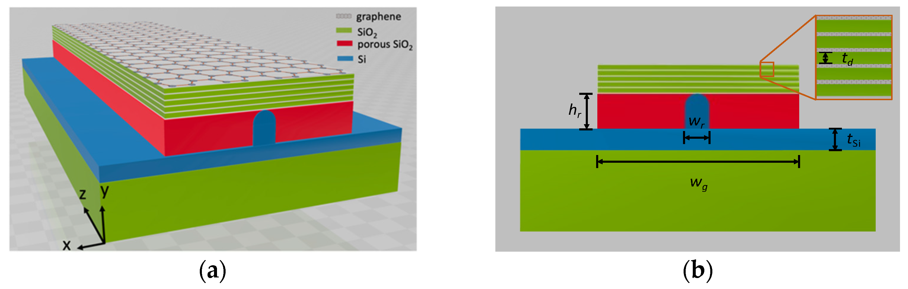
A 3D schematic diagram of the GPW and its front view are shown in Figure 1a,b, respectively. The structure consists of a porous SiO2 [46,47] layer sandwiched by MLGMTs, which are formed by alternating graphene–dielectric layers, and a Si nano-rib waveguide deposited on a conventional SiO2 substrate. Here, the same SiO2 as the substrate is chosen as the dielectric layers in the MLGMTs. Following the HPW structure [40], the MLGMTs, porous SiO2, and Si nano-rib are considered the metal, low-index dielectric, and high-index dielectric layers, respectively. Therefore, the mode field of the present structure can be strongly squeezed in the nanoscale region between the Si nano-rib and the MLGMTs, thus achieving ultrasmall mode sizes.
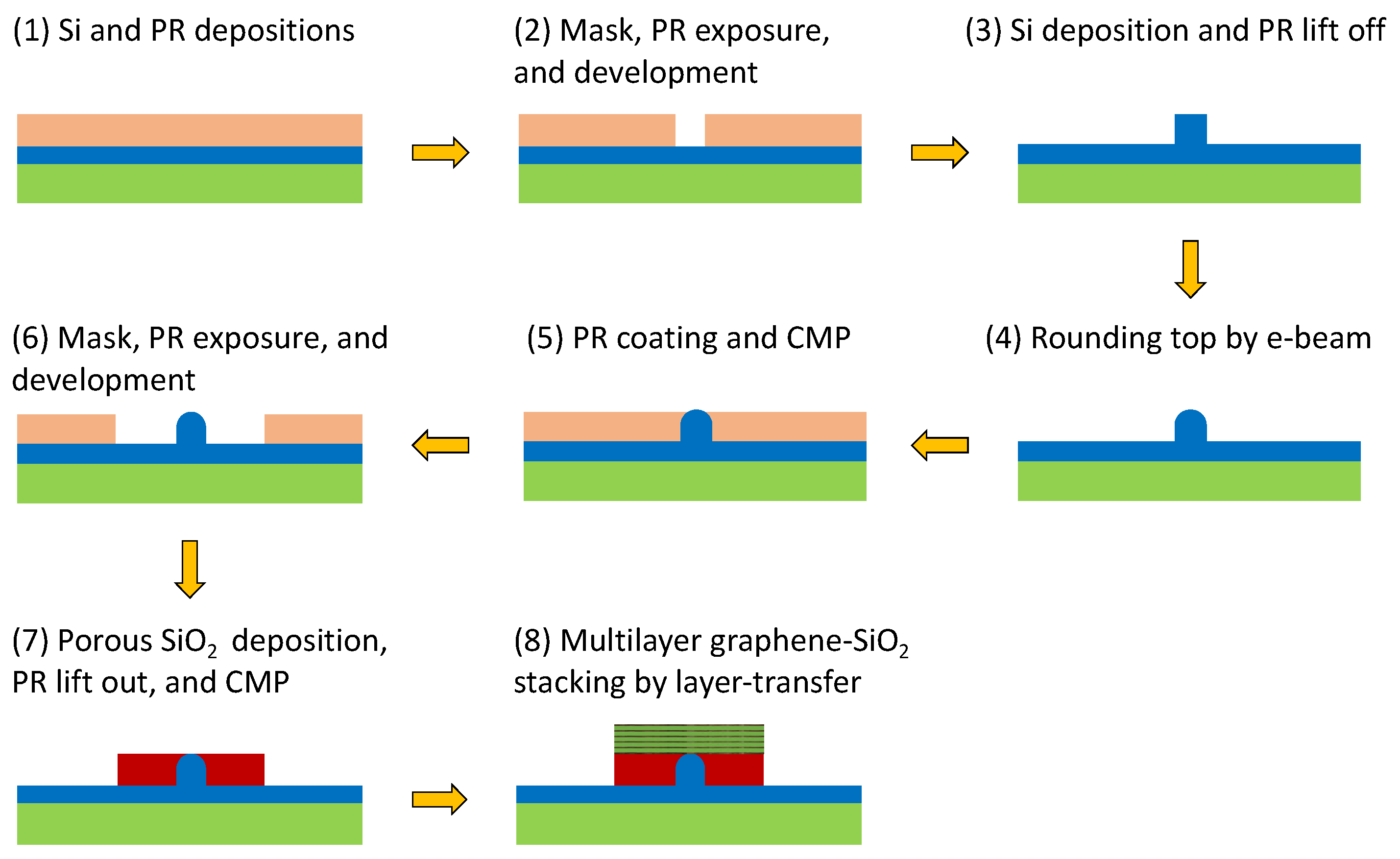
The fabrication steps are schematically shown in Figure 2 and are described as follows:
(1) Si and positive photoresist (PR) films with thickness hr (nm) are deposited on a conventional SiO2 substrate; (2) a mask is applied and followed by PR exposure and PR development to define a rectangular groove; (3) a Si layer is deposited and followed by the lift off of the PR to form a Si nano-rib waveguide; (4) the top of the Si nano-rib is rounded using e-beam lithography by carefully controlling the exposure time and scanning speed; (5) a PR film is coated on the surface and is used to flatten the PR film using chemical mechanical polishing (CMP); (6) a mask is applied and followed by PR exposure and PR development to lift out the PR film and define the porous SiO2 region; (7) a porous SiO2 film is evaporated on the surface using the oblique deposition technique [46,47], the PR film is lifted off, and then CMP is used to flatten the porous SiO2 layer; finally, (8) forming multilayer graphene–SiO2 stacking by a chemical vapor deposition (CVD), a layer transfer method [48,49,50], or transfer-free, solution-phase deposition method [51,52]. Considering the high-technique step to form the MLGMTs, we describe the main fabrication processes as follows. The former approaches [48,49,50] include depositing graphene on a copper foil, transferring it to the substrate using the PMMA transfer technique, etching the copper foil using ammonium persulfate, doping the graphene by soaking the sample in a suitable solution, depositing the target dielectric layer by the atomic layer deposition being able to carefully control its thickness, and finally repeating the processes to achieve the desired number of layers. Note that the number of graphene layers in [50] can reach 11 layers. For the latter approach [51,52], the fabrication processes include the use of graphene-oxide (GO) in solution, deposition directly on a dielectric layer without requiring a transfer process, repetition to achieve the desired number of GO layers, and finally laser photoreduction from GO to graphene with removing the oxygen-functional groups, in which the bandgap of the graphene can be tuned by varying the lase power. Note that the number of graphene layers in [52] can reach 20 layers. Compared to the CVD transfer method [48,49,50], the advantages of the solution-phase method [51,52] are transfer-free, with quality independent of the number of layers, and controllable for the optical responses by tunning the bandgap of graphene. Consequently, the fabrication of the multilayer graphene metamaterials may be not that challenging and have complex techniques required and is moderately achievable using modern fabrication techniques, making the proposed waveguide structure practically realizable. Note that the conventional electrical gating on graphene layers uses a single voltage to a top contact [53,54], thus resulting in an inhomogeneous chemical potential of the graphene layers varying from layer to layer due to interlayer screening [55] in a multilayer graphene structure. The non-uniformity of chemical potential is more significant as the number of graphene layers increases. As a result, a potential scheme [49] can be adopted to achieve the required chemical potential in the proposed MLGHPW. This approach controls the Fermi energy levels of individual graphene layers by different gate voltages, making the carrier concentrations alter together in all layers.
In theory, the MLGMTs can be considered a coupled system with interacting multiple graphene sheets supporting multiple nondegenerate plasmon modes (called VPP modes). The VPP modes show hyperbolic isofrequency contours [45] and a large density of electromagnetic states, resulting in high-k guided modes. Among the VPP modes, the fundamental VPP mode (VPP0) shows the lowest loss, although it possesses a comparably larger mode size. By coupling the VPP0 with the dielectric mode of the Si nano-rib waveguide, a hybrid mode not only preserves the low-loss property of the VPP0, but also significantly benefits from the high mode confinement of the Si nano-rib. In the present structure, the geometry parameters are as follows: wg and td are the width and thickness, respectively, of the dielectric (SiO2) layer; N is the number of MLGMT layers between graphene sheets (N + 1 layers); and wr, hr, and tSi are the width, height, and bottom thickness of the Si nano-rib waveguide, respectively. Here, we set the radius of curvature to r = wr/2. The relative permittivities of Si, conventional SiO2, and porous SiO2 at f = 20 THz are εSi = 12.25 [56], εSiO2 = 2.25 [56], and εp-SiO2 = 1.10 [46], respectively. Here, graphene is modeled as an infinitely thin sheet with a surface current density of J = σE in-plane, where E is the electric field vector and σ is the total surface conductivity of graphene with σ = σintra + σinter, including intraband (σintra) and interband (σinter) contributions, which can be calculated using the local random phase approximation [57]:
and
where EF is the Fermi energy, τ = µEF/eVF2 is the carrier relaxation lifetime, T is the temperature, kB is the Boltzmann constant, ℏ is the reduced Planck constant, e is the electron charge, µ is the carrier mobility in graphene, and VF = 106 m/s is the Fermi velocity of electrons. Here, we consider a carrier mobility, µ = 1 m2/V·s, at T = 300 K, which is also used to study the performance of GPWs [34,35,36,37,38,39]. To evaluate the waveguiding performance of plasmonic waveguides, the propagation length (Lp), FoM ( [40]), and normalized mode area (Am = Ae/A0) are used, where A0 = λ2/4 (λ is the working wavelength) is the diffraction-limited mode area and Ae is the effective mode area given by
Equation (3) includes the ratio of the total mode energy, Wm, and the peak of the energy density, W(r), which is given by:
where ω is the angular frequency, ε(r) is the profile of relative permittivity, µ0 is the permeability in a vacuum, and |E| and |H| are the intensities of the electric and magnetic fields, respectively. The numerical results are calculated using the COMSOL Multiphysics software based on the rigorous finite element method.
3. Results and Discussion
3.1. Waveguiding Performance Dependence on the Number of MLGMT Graphene Layers
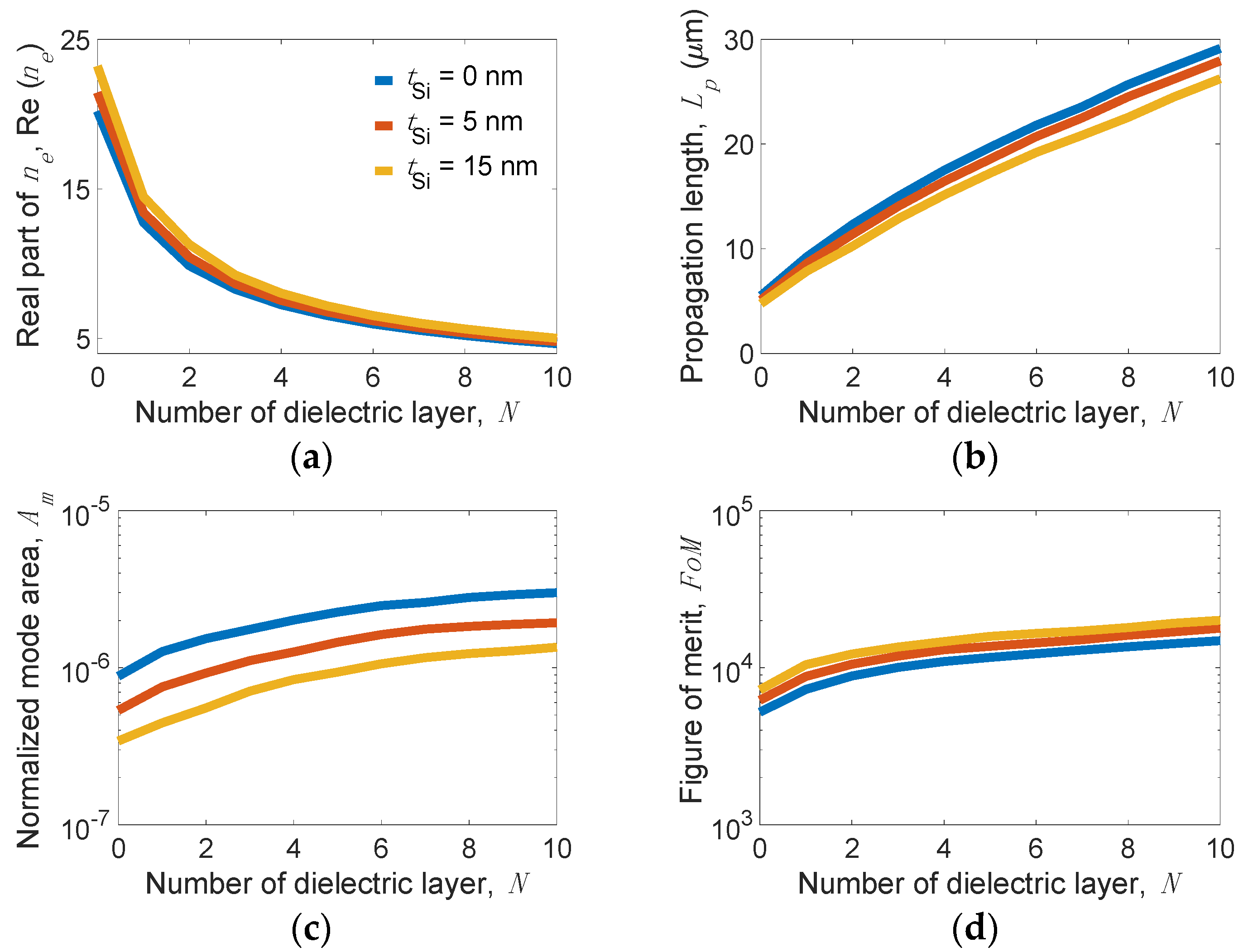
Figure 3 shows the mode properties of the present structure versus N for several values of tSi at the following parameters: wg = 200 nm, td = 5 nm, wr = 10 nm, hr = 30 nm, EF = 0.6 eV, and f = 20 THz. We observe that the real part of ne, Re(ne) sharply decreases from approximately 20 to 5 as N increases (see Figure 3a), but Am moderately increases from 5.34 × 10⁻⁷ to 1.93 × 10⁻⁶ for tSi = 5 nm (see Figure 3b). Note that the slopes of Re(ne) and Am versus N become smaller when N is greater than five, meaning that Re(ne) and Am are slightly influenced by larger N values. In contrast, Lp linearly increases from 5.1 to 27.9 µm for tSi = 5 nm as N increases from 0 to 10 (see Figure 3c). Further increasing Lp is only limited by the ability to fabricate an increasing number of N. The FoM increases from 6214 at N = 0 to 17,830 at N = 10 for tSi = 5 nm (see Figure 3d).
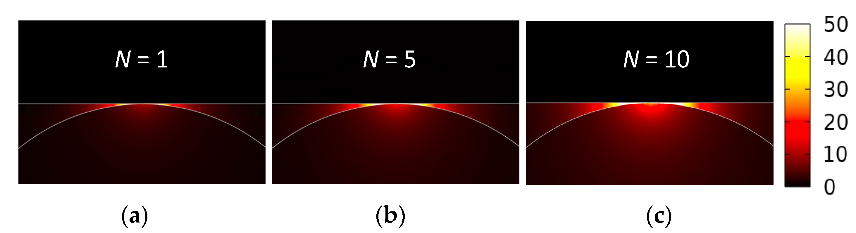
The obtained results show that the proposed design can achieve both an ultralong Lp (up to ~28 µm) and an extremely small Am (on the order of 10−6). Comparing these values with Am = 9.8 × 10⁻⁷ and Lp = 3.5 µm of the GCNWLSNR [39], the present structure improves Lp by more than three times while maintaining a comparable order of magnitude of Am. For observing the mode profiles, Figure 4a–c depict the |E| values near the nanoscale region between the MLGMTs and Si nano-rib for N = 1, 5, and 10 at tSi = 5 nm. Clearly, increasing N results in a stronger peak of |E| but looser mode confinement, leading to the moderate increase in Am (see Figure 3b).
Figure 5a,b also show 1D field plots along the horizontal dashed line H (inset of Figure 5a) and vertical dashed line V (inset of Figure 5b), respectively, to more clearly observe the relative mode profiles for different N values. The ultrasmall Am = 10−6 of the present design shows full widths at half maximums of approximately 1 and 0.1 nm along the x and y directions, respectively. The Lp can be attributed to the mode profile being significantly shifted from the region of MLGMTs to the Si nano-rib as N increases (see Figure 5b). Note that the conditions EF = 0.6 eV, N = 10, and f = 20 THz are used in subsequent analyses unless stated otherwise.
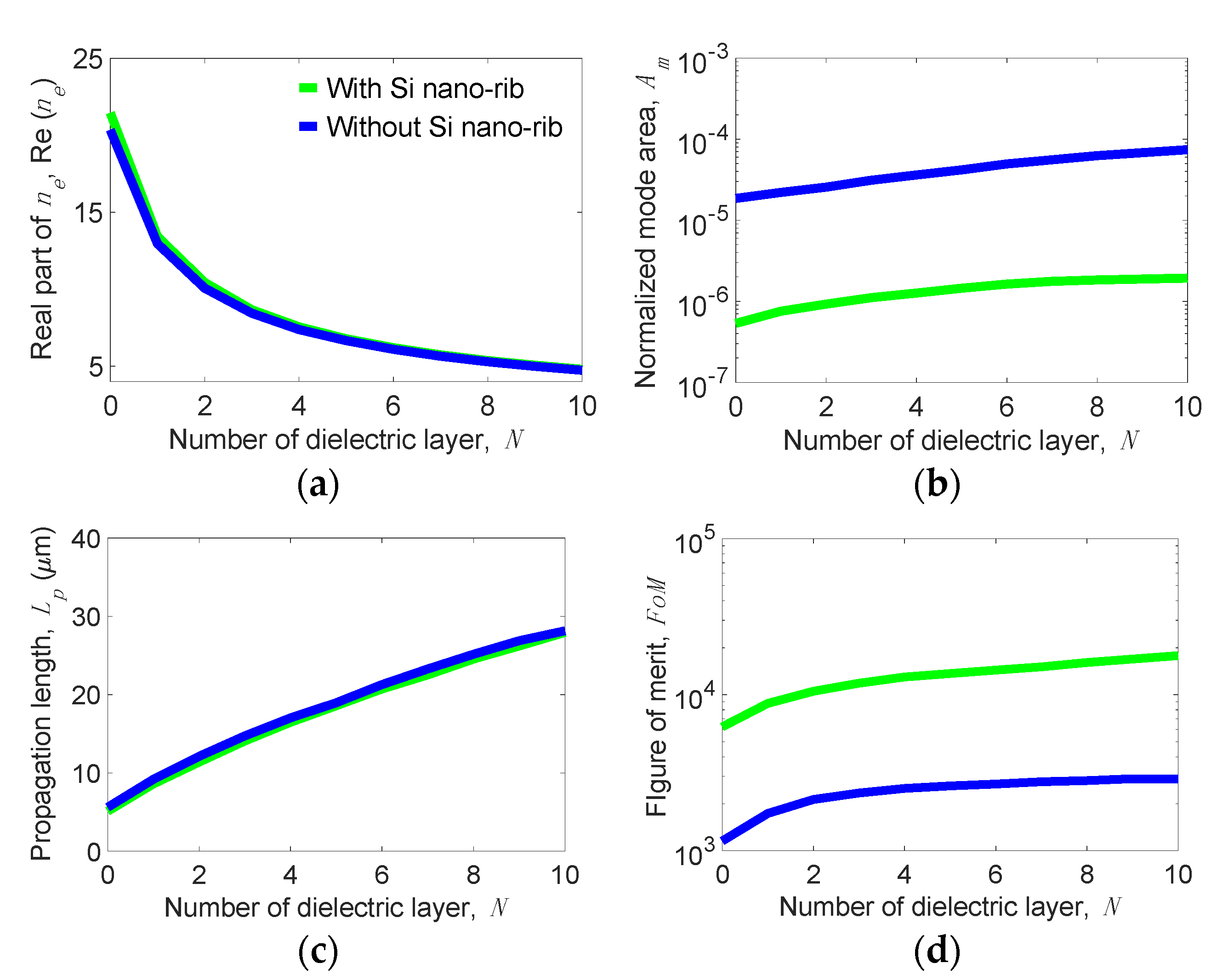
To clearly elucidate how the dielectric Si nano-rib changes the VPP0 mode, we analyze the properties of the VPP0 mode supported by the proposed structure without the nano-rib. Figure 6 shows the mode properties of the present structure with and without the nano-rib versus N at the same parameters as used in Figure 3 with tSi = 5 nm.
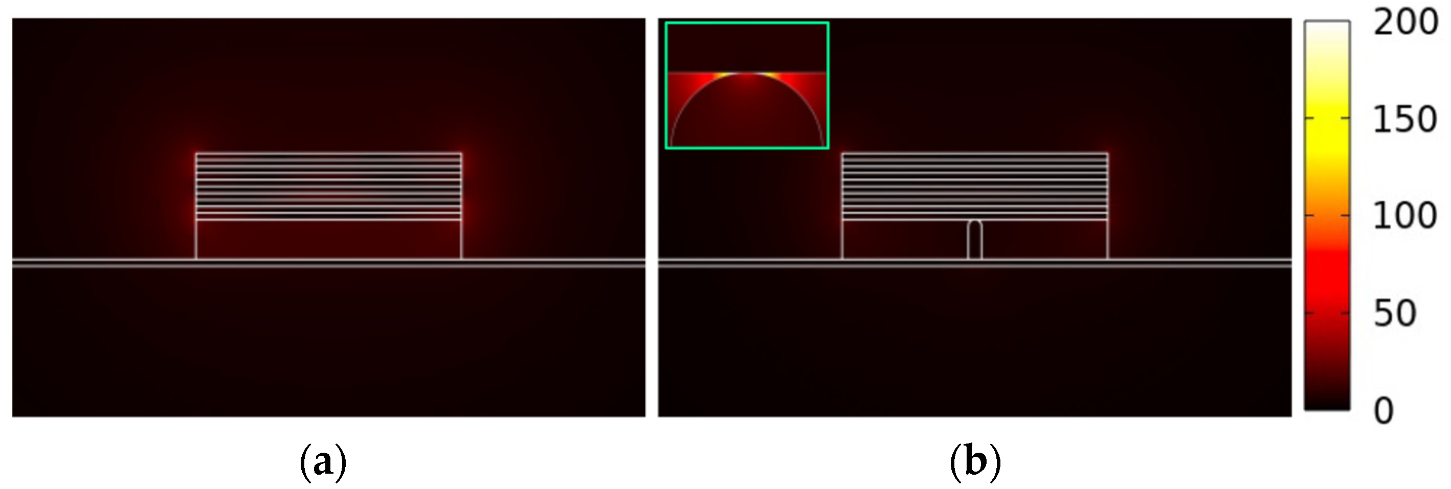
We observe that Re(ne) and Lp of the two structures are really close, but Am of the structure without the nano-rib is one to two orders of magnitude larger than that of the present structure as shown in Figure 6b, making the FoM of the structure without the nano-rib about one order of magnitude smaller. The above result reveals that the nano-rib can make the field distribution of the VPP0 mode significantly concentrated around the nanoscale region between the nano-rib and the MLGMTs. For observing the effect, Figure 7a,b show the |E| distributions of the present structure with and without the nano-rib, respectively, along with the zoomed-in view (see inset of Figure 7b) of the |E| distribution around the nano-rib. Without the nano-rib, the field profile spreads stronger out of the MLGMTs than that of the present design. In addition, the field of the present structure is significantly enhanced and focused mainly around the nano-rib, effectively shrinking its Am.
3.2. Mode Characteristic Dependence on Geometric Parameters
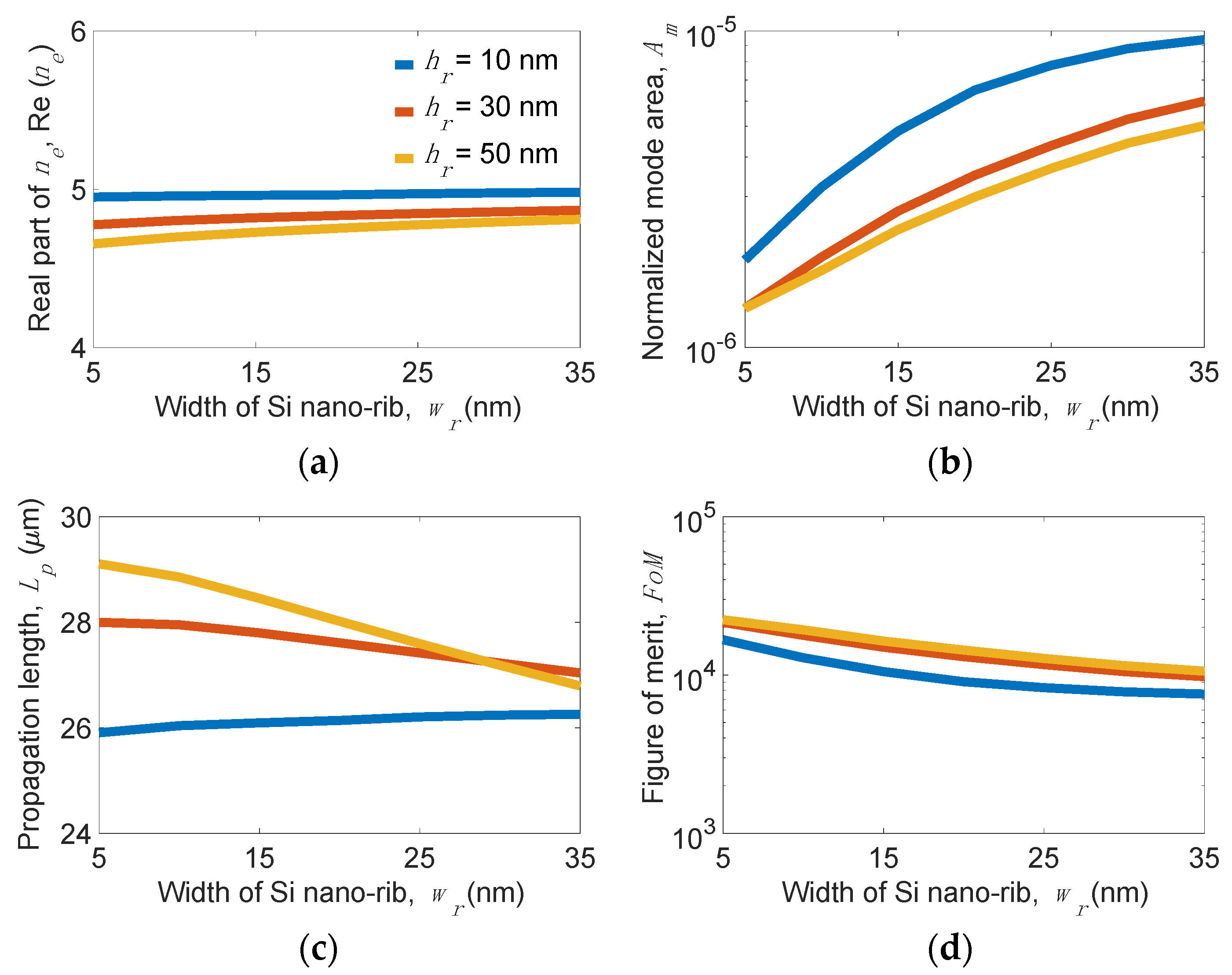
To fully assess the waveguiding performance of the proposed structure, we analyze the geometrical dependence of the mode properties. Figure 8 shows the mode properties versus wr for several hr values at wg = 200 nm, tSi = 5 nm, and td = 5 nm. We observe that Re(ne) slightly depends on wr and hr (see Figure 8a) but Am shows a substantial dependence on wr and hr (see Figure 8b). For example, Am varies from 1.6 × 10⁻⁶ to 6.0 × 10⁻⁶, while wr changes from 5 to 35 nm at hr = 30 nm. This effect can be attributed to a larger wr, obviously leading to a looser mode confinement. On the other hand, larger hr attains tighter Am due to the increase in the area of a low-index region, making the mode field more concentrated towards the region between the MLGMTs and the Si nano-rib. However, Lp significantly increases as hr increases, although Am shrinks. This is because the mode field shifts toward the Si nano-rib side as hr increases. Interestingly, Lp slightly increases for the smaller hr = 10 nm but moderately decreases for the larger hr > 30 nm as wr increases (see Figure 8c). For example, Lp varies from 29.2 (25.8) at wr = 5 nm to 26.8 (26.2) µm at wr = 35 nm for hr = 50 (10) nm. Note that smaller wr or larger hr (>20 nm here) can effectively improve the FoM of the proposed waveguide structure (see Figure 8d).
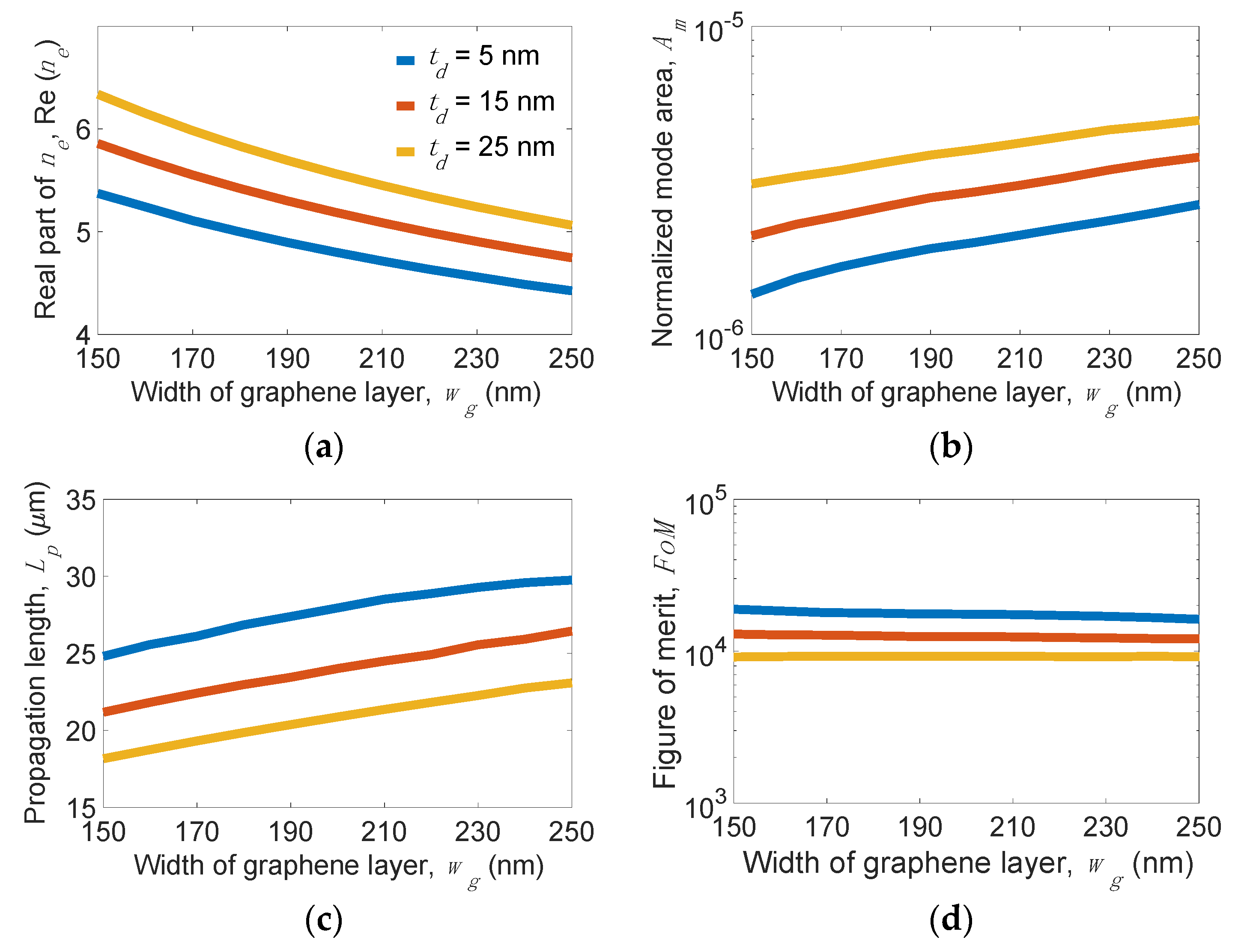
Next, we consider the effects of wg and td of the MLGMTs on mode properties. At wr = 10 nm, hr= 30 nm, and tSi= 5 nm, Figure 9 shows the mode properties versus wg for several td values. We observe that Re(ne), Am, and Lp moderately depend on wg and td. We also observe that Am and Lp decrease as wg decreases. Differing from increasing hr, which leads to a smaller Am (see Figure 8b), increasing wg increases Am, although they all increase the low-index region. This is because increasing wg also increases the width of the MLGMTs, leading to a looser mode field. The compensation between Am and Lp makes the FoM almost constant for different values of wg. As for the td, the smaller value leads to stronger coupling between SPP modes at individual graphene sheets. Therefore, smaller td concurrently achieves lower loss and smaller mode size, breaking the trade-off between Am and Lp to effectively improve the waveguiding performance of the proposed structure.
3.3. Fabrication Tolerance, Material Parameters of Graphene, and Spectral Response
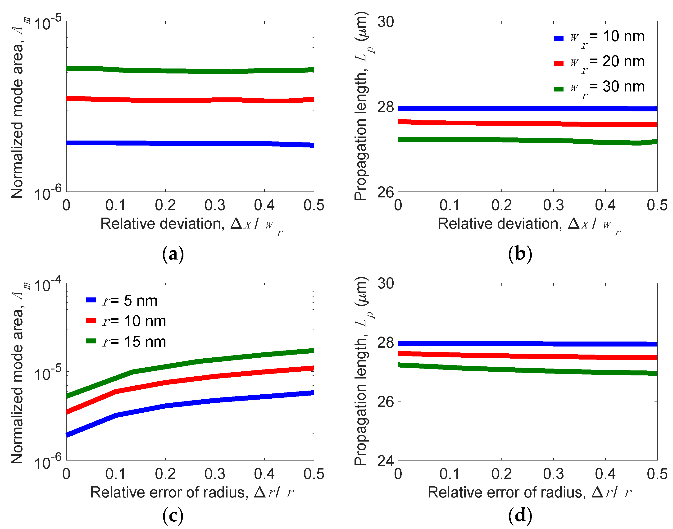
In experiments, fabrication imperfections lead to a reduction in waveguiding performance. Among the geometric parameters, the strictest part of the structure that should be precisely fabricated is the dimension of the Si nano-rib. Figure 10a,b show the dependence of Am and Lp on the relative fabrication error, Δx/wr, at hr = 30 nm, tSi = 5 nm, td = 5 nm, and wg = 200 nm, where Δx is the fabrication error. Evidently, Am and Lp are almost invariant in the range between Δx/wr = 0 and 0.5. Similarly, the dependence of Am and Lp on the relative fabrication error Δr/r, where Δr is the fabrication error, are shown in Figure 10c,d, respectively. At r = 10 nm, Am moderately varies from 4.2 × 10⁻⁶ to 8.5 × 10⁻⁶ while Δr/r deviates from 0 to 0.5, but Lp remains constant, although Δr/r = 0.5. The analyzed results verify that the proposed structure possesses high fabrication tolerance on mode properties.
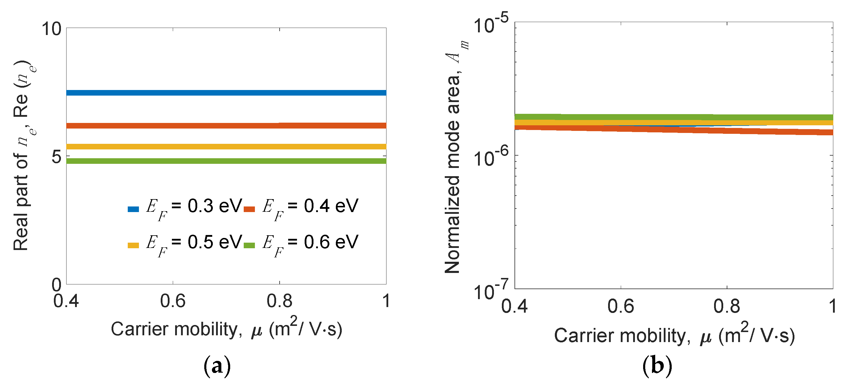
Considering a high doping level of graphene that leads to reducing the carrier mobility (µ), we investigated the mode properties versus µ for several EF’s, as shown in Figure 11. We observe that Re(ne) and Am are nearly independent on µ; however, Lp linearly reduces as µ decreases due to increasing the ohmic loss significantly for a higher doping level of EF > 0.5 eV. At EF = 0.4 eV, Lp varies from 10.7 to 7.4 µm at µ = 1 and 0.6 (m2/V·s), respectively. On the other hand, a lower EF attains a moderately higher Re(ne) and slightly smaller Am showing a tighter mode confinement, but significantly leads to a shorter Lp (see Figure 11c). For example, Lp varies from 19.5 to 10.8 µm at EF = 0.5 and 0.4 eV, respectively, for the condition µ = 1 (m2/V·s). The results reveal that a lower EF or µ leads to a reduction in Lp for general GPWs, mainly due to the higher ohmic losses.
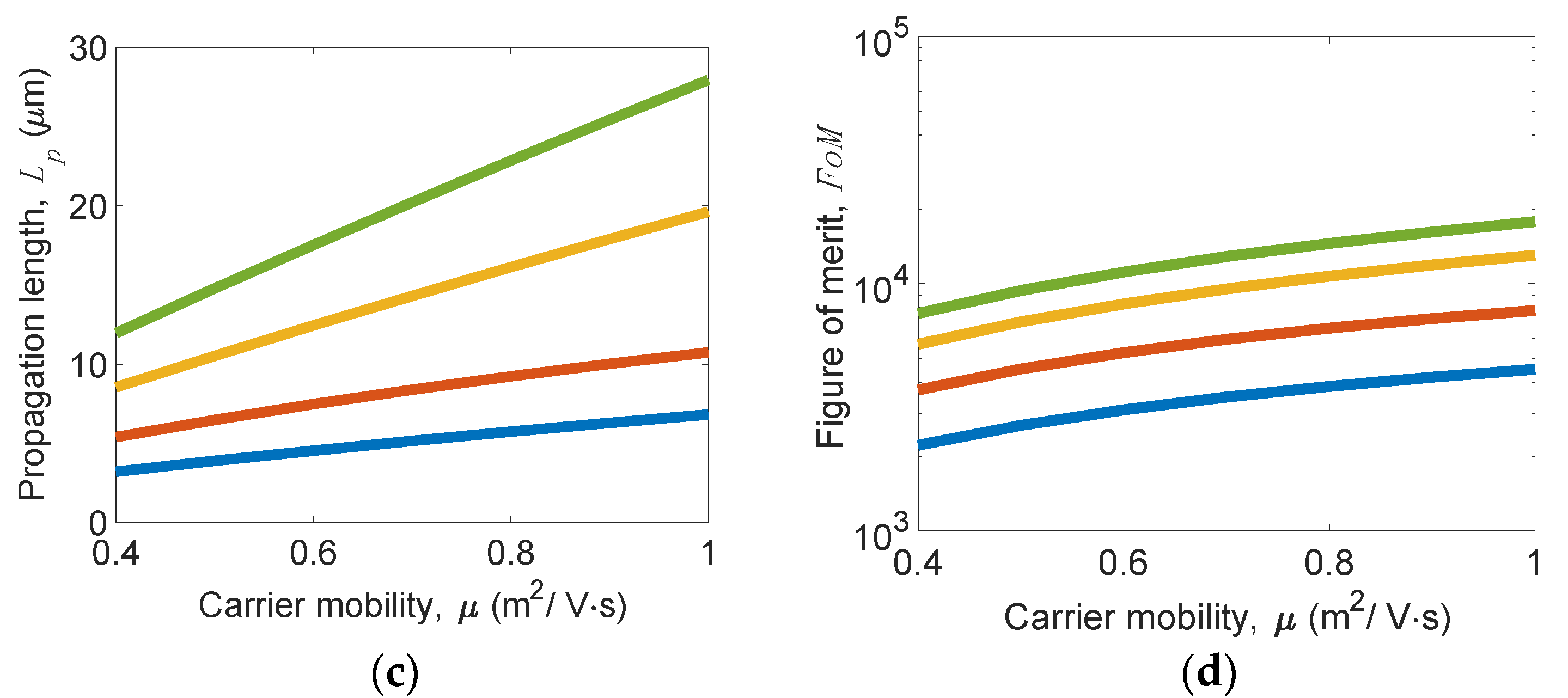
To fully study the tunability of graphene within a bandwidth range, we address the spectral response of mode properties. At wg = 200 nm, wr = 10 nm, hr = 30 nm, tSi = 5 nm, and td = 5 nm, the results for several values of EF are shown in Figure 12. As the working frequency, f, increases from 10 to 30 THz, Re(ne) and Am moderately increase, but Lp significantly decreases. Considering the effect of EF, Re(ne) increases, but Am and Lp decrease because of the enhanced mode localization as EF decreases. Note that Am is slightly influenced while Lp is significantly influenced by varying EF. At f = 10 (30) THz, our design achieves unprecedented long Lp values of 12.1 (4.8) and 38.9 (19.4) µm while maintaining ultrasmall Am values of 6.8 × 10⁻⁷ (1.8 × 10⁻⁶) and 7.8 × 10⁻⁷ (2.6 × 10⁻⁶) for EF = 0.4 and 0.6 eV, respectively. Exceptionally, the obtained FoM values are higher than 104 (3.0 × 10³) within f = 10–30 THz, even while operating at EF = 0.6 (0.3) eV.
The conventional electrical gating on graphene layers uses a single voltage to a top contact [50,51], thus resulting in an inhomogeneous chemical potential of the graphene layers varying from layer to layer due to interlayer screening [52] in a multilayer graphene structure. The non-uniformity of chemical potential is more significant as the number of graphene layers increases. As a result, a potential scheme [49] can be adopted to achieve the required chemical potential in the proposed MLGHPW. This approach controls the Fermi energy levels of individual graphene layers by different gate voltages, making the carrier concentrations alter together in all layers.
3.4. Waveguide Crosstalk
In addition to the size of Am, the crosstalk of the modes in adjacent waveguides complements to describe the degree of mode confinement and examines the feasibility for high integration of photonic integrated circuits. Figure 13 shows a coupled waveguide consisting of two parallel waveguides with a center-to-center separation s.
According to the coupled mode theory (CMT) [58], energy exchange between the adjacent waveguides is due to the field coupling of evanescent tails of two normal modes. To evaluate the coupling strength, the coupling length of a lossless coupled waveguide system Lc = λ/[2(ns − na)] determines the length required to completely transfer power from one waveguide to another, where ns and na are the ne of the symmetric and asymmetric modes, respectively. For a lossy waveguide system such as plasmonic waveguides, we adopted a more suitable criterion, the normalized coupling length Lc/Lave [59], which considers both the power attenuation and maximum power transfer to measure the crosstalk, where Lave is the average Lp of the symmetric and asymmetric modes. The maximum transfer power ρmax between waveguides is only a function of Lc/Lave, and the adjacent waveguides can be considered as nearly isolated (ρmax = 0.33%) if Lc/Lave > 10 is reached. This is because the transfer power from one channel to the other is relatively weak at the distance of Lave. At the frequency f = 30 THz and the geometry parameters of wg = 180 nm, wr = 20 nm, hr = 30 nm, tSi = 25 nm, and td = 25 nm, the results of Lc/Lave along with ρmax versus s at µ = 1 m2/V.s for several EFs are shown in Figure 14a and those at EF = 0.4 eV are shown in Figure 14b for several µs. The results show that decreasing EF or µ leads to weaker coupling strength, and the dependence of coupling strength on EF is stronger than that on µ. We observe that the separations for negligible couplings between waveguides are s = 0.52, 0.64, and 0.72 µm for EF = 0.35, 0.40, and 0.45 eV, respectively (see Figure 14a), and are s = 0.57, 0.61, and 0.64 µm for µ = 0.5, 0.75, and 1 m2/V.s, respectively (see Figure 14b). The results demonstrated that the coupling strength can be tuned by varying EF or µ, respectively. For instance, ρmax achieves about 20% at EF = 0.45 eV and 5% at EF = 0.35 eV for the condition µ = 1 m2/V.s and s = 0.4 µm. The small values of s (about 0.5 to 0.7 µm) make the proposed waveguide capable of building high-density graphene-based photonic-integrated circuits operating in the mid-infrared range.
3.5. Comparison of Waveguiding Performance
To demonstrate the superior waveguiding performance of the proposed design, we compared the reported results [32,34,36,38,39] in Table 1 with our mode properties at the following parameters: wg = 200 nm, wr = 10 nm, hr = 30 nm, tSi = 5 nm, td = 5 nm, EF = 0.6 eV, and N = 10. All the results in Table 1 were calculated at f = 30 THz, µ = 1 m2/V·s, and EF = 0.6 eV, except the results in ref. [32] with EF = 0.8 eV. If EF = 0.8 eV is decreased to 0.6 eV, Am and Lp will be further reduced. Liu et al. [32] achieved an extremely small area, Am = 8.0 × 10⁻⁷, by adopting a symmetrical HPW. Teng et al. [36] proposed a GCNW dimer to cause the coupling of the fundamental modes between two GCNWs to improve the Am of the single GCNW [34] by one order of magnitude while keeping the same Lp. Liu et al. [38] extended their previous report [32] to add an extra graphene sheet between Si and SiO2 layers and roll it into a cylindrical waveguide. It can be inferred that the two-layer graphene structure effectively improves the Lp but at the cost of a larger Am. Last year, Teng et al. [39] proposed a GCNWLSNR structure composed of a single GCNW deposited on a Si nano-rib, which showed a performance of Lp = 3.5 µm and Am = 2.0 × 10⁻⁶. In comparison with these published results [32,34,36,38,39], the proposed structure achieves an unprecedented waveguiding performance of Lp = 19.4 µm and Am = 2.6 × 10⁻⁶, thus obtaining an extremely high value of FoM = 10,612.
Currently, the obstacles for experimentally fabricating integrated graphene waveguides include three major points, despite the mature developments of both silicon photonics and graphene industries. (1) Excitation of extremely high-k SPP modes supported by monolayer graphene; (2) high-efficiency coupling between the nanoscale mode sizes of high-k SPP modes and submicron-scale dielectric waveguide modes or micron-scale optical fiber modes; (3) sufficient long propagation length beyond hundreds of micrometers or even millimeters. To relieve the first obstacle, employing multilayer graphene structures can efficiently control the field localizations and effective refractive index by varying the number of the graphene layers, thus overcoming the difficulty of exciting the high-k SPP modes. Next, the coupling efficiency can be improved by designing perfectly adiabatic metallic gratings, reducing field scattering during the coupling process. The final one is a common limit, as the SPP modes supported by general noble metals operating in the near-IR and visible light bands. In addition to discovering new low-loss materials, designing a novel waveguide structure by combining multiple guiding mechanisms together has been the most effective solution to decrease the propagation losses.
4. Conclusions
This work reported a mid-IR waveguiding structure based on MLGMTs on a Si nano-rib waveguide structure covered by a porous SiO2 layer. By coupling the low-loss fundamental VPP mode of the MLGMTs, which is formed by coupling the SPP modes at individual graphene sheets and the dielectric mode of a Si nano-rib, the hybrid mode of the present design achieves an ultralong propagation length Lp = 19.4 µm with Am = 2.6 × 10⁻⁶ at EF = 0.6 eV operating at f = 30 THz. Compared with the reported results, the Lp of our structure is five times greater than those reported at a comparable Am. Even for the looser Am, previously reported Lp values at EF = 0.6 eV and f = 30 THz were still limited to below 10 µm. The MLGMTs provide a high-conductivity graphene structure that significantly increases Lp with an increasing number of graphene layers. Therefore, the increased degree of Lp is mainly restricted by the modern fabrication technique. In addition, the crosstalk between two adjacent waveguides demonstrates that the proposed structure is beneficial in realizing high-integration photonic devices operating in the mid-IR band. Our design is expected to pave the way for potential applications in building ultralow loss and compact and tunable mid-IR photonic devices and can be extended to other extraordinary 2D materials.
Author Contributions
All authors conceived the designed idea and discussed the results. R.-J.C. and C.-W.C. performed the numerical simulations. C.-C.H. wrote the manuscript and supervised the whole work. All authors have read and agreed to the published version of the manuscript.
Funding
This research was funded by the Ministry of Science and Technology (MOST) of Taiwan for financially supporting this research under grant number 110-2112-M-005-005.
Institutional Review Board Statement
Not applicable.
Informed Consent Statement
Not applicable.
Data Availability Statement
The data presented in this study are available on request from the corresponding author.
Acknowledgments
The authors would like to thank Yen-Fu Lin in the Institute of Nanoscience, National Chung Hsing University, for the insight discussions of the fabrication processes of multilayer graphene metamaterials.
Conflicts of Interest
The authors declare no conflict of interest.
References
- Barnes, W.L.; Dereux, A.; Ebbesen, T.W. Surface plasmon subwavelength optics. Nature 2003, 424, 824–830. [Google Scholar] [CrossRef]
- Gramotnev, D.K.; Bozhevolnyi, S.I. Plasmonics beyond the diffraction limit. Nat. Photonics 2010, 4, 83–91. [Google Scholar] [CrossRef]
- Han, Z.; Bozhevolnyi, S.I. Radiation guiding with surface plasmon polaritons. Rep. Prog. Phys. 2013, 76, 016402. [Google Scholar] [CrossRef]
- Bian, Y.; Gong, Q. Highly confined guiding of low-loss plasmon waves in hybrid metal-dielectric slot waveguides. Nanotechnology 2014, 25, 345201. [Google Scholar] [CrossRef]
- Bian, Y.; Ren, Q.; Kang, L.; Yue, T.; Werner, P.L.; Werner, D.H. Deep-subwavelength light transmission in hybrid nanowire-loaded silicon nano-rib waveguides. Photonics Res. 2018, 6, 37–45. [Google Scholar] [CrossRef] [Green Version]
- Stanley, R. Plasmonics in the mid-infrared. Nat. Photonics 2012, 6, 409–411. [Google Scholar] [CrossRef]
- Zhong, Y.; Malagari, S.D.; Hamilton, T.; Wasserman, D.M. Review of mid-infrared plasmonic materials. J. Nanophotonics 2015, 9, 093791. [Google Scholar] [CrossRef] [Green Version]
- Grigorenko, A.N.; Polini, M.; Novoselov, K.S. Graphene plasmonics. Nat. Photonics 2012, 6, 749–758. [Google Scholar] [CrossRef]
- Low, T.; Avouris, P. Graphene plasmonic for terahertz to mid-infrared applications. ACS Nano 2014, 8, 1086–1101. [Google Scholar] [CrossRef] [PubMed] [Green Version]
- Politano, P.; Chiarello, G. Plasmon modes in graphene: Status and prospect. Nanoscale 2014, 6, 10927–10940. [Google Scholar] [CrossRef] [PubMed]
- Gon, P.A.D.; Peres, N.M.R. An Introduction to Graphene Plasmonics; World Scientific: Singapore, 2016. [Google Scholar]
- Li, Y.; Tantiwanichapan, K.; Swan, A.K.; Paiella, R. Graphene plasmonic devices for terahertz optoelectronics. Nanophotonics 2020, 9, 1901–1920. [Google Scholar] [CrossRef]
- Bao, Q.; Zhang, H.; Wang, B.; Ni, Z.; Haley, C.; Lim, Y.X.; Wang, Y.; Tang, D.Y.; Loh, K.P. Broadband graphene polarizer. Nat. Commun. 2011, 5, 411–415. [Google Scholar] [CrossRef]
- Pei, C.; Yang, L.; Wang, G.; Wang, Y.; Jiang, X.; Hao, Y.; Li, Y.; Yang, J. Broadband graphene/glass hybrid waveguide polarizer. IEEE Photonics Technol. Lett. 2015, 27, 927–930. [Google Scholar] [CrossRef]
- He, X.; Liu, J. Flexible and broadband graphene polarizer based on surface silicon-core microfiber. Opt. Mater. Express 2017, 7, 1398–1405. [Google Scholar] [CrossRef]
- Kim, J.T.; Choi, H. Polarization control in graphene-based polymer waveguide polarizer. Laser Photonics Rev. 2018, 12, 1800142. [Google Scholar] [CrossRef]
- Liu, M.; Yin, X.; Ulin-Avila, E.; Geng, B.; Zentgraf, T.; Ju, L.; Wang, F.; Zhang, X. A graphene-based broadband optical modulator. Nature 2011, 474, 64–67. [Google Scholar] [CrossRef]
- Youngblood, N.; Anugrah, Y.; Ma, R.; Koester, S.K.; Li, M. Multifunctional graphene optical modulator and photodetector integrated on silicon waveguides. Nano Lett. 2014, 14, 2741–2746. [Google Scholar] [CrossRef] [Green Version]
- Ansell, D.; Radko, I.P.; Han, Z.; Rodriguez, F.J.; Bozhevolnyi, S.I.; Grigorenko, A.N. Hybrid graphene plasmonic waveguide modulators. Nat. Commun. 2015, 6, 8846. [Google Scholar] [CrossRef]
- Hao, R.; Jiao, J.; Peng, X.; Zhen, Z.; Dagarbek, R.; Zou, Y.; Li, E. Experimental demonstration of a graphene-based hybrid plasmonic modulator. Opt. Lett. 2019, 44, 2586–2589. [Google Scholar] [CrossRef]
- Ding, Y.; Guan, X.; Zhu, X.; Hu, H.; Bozhevolnyi, S.I.; Oxenløwe, L.K.; Jin, K.J.; Mortensen, N.A.; Xiao, S. Efficient electro-optic modulation in low-loss graphene-plasmonic slot waveguides. Nanoscale 2017, 9, 15576–15581. [Google Scholar] [CrossRef] [Green Version]
- Yuana, W.; Shi, G. Graphene-based gas sensors. J. Mater. Chem. A 2013, 1, 10078–10091. [Google Scholar] [CrossRef]
- Peters, A.; Turvey, S.; Horsfall, A.B. High-temperature Hall effect sensor based on epitaxial graphene on high-purity semiinsulating 4H-SiC. IEEE Trans. Electron Dev. 2019, 66, 3134–3138. [Google Scholar]
- Choi, J.H.; Lee, J.; Byeon, M.; Hong, T.E.; Park, H.; Lee, C.Y. Graphene-based gas sensors with high sensitivity and minimal sensor-to-sensor variation. ACS Appl. Nano Mater. 2020, 3, 2257–2265. [Google Scholar] [CrossRef]
- Ghorbanzadeh, M.; Darbari, S.; Moravvej-Farshia, M.K. Graphene-based plasmonic force switch. Appl. Phys. Lett. 2016, 108, 111105. [Google Scholar] [CrossRef]
- Dolleman, R.J.; Belardinelli, P.; Houri, S.; van der Zant, H.S.J.; Alijani, F.; Steeneken, P.G. High-frequency stochastic switching of graphene resonators near room temperature. Nano Lett. 2019, 19, 1282–1288. [Google Scholar] [CrossRef] [PubMed] [Green Version]
- Cox, J.D.; de Abajo, F.J.G. Single-plasmon thermo-optical switching in graphene. Nano Lett. 2019, 19, 3743–3750. [Google Scholar] [CrossRef] [PubMed]
- Ono, M.; Hata, M.; Tsunekawa, M.; Nozaki, K.; Sumikura, H.; Chiba, H.; Notomi, M. Ultrafast and energy-efficient all-optical switching with graphene-loaded deep-subwavelength plasmonic waveguides. Nat. Photonics 2020, 14, 37–43. [Google Scholar] [CrossRef] [Green Version]
- Ye, L.; Sui, K.; Feng, H. High-efficiency couplers for graphene surface plasmon polaritons in the mid-infrared region. Opt. Lett. 2020, 45, 264–267. [Google Scholar] [CrossRef]
- Sun, Y.; Bian, Y.; Zhao, X.; Zheng, Z.; Liu, J.; Liu, J. Low-loss graphene plasmonic waveguide based on a high-index dielectric wedge for tight optical confinement. In Proceedings of the OSA Technical Digest (Optical Society of America, 2013), online, 9–14 June 2013; p. JTu4A.33. [Google Scholar]
- Xu, W.; Zhu, Z.H.; Liu, K.; Zhang, J.F.; Yuan, X.D.; Lu, Q.S.; Qin, S.Q. Dielectric loaded graphene plasmon waveguide. Opt. Express 2015, 23, 5147–5153. [Google Scholar] [CrossRef]
- Liu, J.P.; Zhai, X.; Wang, L.L.; Li, H.J.; Xie, F.; Xia, S.X.; Shang, X.J.; Luo, X. Graphene-based long-range SPP hybrid waveguide with ultra-long propagation length in mid-infrared range. Opt. Express 2016, 24, 5376–5386. [Google Scholar] [CrossRef]
- Bahadori-Haghighi, S.; Ghayour, R.; Sheikhi, M.H. Design and analysis of low loss plasmonic waveguide and directional coupler based on pattern-free suspended graphene sheets. Carbon 2018, 129, 653–660. [Google Scholar] [CrossRef]
- Gao, Y.; Ren, G.; Zhu, B.; Wang, J.; Jian, S. Single-mode graphene-coated nanowire plasmonic waveguide. Opt. Lett. 2014, 39, 5909–5912. [Google Scholar] [CrossRef]
- Gao, Y.; Ren, G.; Zhu, B.; Liu, H.; Lian, Y.; Jian, S. Analytical model for plasmon modes in graphene-coated nanowire. Opt. Express 2014, 22, 24322–24331. [Google Scholar] [CrossRef]
- Teng, D.; Wang, K.; Li, Z.; Zhao, Y. Graphene-coated nanowire dimers for deep subwavelength waveguiding in mid-infrared range. Opt. Express 2019, 27, 12458–12469. [Google Scholar] [CrossRef] [PubMed]
- Liu, J.P.; Zhai, X.; Wang, L.L.; Li, H.J.; Xie, F.; Lin, Q.; Xia, S.X. Analysis of mid-infrared surface plasmon modes in a graphene-based cylindrical hybrid waveguide. Plasmonics 2016, 11, 703–711. [Google Scholar] [CrossRef]
- Liu, J.P.; Zhai, X.; Xie, F.; Wang, L.L.; Xia, S.X.; Li, H.J.; Luo, X.; Shang, X.J. Analytical model of mid-infrared surface plasmon modes in a cylindrical long-range waveguide with double-layer graphene. J. Lightwave Technol. 2017, 35, 1971–1979. [Google Scholar] [CrossRef]
- Teng, D.; Wang, K.; Huan, Q.; Chen, W.; Li, Z. High-performance light transmission based on graphene plasmonic waveguides. J. Mater. Chem. C 2020, 8, 6832–6838. [Google Scholar] [CrossRef]
- Oulton, R.F.; Sorger, V.J.; Genov, D.; Pile, D.; Zhang, X. A hybrid plasmonic waveguide for subwavelength confinement and long-range propagation. Nat. Photonics 2008, 2, 496–500. [Google Scholar] [CrossRef] [Green Version]
- Chen, B.; Meng, C.; Yang, Z.; Li, W.; Lin, S.; Gu, T.; Guo, X.; Wang, D.; Yu, S.; Wong, C.W. Graphene coated ZnO nanowire optical waveguides. Opt. Express 2014, 22, 24276–24285. [Google Scholar] [CrossRef] [PubMed]
- Cao, T.; Tian, L.; Liang, H.; Qin, K.R. Reconfigurable, graphene-coated, chalcogenide nanowires with a sub-10-nm enantioselective sorting capability. Microsyst. Nanoeng. 2018, 4, 7. [Google Scholar] [CrossRef] [Green Version]
- Iorsh, I.V.; Mukhin, I.S.; Shadrivov, I.V.; Belov, P.A.; Kivshar, Y.S. Hyperbolic metamaterials based on multilayer graphene structures. Phys. Rev. B 2013, 87, 075416. [Google Scholar] [CrossRef] [Green Version]
- Othman, M.A.K.; Guclu, C.; Capolino, F. Graphene-based tunable hyperbolic metamaterials and enhanced near-field absorption. Opt. Express 2013, 21, 7614–7632. [Google Scholar] [CrossRef] [PubMed] [Green Version]
- Smirnova, D.A.; Iorsh, I.V.; Shadrivov, I.V.; Kivshar, Y.S. Multilayer graphene waveguides. JETH Lett. 2014, 99, 456. [Google Scholar] [CrossRef] [Green Version]
- Schubert, E.F.; Kim, J.K.; Xi, J.Q. Low-refractive-index materials: A new class of optical thin-film materials. Phys. Status Solidi B 2007, 244, 3002–3008. [Google Scholar] [CrossRef]
- Lin, J.Y.; Liu, W.; Smart, J.A. Optical thin-film materials with low refractive index for broadband elimination of Fresnel reflection. Nat. Photonics 2007, 1, 176–179. [Google Scholar]
- Yan, H.; Li, X.; Chandra, B.; Tulevski, G.; Wu, Y.; Freitag, M.; Zhu, W.; Avouris, P.; Xia, F. Tunable infrared plasmonic devices using graphene/insulator stacks. Nat. Nanotechnol. 2012, 7, 330–334. [Google Scholar] [CrossRef] [Green Version]
- Chang, Y.C.; Liu, C.H.; Liu, C.H.; Zhang, S.; Marder, S.R.; Narimanov, E.E.; Zhong, Z.; Norris, T.B. Realization of mid-infrared graphene hyperbolic metamaterials. Nat. Commun. 2015, 7, 10568. [Google Scholar] [CrossRef] [PubMed] [Green Version]
- Baitimirova, M.; Viter, R.; Andzane, J.; Lee, A.; Voiry, D.; Iatsunskyi, I.; Coy, E.; Mikoliunaite, L.; Tumenas, S.; Załęski, K.; et al. Tuning of structural and optical properties of graphene/ZnO nanolaminates. J. Phys. Chem. C 2016, 120, 23716–23725. [Google Scholar] [CrossRef]
- Yang, Y.; Lin, H.; Zhang, B.Y.; Zhang, Y.; Zheng, X.; Yu, A.; Hong, M.; Jia, B. Graphene-based multilayered metamaterials with phototunable architecture for on-chip photonic devices. ACS Photonics 2019, 6, 1033–1040. [Google Scholar] [CrossRef]
- Lin, H.; Sturmberg, B.C.P.; Lin, K.; Yang, Y.; Zheng, X.; Chong, T.K.; Martijn de Sterke, C.; Jia, B. A 90-nm-thick graphene metamaterial for strong and extremely broadband absorption of unpolarized light. Nat. Photonics 2019, 13, 270–276. [Google Scholar] [CrossRef]
- Lee, C.C.; Suzuki, S.; Xie, W.; Schibli, T.R. Broadband graphene electro-optic modulators with sub-wavelength thickness. Opt. Express 2012, 20, 5264–5269. [Google Scholar] [CrossRef] [PubMed]
- Fan, M.; Yang, H.; Zheng, P.; Hu, G.; Yun, B.; Cui, Y. Multilayer graphene electro-absorption optical modulator based on double-stripe silicon nitride waveguide. Opt. Express 2017, 25, 21619–21629. [Google Scholar] [CrossRef] [PubMed]
- Sun, D.; Divin, C.; Berger, C.; De Heer, W.A.; First, P.N.; Norris, T.B. Spectroscopic measurement of interlayer screening in multilayer epitaxial graphene. Phys. Rev. Lett. 2010, 104, 136802. [Google Scholar] [CrossRef] [PubMed] [Green Version]
- Bass, M.; DeCusatis, C.; Enoch, J.; Lakshminarayanan, V.; Li, G.; MacDonald, C.; Mahajan, V.; StrylandBass, E.V. Handbook of Optics, Third Edition Volume IV: Optical Properties of Materials, Nonlinear Optics, Quantum Optics; McGraw-Hill: New York, NY, USA, 2009. [Google Scholar]
- Falkovsky, L.A.; Pershoguba, S.S. Optical far-infrared properties of a graphene monolayer and multilayer. Phys. Rev. B 2007, 76, 153410. [Google Scholar] [CrossRef] [Green Version]
- Huang, W.P. Coupled-mode theory for optical waveguides: An overview. J. Opt. Soc. Am. A 1994, 11, 963–983. [Google Scholar] [CrossRef]
- Veronis, G.; Fan, S.H. Crosstalk between three-dimensional plasmonic slot waveguides. Opt. Express 2008, 16, 2129–2140. [Google Scholar] [CrossRef] [Green Version]
Figure 1.
Schematic of the proposed waveguide structure—(a) 3D structure and (b) cross section of (a) with a zoomed-in view of the MLGMTs.
Figure 1.
Schematic of the proposed waveguide structure—(a) 3D structure and (b) cross section of (a) with a zoomed-in view of the MLGMTs.

Figure 2.
Schematic of the fabrication process for the proposed waveguide structure.

Figure 3.
(a) Real part of effective index ne, Re(ne), (b) normalized mode area, Am, (c) propagation length, Lp, and (d) figure of merit, FoM versus the number of dielectric layer, N for the present structure operating at f = 20 THz for different tSi values at parameters of wg = 200 nm, td = 5 nm, wr = 10 nm, hr = 30 nm, and EF = 0.6 eV.

Figure 4.
Mode fields of |E| for N = (a) 1, (b) 5, and (c) 10 at the same parameters as in Figure 3.
Figure 4.
Mode fields of |E| for N = (a) 1, (b) 5, and (c) 10 at the same parameters as in Figure 3.

Figure 5.
Electric fields, |E| along the (a) horizontal dashed line H and (b) vertical dashed line V shown in the corresponding insets for N = 1, 5, and 10.
Figure 5.
Electric fields, |E| along the (a) horizontal dashed line H and (b) vertical dashed line V shown in the corresponding insets for N = 1, 5, and 10.

Figure 6.
(a) Real part of effective index ne, Re(ne), (b) normalized mode area, Am, (c) propagation length, Lp, and (d) figure of merit, FoM versus the number of dielectric layer N for the present structure with and without the Si nano-rib.
Figure 6.
(a) Real part of effective index ne, Re(ne), (b) normalized mode area, Am, (c) propagation length, Lp, and (d) figure of merit, FoM versus the number of dielectric layer N for the present structure with and without the Si nano-rib.

Figure 7.
Mode fields of |E| for the present waveguide structure (a) without and (b) with the Si nano-rib.
Figure 7.
Mode fields of |E| for the present waveguide structure (a) without and (b) with the Si nano-rib.

Figure 8.
(a) Real part of effective index ne, Re(ne), (b) normalized mode area, Am, (c) propagation length, Lp, and (d) figure of merit, FoM of the present structure versus the width of Si nano-rib, wr for different height of Si nano-rib, hr values at the width of MLGMTs, wg = 200 nm, thickness of the bottom Si layer, tSi = 5 nm, and thickness of dielectric layers of MLGMTs, td = 5 nm.

Figure 9.
(a) Real part of effective index ne, Re(ne), (b) normalized mode area, Am, (c) propagation length, Lp, and (d) figure of merit, FoM, of the present structure versus wg for different td values at wr = 10 nm, hr = 30 nm, and tSi = 5 nm.
Figure 9.
(a) Real part of effective index ne, Re(ne), (b) normalized mode area, Am, (c) propagation length, Lp, and (d) figure of merit, FoM, of the present structure versus wg for different td values at wr = 10 nm, hr = 30 nm, and tSi = 5 nm.

Figure 10.
Dynamics of (a) normalized mode area, Am, and (b) propagation length, Lp, versus the relative fabrication error of the width of the Si nano-rib (Δx/wr) for different wr values; (c) Am and (d) Lp versus the relative fabrication error of the radius of the curvature of the Si nano-rib (Δr/r) for different r values when hr = 30 nm, tSi = 5 nm, td = 5 nm, and wg = 200 nm.

Figure 11.
Plots of (a) real part of effective index ne, Re(ne), (b) normalized mode area, Am, (c) propagation length, Lp, and (d) figure of merit, FoM, of the present structure versus carrier mobility, µ, for several EF’s at wg = 200 nm, wr = 10 nm, hr = 30 nm, tSi = 5 nm, td = 5 nm, and f = 20 THz.


Figure 12.
Plots of (a) real part of effective index ne, Re(ne), (b) normalized mode area, Am, (c) propagation length, Lp, and (d) figure of merit, FoM, of the present structure versus the operating frequency, f, for several values of EF when wg = 200 nm, wr = 10 nm, hr = 30 nm, tSi = 5 nm, and td = 5 nm.

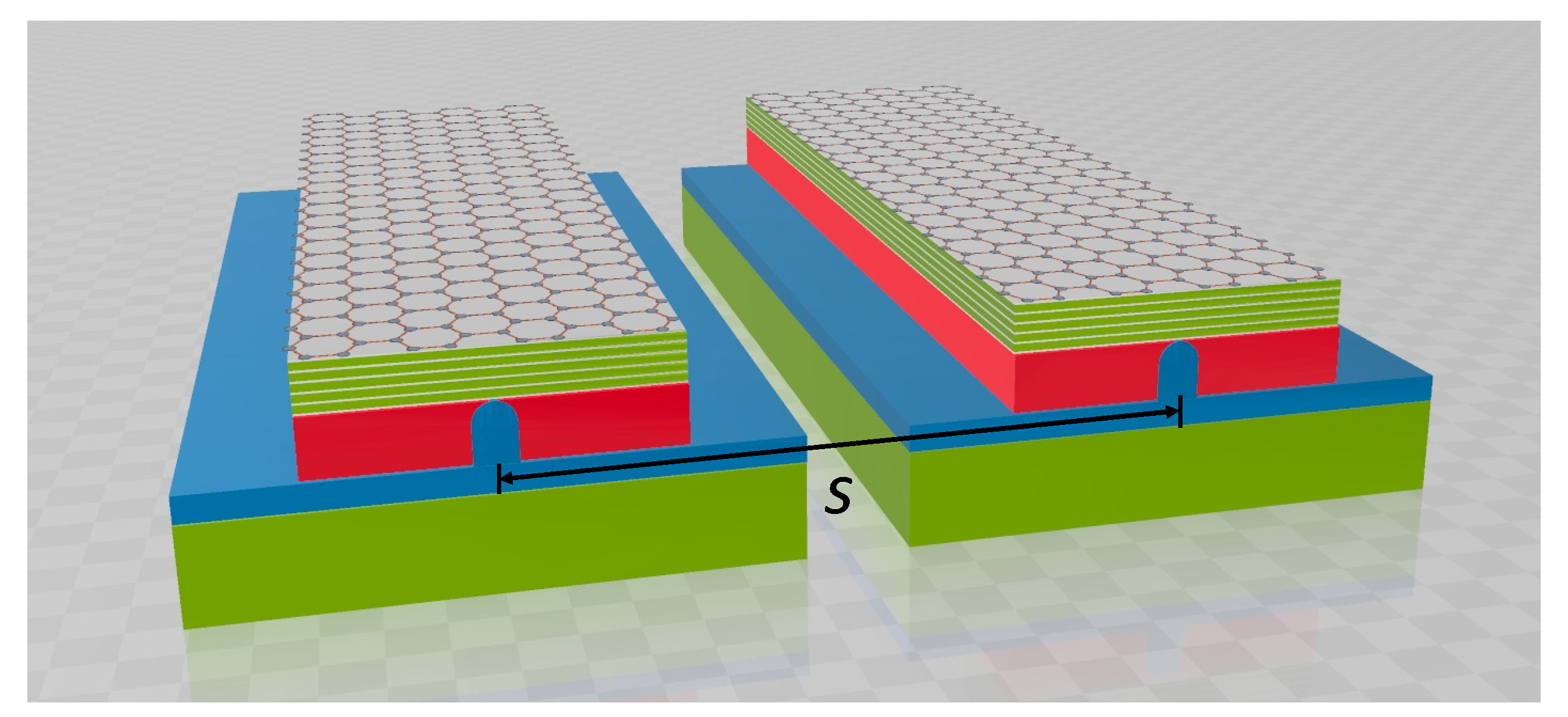
Figure 13.
Schematic of a coupled waveguide consisting of two parallel MLGHPWs with a center-to-center separation s.
Figure 13.
Schematic of a coupled waveguide consisting of two parallel MLGHPWs with a center-to-center separation s.

Figure 14.
Normalized coupling length, Lc/Lave and maximum transfer power, ρmax as functions of separation of waveguides, s for several values of (a) EF at µ = 1 m2/V·s and (b) µ at EF = 0.4 eV for f = 30 THz and the geometry parameters wg = 180 nm, wr = 20 nm, hr = 30 nm, tSi = 25 nm, and td = 25 nm.


Publisher’s Note: MDPI stays neutral with regard to jurisdictional claims in published maps and institutional affiliations. |
© 2021 by the authors. Licensee MDPI, Basel, Switzerland. This article is an open access article distributed under the terms and conditions of the Creative Commons Attribution (CC BY) license (https://creativecommons.org/licenses/by/4.0/).
Share and Cite
MDPI and ACS Style
Huang, C.-C.; Chang, R.-J.; Cheng, C.-W. Ultra-Low-Loss Mid-Infrared Plasmonic Waveguides Based on Multilayer Graphene Metamaterials. Nanomaterials 2021, 11, 2981. https://0-doi-org.brum.beds.ac.uk/10.3390/nano11112981
AMA Style
Huang C-C, Chang R-J, Cheng C-W. Ultra-Low-Loss Mid-Infrared Plasmonic Waveguides Based on Multilayer Graphene Metamaterials. Nanomaterials. 2021; 11(11):2981. https://0-doi-org.brum.beds.ac.uk/10.3390/nano11112981
Chicago/Turabian StyleHuang, Chia-Chien, Ruei-Jan Chang, and Ching-Wen Cheng. 2021. "Ultra-Low-Loss Mid-Infrared Plasmonic Waveguides Based on Multilayer Graphene Metamaterials" Nanomaterials 11, no. 11: 2981. https://0-doi-org.brum.beds.ac.uk/10.3390/nano11112981
Note that from the first issue of 2016, this journal uses article numbers instead of page numbers. See further details here.