
Anisotropic Optical and Vibrational Properties of GeS

 , , , , , and
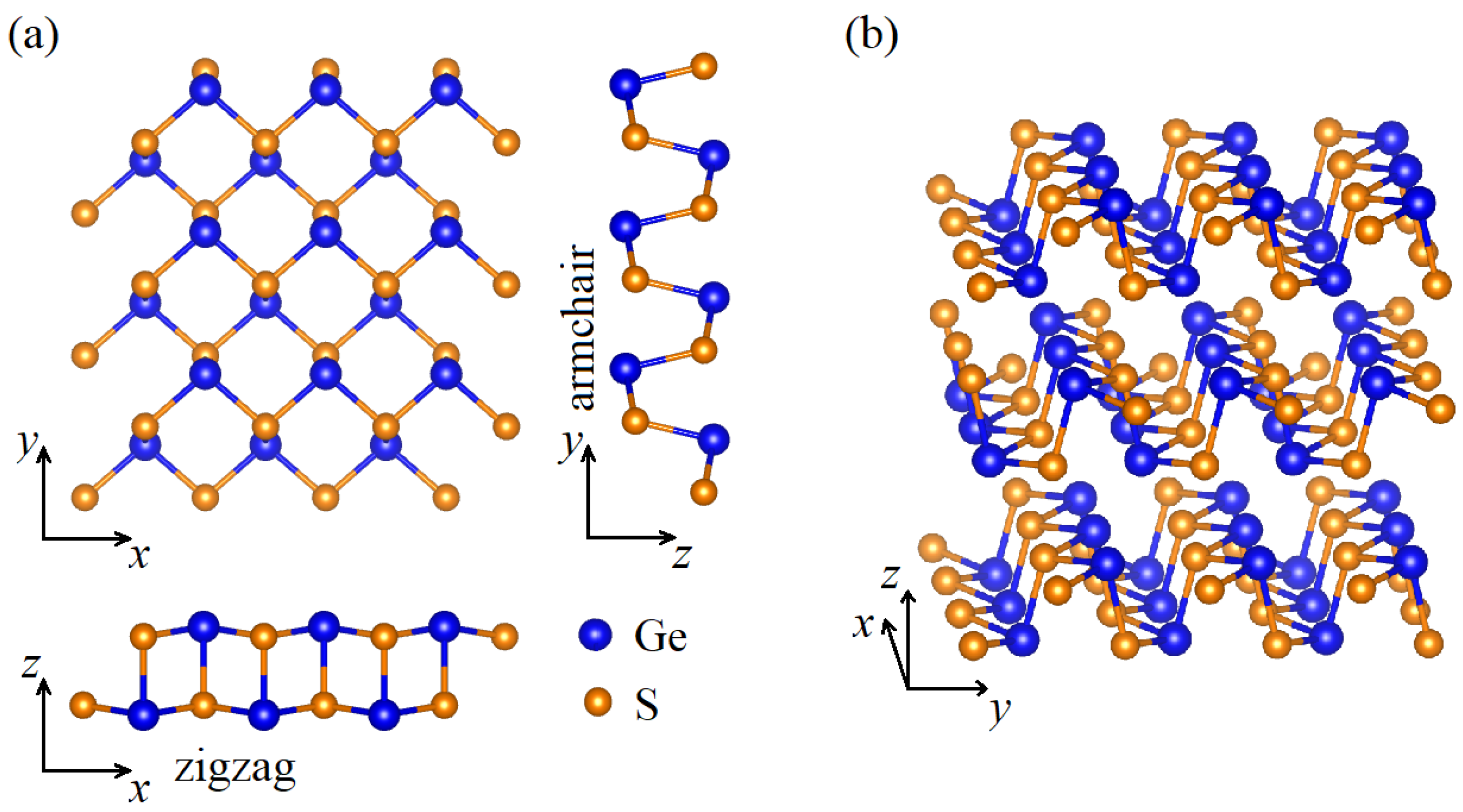
Abstract
:1. Introduction
2. Materials and Methods
2.1. Samples
2.2. Experimental Techniques
2.3. Theoretical Calculations
3. Results
3.1. Crystallographic Structure
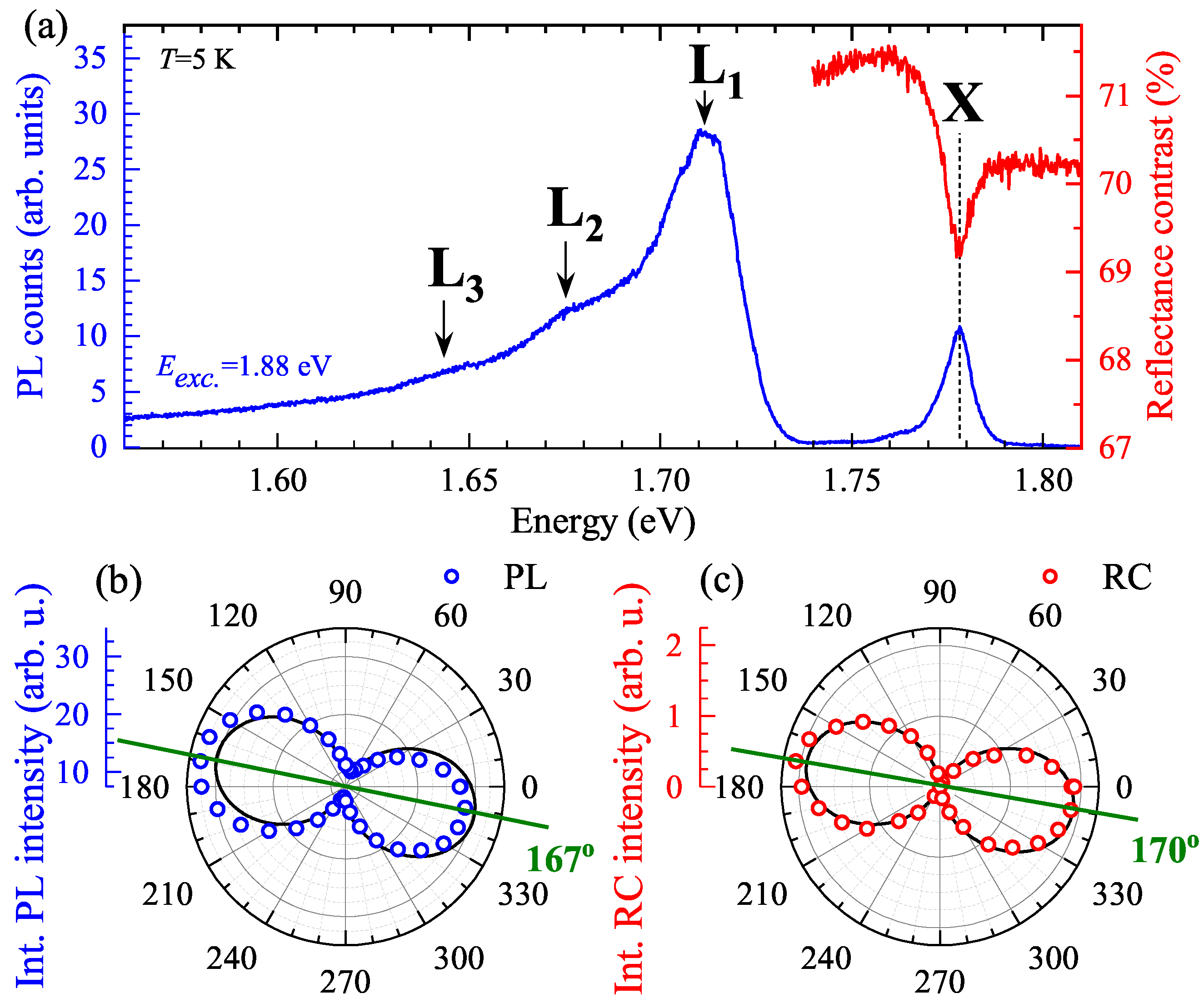
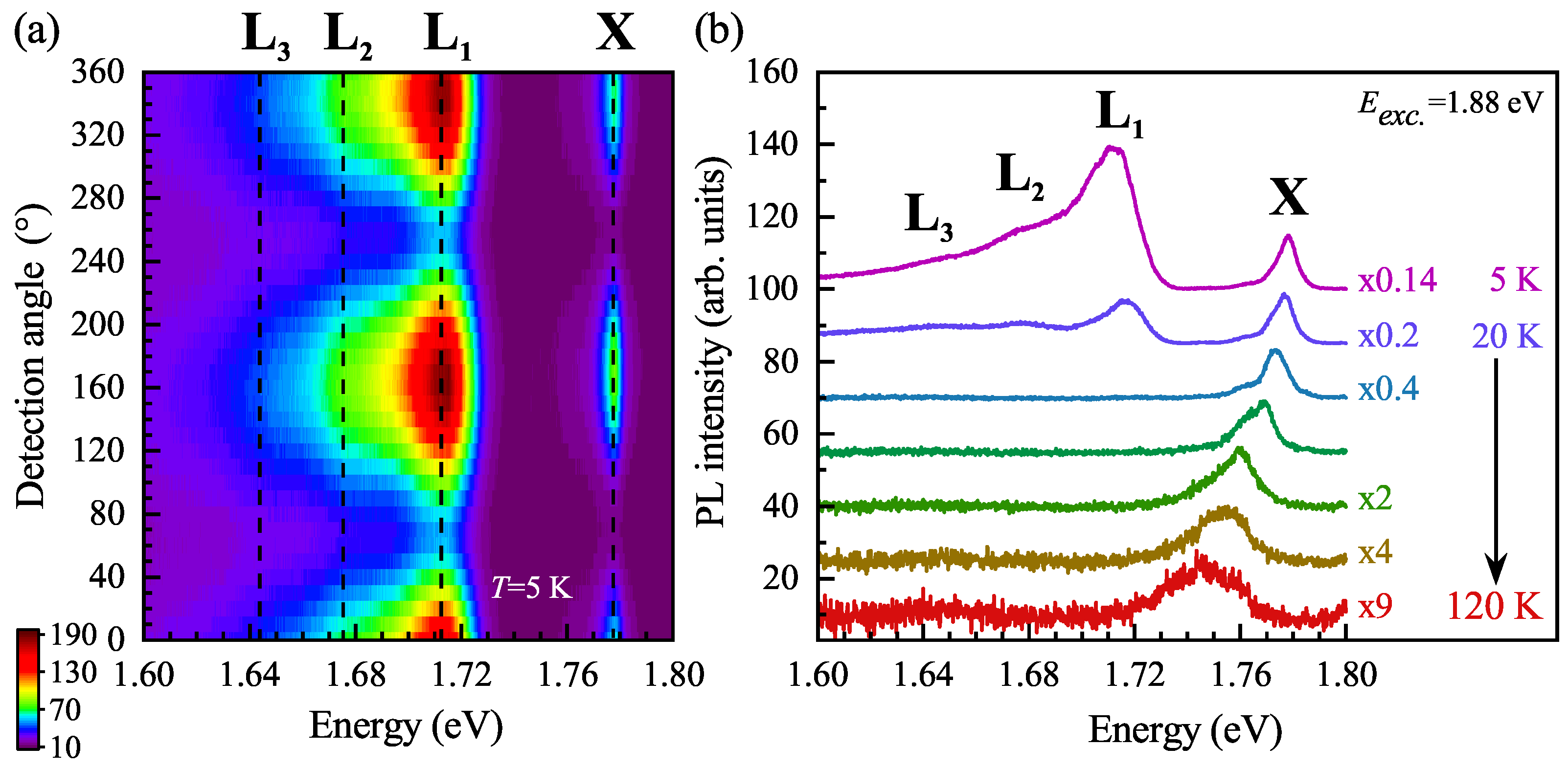
3.2. Optical Properties
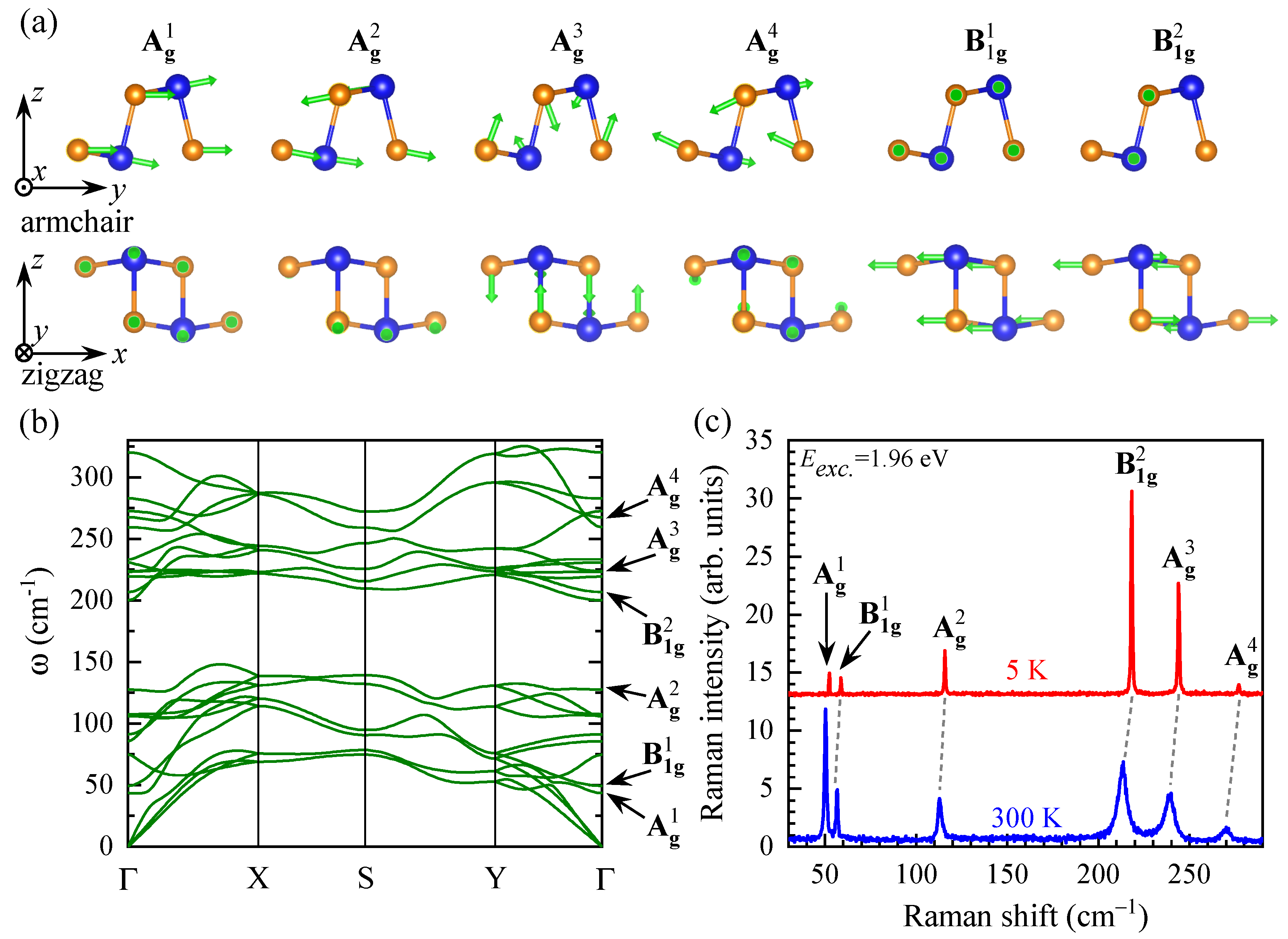
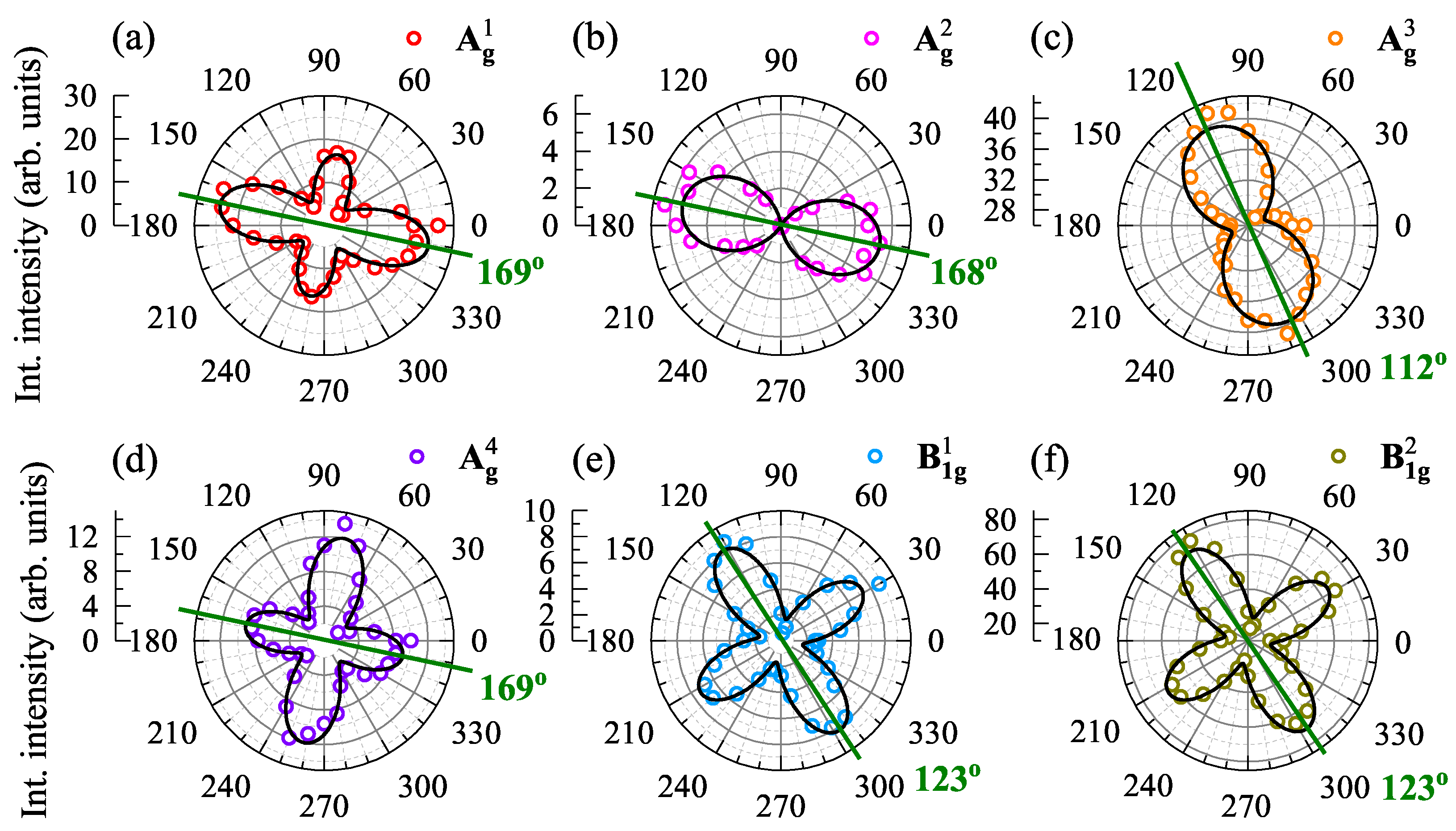
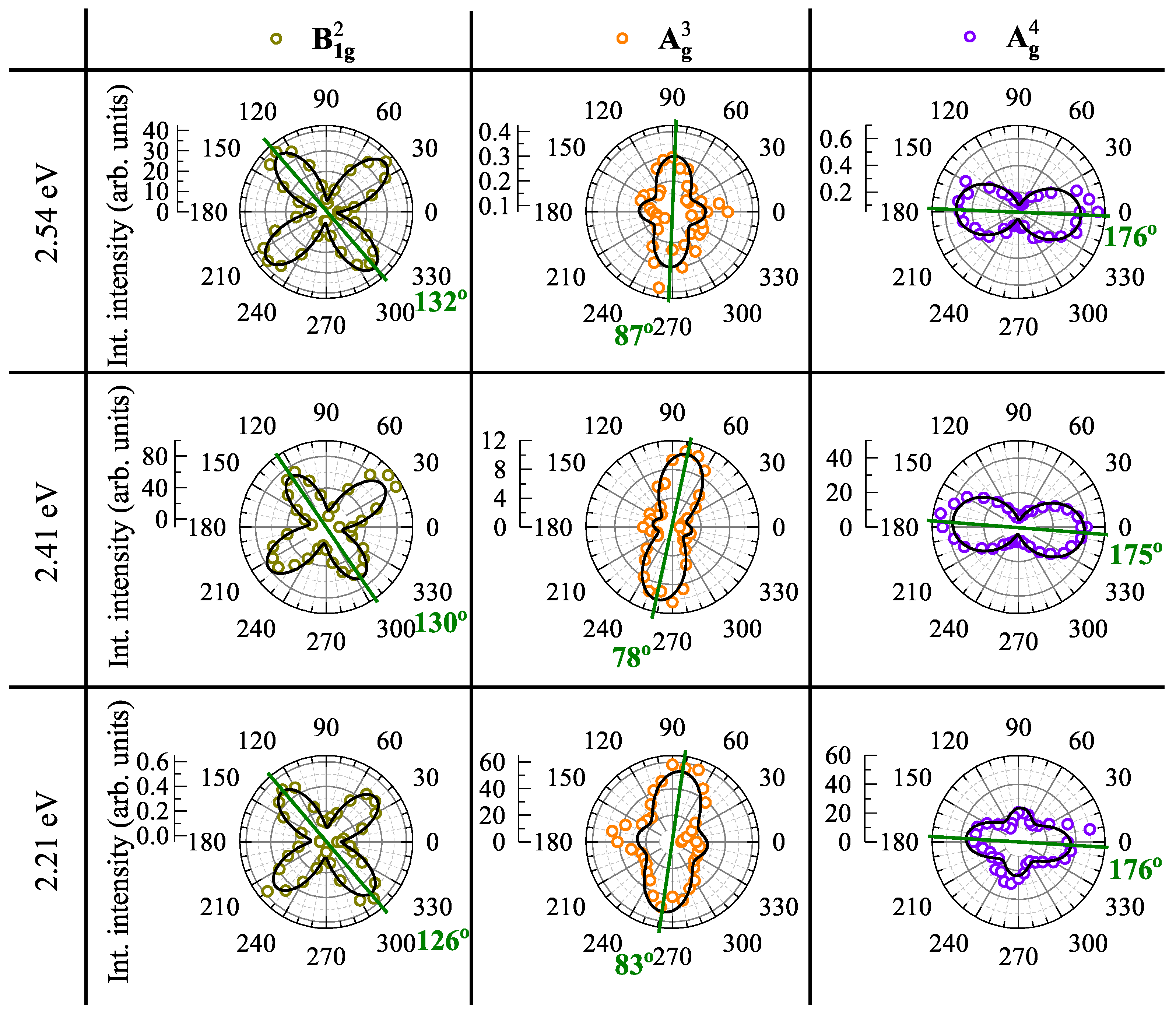
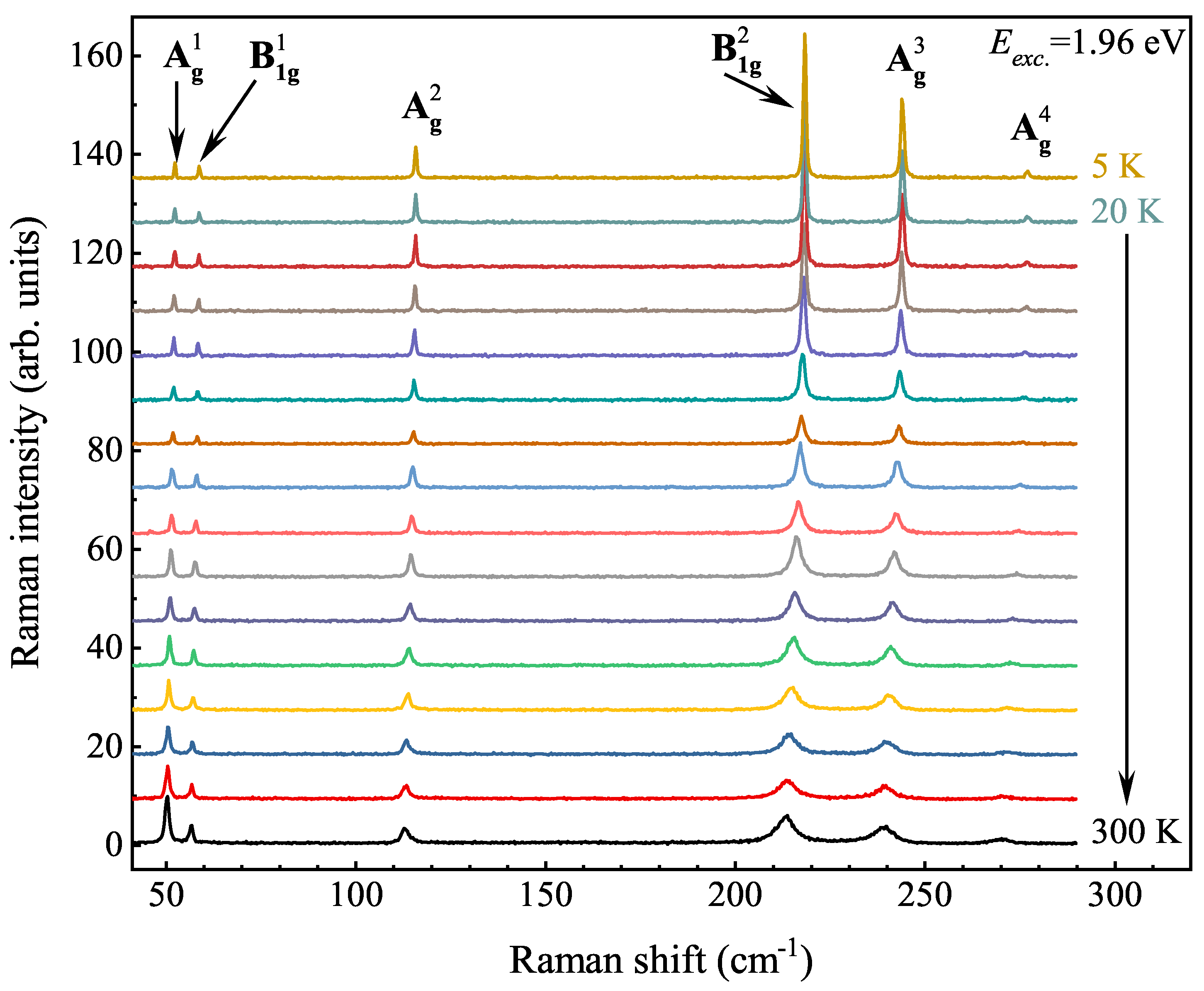
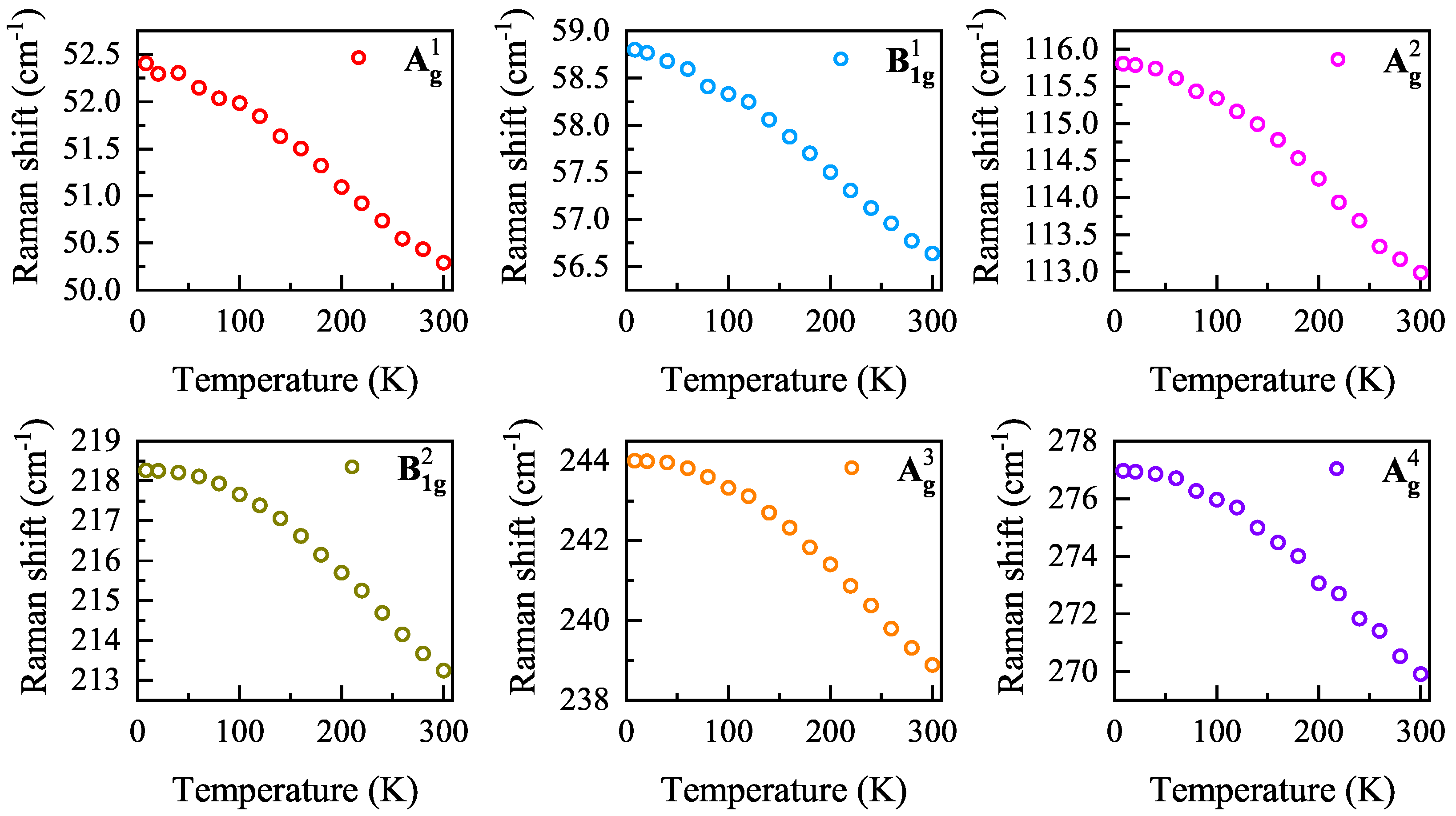
3.3. Vibrational Properties
4. Conclusions
Author Contributions
Funding
Institutional Review Board Statement
Informed Consent Statement
Data Availability Statement
Acknowledgments
Conflicts of Interest
Appendix A. The Temperature Dependence of the Raman Scattering Spectra


References
- Mak, K.F.; Lee, C.; Hone, J.; Shan, J.; Heinz, T.F. Atomically Thin MoS2: A New Direct-Gap Semiconductor. Phys. Rev. Lett. 2010, 105, 136805. [Google Scholar] [CrossRef] [PubMed] [Green Version]
- Arora, A.; Koperski, M.; Nogajewski, K.; Marcus, J.; Faugeras, C.; Potemski, M. Excitonic resonances in thin films of WSe2: From monolayer to bulk material. Nanoscale 2015, 7, 10421. [Google Scholar] [CrossRef] [PubMed] [Green Version]
- Arora, A.; Nogajewski, K.; Molas, M.; Koperski, M.; Potemski, M. Exciton band structure in layered MoSe2: From a monolayer to the bulk limit. Nanoscale 2015, 7, 20769. [Google Scholar] [CrossRef] [PubMed] [Green Version]
- Molas, M.R.; Nogajewski, K.; Slobodeniuk, A.O.; Binder, J.; Bartos, M.; Potemski, M. The optical response of monolayer, few-layer and bulk tungsten disulfide. Nanoscale 2017, 9, 13128. [Google Scholar] [CrossRef] [PubMed] [Green Version]
- Bandurin, D.A.; Tyurnina, A.V.; Yu, G.L.; Mishchenko, A.; Zólyomi, V.; Morozov, S.V.; Kumar, R.K.; Gorbachev, R.V.; Kudrynskyi, Z.R.; Pezzini, S.; et al. High electron mobility, quantum Hall effect and anomalous optical response in atomically thin InSe. Nat. Nanotechnol. 2016, 12, 223–227. [Google Scholar] [CrossRef] [PubMed]
- Ling, X.; Huang, S.; Hasdeo, E.H.; Liang, L.; Parkin, W.M.; Tatsumi, Y.; Nugraha, A.R.T.; Puretzky, A.A.; Das, P.M.; Sumpter, B.G.; et al. Anisotropic Electron-Photon and Electron-Phonon Interactions in Black Phosphorus. Nano Lett. 2016, 16, 2260–2267. [Google Scholar] [CrossRef] [PubMed]
- Ribeiro, H.B.; Pimenta, M.A.; de Matos, C.J.S.; Moreira, R.L.; Rodin, A.S.; Zapata, J.D.; de Souza, E.A.T.; Neto, A.H.C. Unusual Angular Dependence of the Raman Response in Black Phosphorus. ACS Nano 2015, 9, 4270–4276. [Google Scholar] [CrossRef]
- Molas, M.R.; Macewicz, L.; Wieloszyńska, A.; Jakóbczyk, P.; Wysmołek, A.; Bogdanowicz, R.; Jasinski, J.B. Photoluminescence as a probe of phosphorene properties. NPJ 2D Mater. Appl. 2021, 5, 83. [Google Scholar] [CrossRef]
- Choi, Y.; Kim, K.; Lim, S.Y.; Kim, J.; Park, J.M.; Kim, J.H.; Lee, Z.; Cheong, H. Complete determination of the crystallographic orientation of ReX2 (X = S, Se) by polarized Raman spectroscopy. Nanoscale Horiz. 2020, 5, 308–315. [Google Scholar] [CrossRef] [Green Version]
- Kipczak, L.; Grzeszczyk, M.; Olkowska-Pucko, K.; Babiński, A.; Molas, M.R. The optical signature of few-layer ReSe2. J. Appl. Phys. 2020, 128, 044302. [Google Scholar] [CrossRef]
- Li, F.; Liu, X.; Wang, Y.; Li, Y. Anisotropic Electron-Photon and Electron-Phonon Interactions in Black Phosphorus. J. Mater. Chem. C 2016, 4, 2155–2159. [Google Scholar] [CrossRef]
- Ho, C.H.; Li, J.X. Polarized Band-Edge Emission and Dichroic Optical Behavior in Thin Multilayer GeS. Mater. Views 2016, 5, 1600814. [Google Scholar] [CrossRef]
- Tan, D.; Lim, H.E.; Wang, F.; Mohamed, N.B.; Moun, S.; Zhang, W.; Miyauchu, Y.; Ohfuchi, M.; Matsuda, K. Anisotropic optical and electronic properties of two-dimensional layered germanium sulfide. Nano Res. 2017, 2, 546–555. [Google Scholar] [CrossRef]
- Lam, D.; Chen, K.S.; Kang, J.; Liu, X.; Hersam, M.C. Anhydrous Liquid-Phase Exfoliation of Pristine Electrochemically Active GeS Nanosheets. Chem. Mater. 2018, 30, 2245–2250. [Google Scholar] [CrossRef]
- Ribeiro, H.B.; Ramos, S.L.L.M.; Seixas, L.; de Matos, C.J.S.; Pimenta, M.A. Edge phonons in layered orthorhombic GeS and GeSe monochalcogenides. Phys. Rev. B 2019, 100, 094301. [Google Scholar] [CrossRef]
- Oliva, R.; Woźniak, T.; Dybala, F.; Tołłoczko, A.; Kopaczek, J.; Scharoch, P.; Kudrawiec, R. Valley polarization investigation of GeS under high pressure. Phys. Rev. B 2020, 101, 235205. [Google Scholar] [CrossRef]
- Tołłoczko, A.; Oliva, R.; Wożniak, T.; Kopaczek, J.; Scharoch, P.; Kudrawiec, R. Anisotropic optical properties of GeS investigated by optical absorption and photoreflectance. Mater. Adv. 2020, 1, 1886–1894. [Google Scholar] [CrossRef]
- Castellanos-Gomez, A.; Buscema, M.; Molenaar, R.; Singh, V.; Janssen, L.; van der Zant, H.S.J.; Steele, G.A. Deterministic transfer of two-dimensional materials by all-dry viscoelastic stamping. 2D Mater. 2014, 1, 011002. [Google Scholar] [CrossRef]
- Kresse, G.; Furthmüller, J. Efficient iterative schemes for ab initio total-energy calculations using a plane-wave basis set. Phys. Rev. B 1996, 54, 11169–11186. [Google Scholar] [CrossRef]
- Kresse, G.; Joubert, D. From ultrasoft pseudopotentials to the projector augmented-wave method. Phys. Rev. B 1999, 59, 1758–1775. [Google Scholar] [CrossRef]
- Perdew, J.P.; Burke, K.; Ernzerhof, M. Generalized Gradient Approximation Made Simple. Phys. Rev. Lett. 1996, 77, 3865–3868. [Google Scholar] [CrossRef] [PubMed] [Green Version]
- Grimme, S.; Antony, J.; Ehrlich, S.; Krieg, H. A consistent and accurate ab initio parametrization of density functional dispersion correction (DFT-D) for the 94 elements H-Pu. J. Chem. Phys. 2010, 132, 154104. [Google Scholar] [CrossRef] [PubMed] [Green Version]
- Parlinski, K.; Li, Z.Q.; Kawazoe, Y. First-Principles Determination of the Soft Mode in Cubic ZrO2. Phys. Rev. Lett. 1997, 78, 4063–4066. [Google Scholar] [CrossRef]
- Togo, A.; Tanaka, I. First principles phonon calculations in materials science. Scr. Mater. 2015, 108, 1–5. [Google Scholar] [CrossRef] [Green Version]
- Togo, A.; Tanaka, I. Spglib: A software library for crystal symmetry search. arXiv 2018, arXiv:1808.01590. [Google Scholar]
- Wiedemeier, H.; Siemers, P.A. The Thermal Expansion of GeS and GeTe. Z. Anorg. Allg. Chem. 1977, 431, 299–304. [Google Scholar] [CrossRef]
- Hecht, E. OPTics, 5th ed.; Pearson Education Limited: Harlow, UK, 2017; p. 347. [Google Scholar]
- Plechinger, G.; Nagler, P.; Kraus, J.; Paradiso, N.; Strunk, C.; Schüller, C.; Korn, T. Identification of excitons, trions and biexcitons in single-layer WS2. Phys. Status Solidi RRL—Rapid Res. Lett. 2015, 9, 457–461. [Google Scholar] [CrossRef] [Green Version]
- Shang, J.; Shen, X.; Cong, C.; Peimyoo, N.; Cao, B.; Eginligil, M.; Yu, T. Observation of Excitonic Fine Structure in a 2D Transition-Metal Dichalcogenide Semiconductor. ACS Nano 2015, 9, 647–655. [Google Scholar] [CrossRef]
- Plechinger, G.; Nagler, P.; Arora, A.; Granados del Águila, A.; Ballottin, M.V.; Frank, T.; Steinleitner, P.; Gmitra, M.; Fabian, J.; Christianen, P.C.M.; et al. Excitonic Valley Effects in Monolayer WS2 under High Magnetic Fields. Nano Lett. 2016, 16, 7899–7904. [Google Scholar] [CrossRef] [Green Version]
- Kłopotowski, Ł.; Backes, C.; Mitioglu, A.A.; Vega-Mayoral, V.; Hanlon, D.; Coleman, J.N.; Ivanov, V.Y.; Maude, D.K.; Plochocka, P. Revealing the nature of excitons in liquid exfoliated monolayer tungsten disulphide. Nanotechnology 2016, 27, 425701. [Google Scholar] [CrossRef] [Green Version]
- Zou, B.; Wei, Y.; Zhou, Y.; Ke, D.; Zhang, X.; Zhang, M.; Yip, C.T.; Chen, X.; Li, W.; Sun, H. Unambiguous determination of crystal orientation in black phosphorus by angle-resolved polarized Raman spectroscopy. Nanoscale Horiz. 2021, 6, 809–818. [Google Scholar] [CrossRef] [PubMed]
- Kim, J.; Lee, J.U.; Lee, J.; Park, H.J.; Lee, Z.; Lee, C.; Cheong, H. Anomalous polarization dependence of Raman scattering and crystallographic orientation of black phosphorus. Nanoscale 2015, 7, 18708–18715. [Google Scholar] [CrossRef] [PubMed] [Green Version]
- Sriv, T.; Nguyen, T.M.H.; Lee, Y.; Lim, S.Y.; Nguyen, V.Q.; Kim, K.; Cho, S.; Cheong, H. Optical phonons of SnSe(1-x)Sx layered semiconductor alloys. Sci. Rep. 2020, 10, 11761. [Google Scholar] [CrossRef] [PubMed]


Publisher’s Note: MDPI stays neutral with regard to jurisdictional claims in published maps and institutional affiliations. |
© 2021 by the authors. Licensee MDPI, Basel, Switzerland. This article is an open access article distributed under the terms and conditions of the Creative Commons Attribution (CC BY) license (https://creativecommons.org/licenses/by/4.0/).
Share and Cite
Zawadzka, N.; Kipczak, Ł.; Woźniak, T.; Olkowska-Pucko, K.; Grzeszczyk, M.; Babiński, A.; Molas, M.R. Anisotropic Optical and Vibrational Properties of GeS. Nanomaterials 2021, 11, 3109. https://0-doi-org.brum.beds.ac.uk/10.3390/nano11113109
Zawadzka N, Kipczak Ł, Woźniak T, Olkowska-Pucko K, Grzeszczyk M, Babiński A, Molas MR. Anisotropic Optical and Vibrational Properties of GeS. Nanomaterials. 2021; 11(11):3109. https://0-doi-org.brum.beds.ac.uk/10.3390/nano11113109
Chicago/Turabian StyleZawadzka, Natalia, Łucja Kipczak, Tomasz Woźniak, Katarzyna Olkowska-Pucko, Magdalena Grzeszczyk, Adam Babiński, and Maciej R. Molas. 2021. "Anisotropic Optical and Vibrational Properties of GeS" Nanomaterials 11, no. 11: 3109. https://0-doi-org.brum.beds.ac.uk/10.3390/nano11113109