Article

Ultrahigh Sensitivity of a Plasmonic Pressure Sensor with a Compact Size

by
Chung-Ting Chou Chao
1,
Yuan-Fong Chou Chau
2,*,
Sy-Hann Chen
3,
Hung Ji Huang
4,
Chee Ming Lim
2,
Muhammad Raziq Rahimi Kooh
2,
Roshan Thotagamuge
2 and
Hai-Pang Chiang
1,*
1
Department of Optoelectronics and Materials Technology, National Taiwan Ocean University, Keelung 20224, Taiwan
2
Centre for Advanced Material and Energy Sciences, Universiti Brunei Darussalam, Tungku Link, Gadong, Bandar Seri Begawan BE1410, Brunei
3
Department of Electrophysics, National Chiayi University, Chiayi 600, Taiwan
4
National Applied Research Laboratories, Taiwan Instrument Research Institute, Hsinchu 300, Taiwan
*
Authors to whom correspondence should be addressed.
Nanomaterials 2021, 11(11), 3147; https://0-doi-org.brum.beds.ac.uk/10.3390/nano11113147
Submission received: 20 October 2021 / Revised: 18 November 2021 / Accepted: 19 November 2021 / Published: 21 November 2021

Abstract

:
This study proposes a compact plasmonic metal-insulator-metal pressure sensor comprising a bus waveguide and a resonator, including one horizontal slot and several stubs. We calculate the transmittance spectrum and the electromagnetic field distribution using the finite element method. When the resonator’s top layer undergoes pressure, the resonance wavelength redshifts with increasing deformation, and their relation is nearly linear. The designed pressure sensor possesses the merits of ultrahigh sensitivity, multiple modes, and a simple structure. The maximum sensitivity and resonance wavelength shift can achieve 592.44 nm/MPa and 364 nm, respectively, which are the highest values to our knowledge. The obtained sensitivity shows 23.32 times compared to the highest one reported in the literature. The modeled design paves a promising path for applications in the nanophotonic field.

1. Introduction

Recently, surface plasmon polaritons (SPPs) are electromagnetic (EM) waves traveling along the dielectric-metal border and forming collective oscillations of electrons and photons at resonant wavelengths [1,2,3,4,5,6,7,8,9]. SPPs can facilitate light–matter interaction between dielectric medium and metal nanoparticles (MNPs) since they can configure light into the nanometer domain and overcome the diffraction limit [10,11,12,13,14,15]. SPPs based on metal-insulator-metal (MIM) bus waveguide (WG) combined with single or several nanocavities (or resonators) has a myriad of considerations due to its unique optical properties, including low losses, long propagation distance, easy fabrication, and compatible integrated optical circuits (IOCs) [16,17,18,19,20]. Plasmonic MIM WGs combined with resonators have many applications in nanophotonics fields [21,22,23], such as optical switches [24], beam splitters [25,26], perfect absorbers [27,28,29], optical filters [30,31,32], and plasmonic sensor [33,34,35] because of their robust light localization and confinement and light tunability at a subwavelength regime and excellent performance of sensitivity to the variation of ambient materials.
A MIM-based plasmonic pressure sensor is an optical element that can undergo exerted pressure and transform it into electrical or optical signals [19,36,37,38]. Plasmonic optical pressure sensors with the immune of EM wave disturbance have received considerable attention ever since numerous applications in the engineering field of biomedicines, mechanics, and electric optics [39]. Most reported optical pressure sensors are based on the Fabry–Perot interferometer [40,41], SiO2 diaphragm [42], monolithic capacitive pressure sensor [43], Mach–Zehnder interferometer [44], optical fibers [45,46], etc. They show a larger size and have a drawback of less compatibility to IOCs.
The absorption peaks of surface plasmon resonance (SPR) in gold nanospheres (AuNSs) and gold nanorods (Au NRs) are highly sensitive to their surrounding medium and to their refractive index changes. Martín-Sánchez et al. have found that the plasmonic properties of AuNSs can be used as the basis for sensing changes in the surrounding medium under very high pressure ranging from 0 to −60 GPa [47]. Runowski et al. reported that Au nanorods (NRs) could effectively detect phase transitions of compressed compounds, whether liquid and solid, by measuring their refractive index. They observed its subtle refractive index changes and the properties of high-pressure phases by using high-pressure absorption Vis-NIR spectroscopy [48].
In order to be compatible with IOCs, the strategy to miniaturize the pressure sensor’s size is crucial. Recently, many research groups proposed various optical pressure sensors to satisfy the compatibility of IOCs. Chaudhary et al. presented a hydrostatic pressure sensor using photonic crystal fibers (PCFs) with a sensitivity of 0.0116 nm/MPa [49]. Dinodiya et al. developed a photonic crystal’s pressure sensor based on Si and GaAs and claimed that the obtained sensitivity could reach 17.00 nm/GPa [50]. Another approach based on a nanostructure grating can detect pressure ganging in 0–1 kPa [51]. In ref. [37], Zhao et al. reported a nano-optomechanical pressure sensor employing a ring cavity with a sensitivity of 1.47 pm/kPa. Yao and his collaborators designed a fiber-tip pressure sensor, and the sensitivity can achieve 4.29 nm/MPa [40]. Wu et al. also illustrated a pressure sensor employing an H-type SPP resonator and found the measurable minimum pressure to be about 2.6 × 10⁴ Pa [52]. Yu et al. studied flexible plasmonic pressure sensors based on layered two-dimensional (2-D) heterostructures and reported the highest detecting sensitivity of 20.8 k/Pa at the SPR angle [53]. Recently, Tathfif et al. proposed a high sensitivity pressure sensor of 25.4 nm/MPa using thirty-four silver (Ag) nanorods embedded in the slot and bus WG and claimed that the obtained sensitivity is the highest one compared to the previous literature [54]. However, their designed structure has the drawback of complex fabrication because they place thirty-four Ag nanorods in bus WGs and resonators. Moreover, the sensitivity must further improve as high as possible in order to meet the current pressure sensing application requirements.
This paper designs a compact plasmonic pressure sensor composed of a MIM bus WG and a resonator, including a horizontal slot and several stubs. The resonator’s size of the designed sensor is as small as a few hundred nanometers. We employed the finite element method (FEM) to investigate the plasmonic pressure sensor’s transmittance features and EM wave distribution and calculated the relation between resonator deformation and sensitivity. Simulation results demonstrate that the resonance wavelength has a redshift when the resonator deforms. Thus, the resonator’s deformation can measure the sensitivity of the plasmonic pressure sensor.
Furthermore, the deformation is linearly proportional to the wavelength shift in a broad wavelength range. As a result, the designed pressure sensor has an ultra-high sensitivity of 592.44 nm/MPa, the highest value reported to date, and demonstrates 23.32 times the sensitivity compared to the highest one (i.e., ref. [54]) published before this study. Moreover, the designed structure is straightforward and is rarely investigated before. Due to high sensitivity and compactness, the proposed plasmonic pressure sensor is a pivotal candidate for different on-chip sensing purposes and offers a chance for designing a beneficial nanophotonic device.

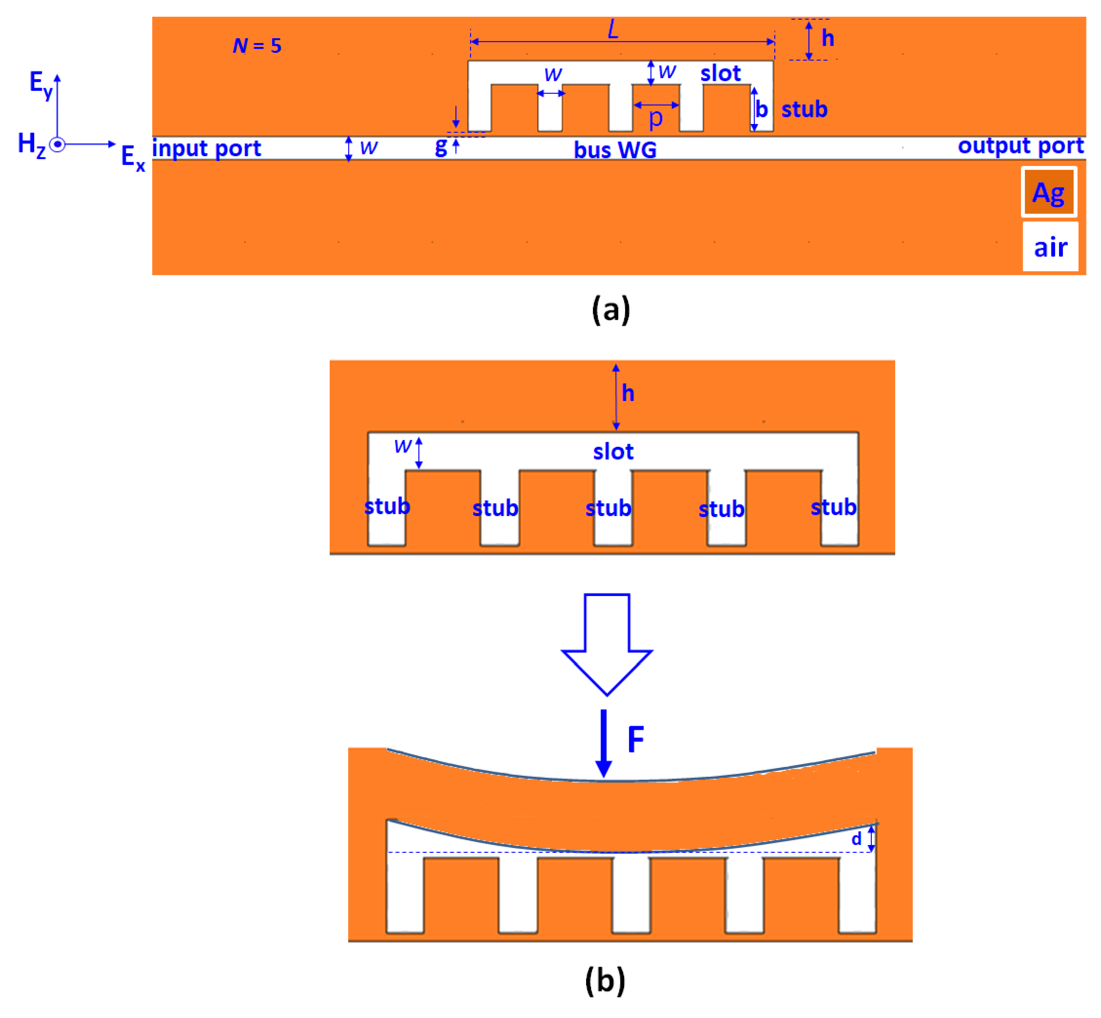
2. Simulation Models, Analysis Method, and Fundamentals

Figure 1a,b illustrate the schematic diagrams of the designed sensor, i.e., a MIM bus WG (width w) side-coupled to a resonator which contains one horizontal slot (width w and length L) and five vertical stubs (width w, height b, and gap distance between two stubs P), respectively. The thickness of the Ag layer above the horizontal slot is h, and the gap distance between the bus WG and the resonator is g. In Figure 1, the golden and white parts stand for Ag and air. If an applied pressure F is exerted on the top of the Ag layer, it will bend downwards with deformation of d (see Figure 1b), which is stated according to [37,52,54,55].
A TM-polarized incident light couples with the fundamental SPP mode [56,57,58] into the bus WG’s input port, and the transmission power reaches the output port [59,60]. The popular plasmonic metals are gold (Au) and Ag [61,62]. Ag is used in this study due to the cost consumption that must be considered for the future fabrication. Moreover, the EM wave response of Ag has the smallest imaginary part of relative permittivity within the near-infrared level. As a result, its power consumption is low compared to other metals (e.g., Au, copper, or platinum). The Drude model can characterize the permittivity (εm) of Ag [63]. A 2-D physical model replaces the 3-D physical model because the structure height in the z-axis is much larger than the skin depth of SPPs in the x-axes and y-axes. FEM-based COMSOL Multiphysics with ultrafine mesh sizes was used to simulate the transmittance spectrum and EM wave distributions. Perfectly matched layers were used to absorb the outgoing waves without reflection. The SPPs’ mode can be generated in the plasmonic system when the incident light approaches the intrinsic resonance wavelength (λres). If Δφ = 2πm (m = 1,2,3 …), λres can be described as follows [64,65].
λ res = 2 L e f f R e ( n eff ) m ϕ 2 π  
Here, Leff represents the resonator’s effective length, φ and Re(neff) are the phase shift and the real part of the effective refractive index, respectively, and neff is defined as follows:
R e ( n eff ) = ( ε s i l v e r + ( k k 0 ) 2 ) 1 2
where k = 2π/λ is the wave vector, and k0 is the wave vector in the free space.
The transmittance (T) can be calculated by T = Pout (output power)/Pin (input power). FWHM is the full width at half-maximum. Quantifying the ratio of the quality factor and modal volume indicates how sensitive the tailored device is.
High values of the QF/V ratio correspond to significant and robust light–matter interaction [66]. Therefore, the quality factor (QF) and modal volume can be defined as λres/FWHM and QF/V, respectively [67,68,69].
Moreover, we define the dipping strength (ΔD) in Equation (3), i.e., the difference between the transmittance peak (Tpeak) and transmittance dip (Tdip) [70]; see the inset of Figure 2.
ΔD = (Tpeak − Tdip) × 100%
Slater’s law can express the resonant frequency shift (∂f) and the variation in the resonator’s volume (dV) by using the following [71]:
f f = ( ε 0 E 2 μ 0 H 2 ) d V V ( ε 0 E 2 + μ 0 H 2 ) d V
where f is the resonant frequency of resonating area with a volume of V. H and E are magnetic and electric fields [72].
Regarding the top Ag layer as a flat plane (length L and thickness h), the pressure (F, in the unit of Pa) applied on the sensor and deformation (d) can be calculated as follows [52]:
F = 2 Y d h 3 L 4
where F and Y represent the pressure applied on the sensor and Young’s modulus of Ag (Y = 7.5 × 10¹⁰ Pa), respectively. Wavelength shift (Δλ) is associated with the resonator’s deformation (d) with a coefficient of η. Therefore, Equation (5) can be modified as follows.
F = 2 Y h 3 η L 4 Δ λ
The sensitivity (S) of the pressure sensor can be described by the following [55].
S = Δ λ Δ F = L 4 Δ λ 2 Y h 3 Δ d
Measurement of transmission loss (TL) is a unit of decibel (dB), and it can utilize the following formula.
T L = 10   l o g 10 P i n P o u t   ( dB )
Pin is the power of incident wave coming towards a defined area (i.e., the designed structure), and Pout is the power of the wave transmitted away from the designed system.
Since the advance in nanofabrication, the fabrication of the designed pressure sensor is achievable with current manufacturing technologies [73]. The MIM waveguide with a rectangular shape can be implemented by using stripping and ion beam lithography processes [74]. However, the objective of this paper is not to concentrate on fabrication methods. As an alternative, several potential studies that studied this issue closely is suggested [75,76].

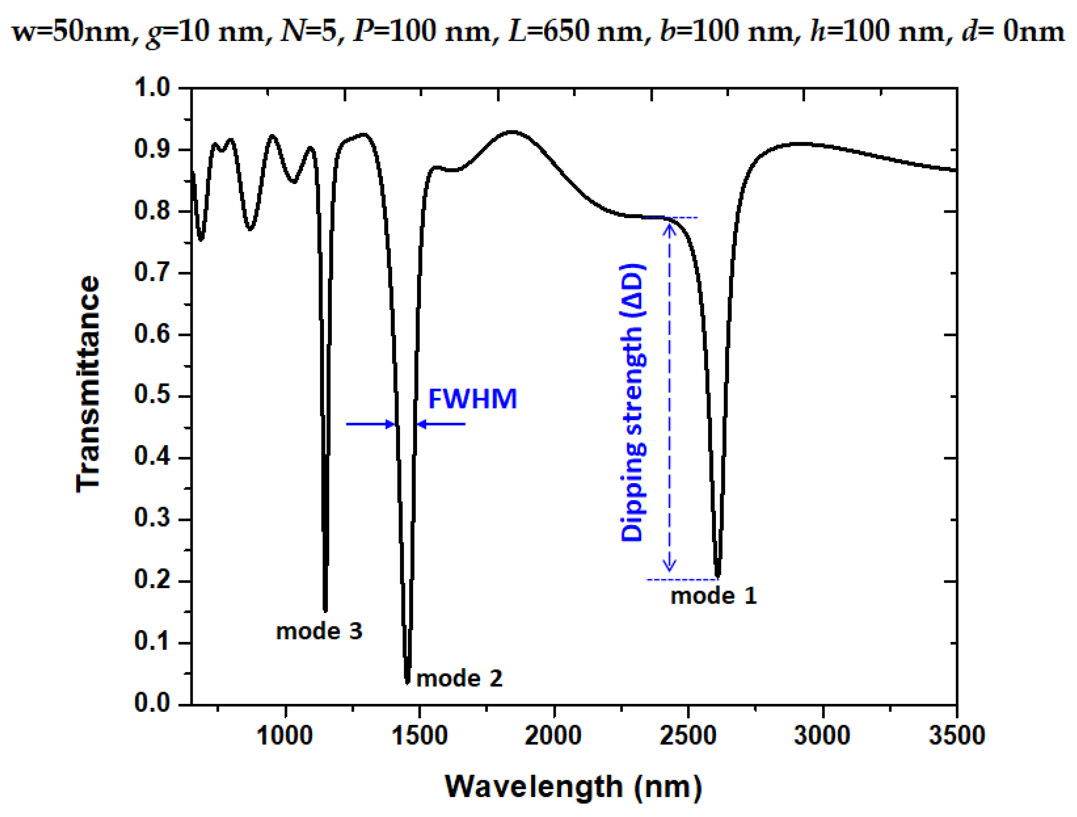
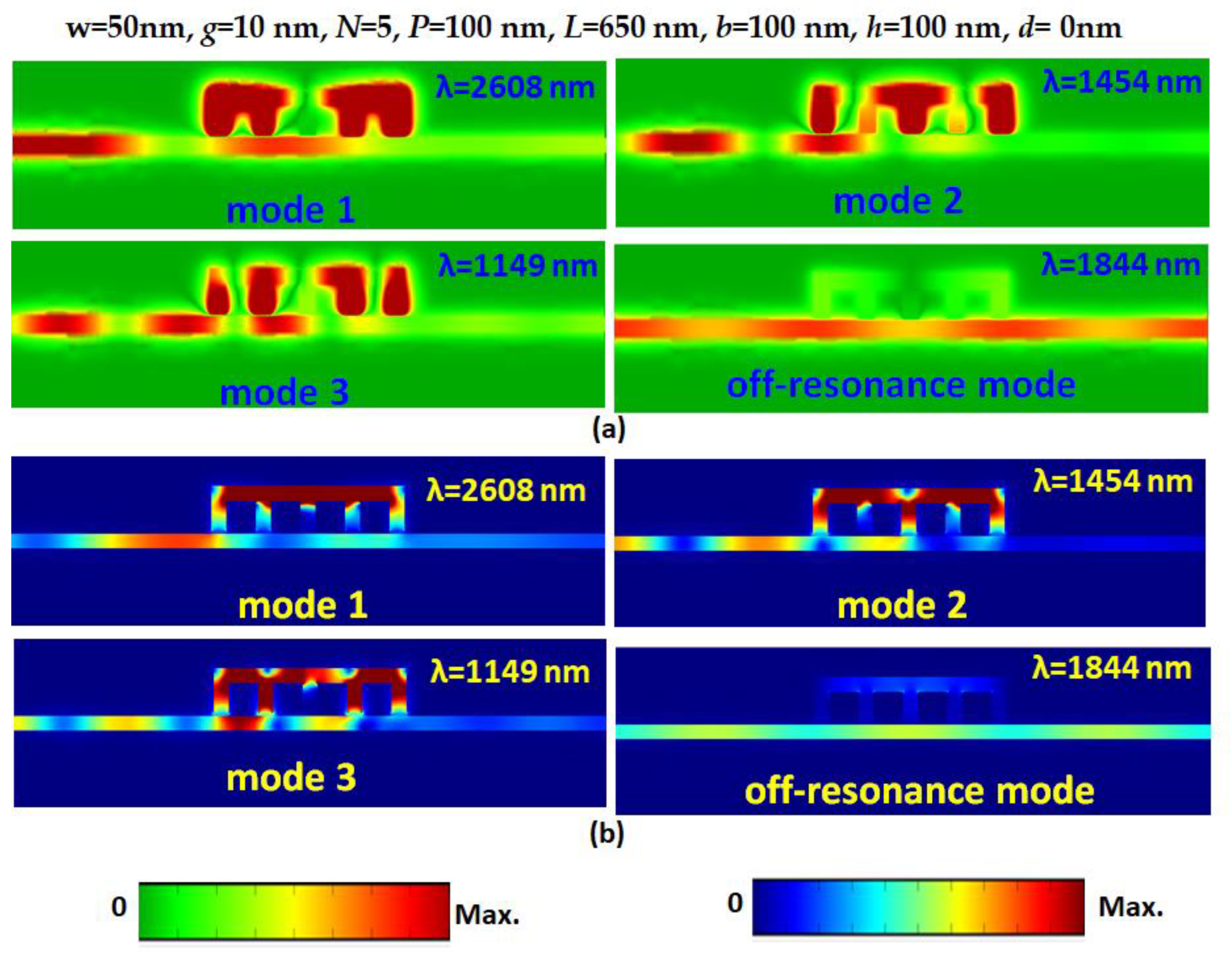
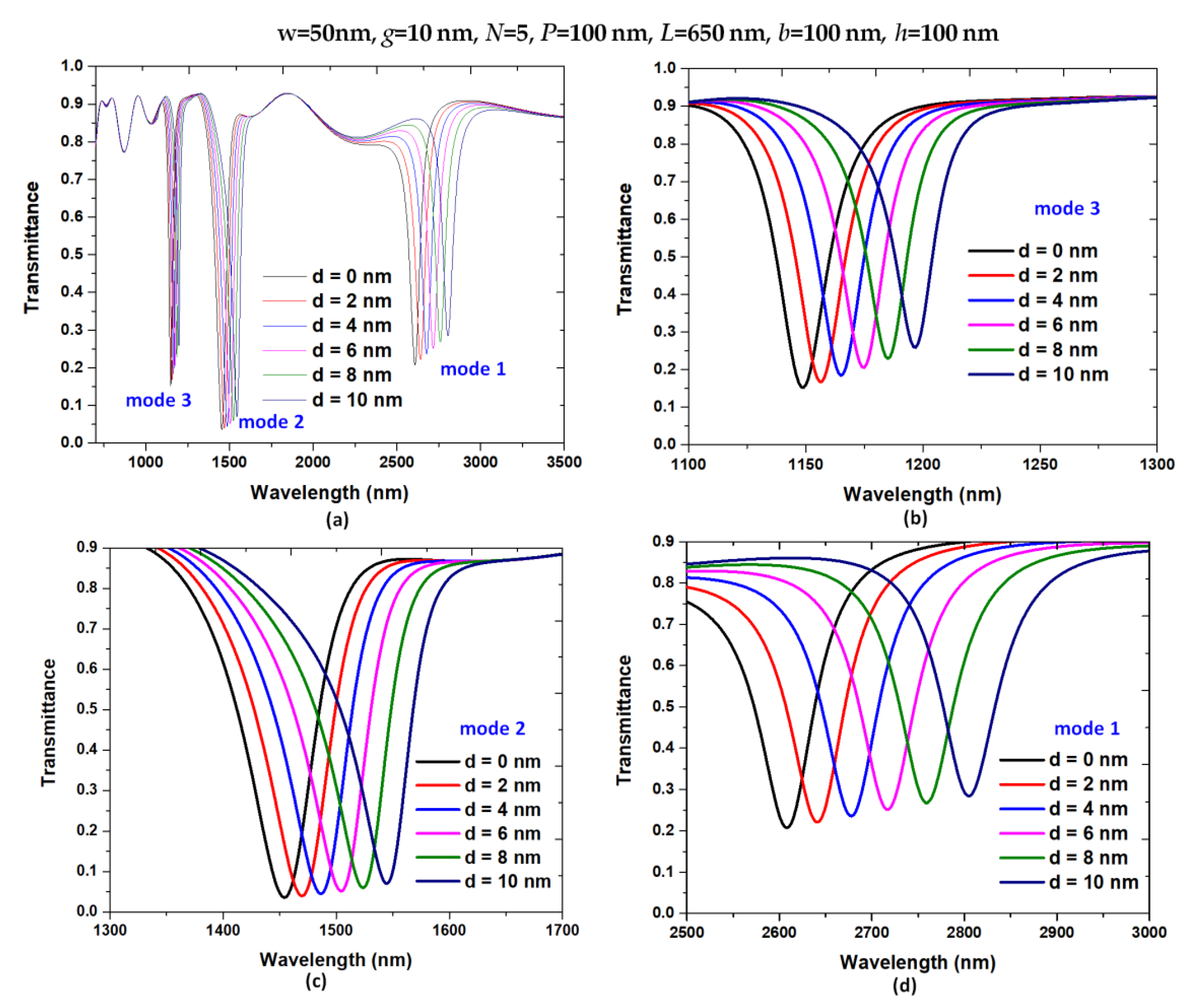
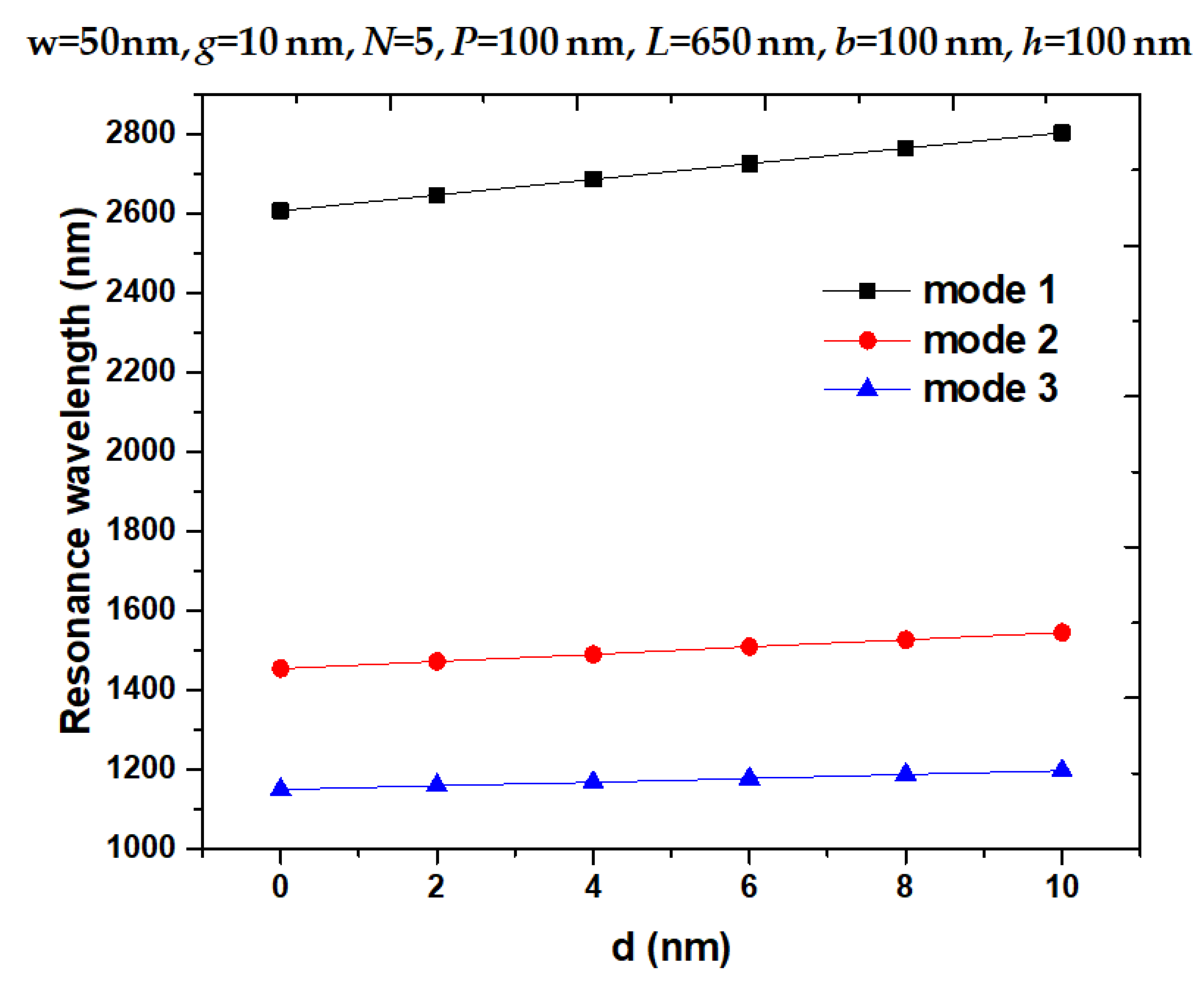
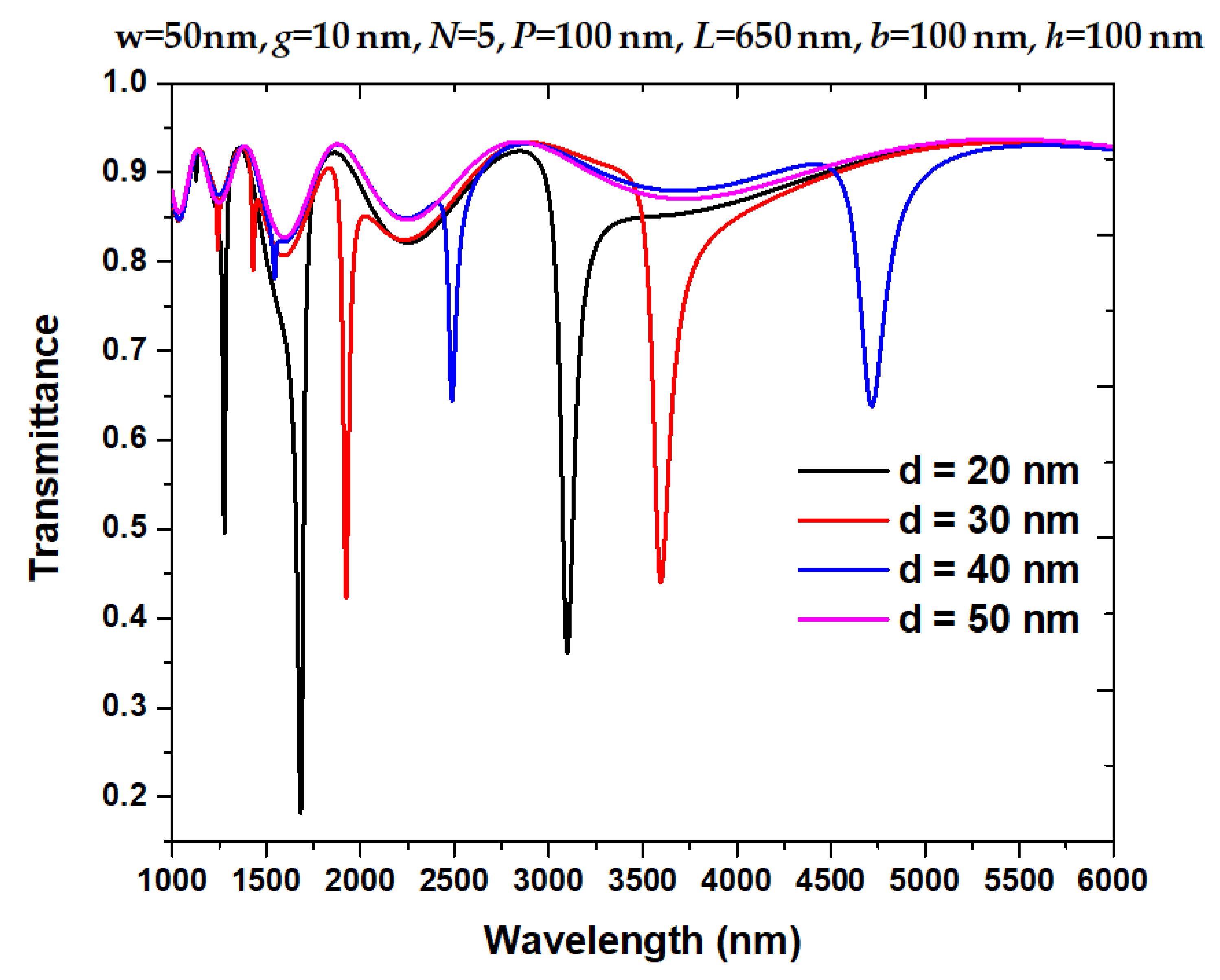
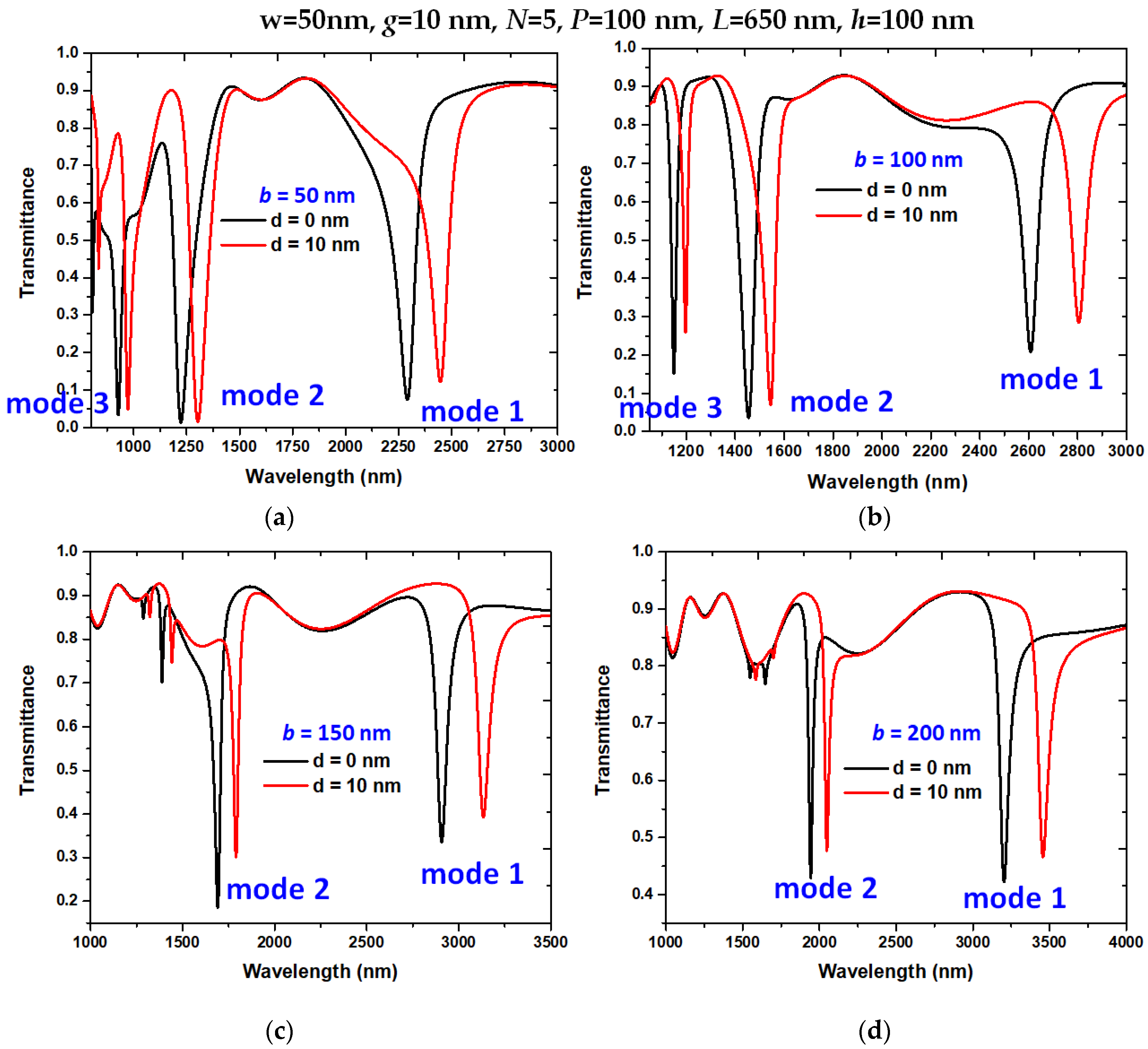
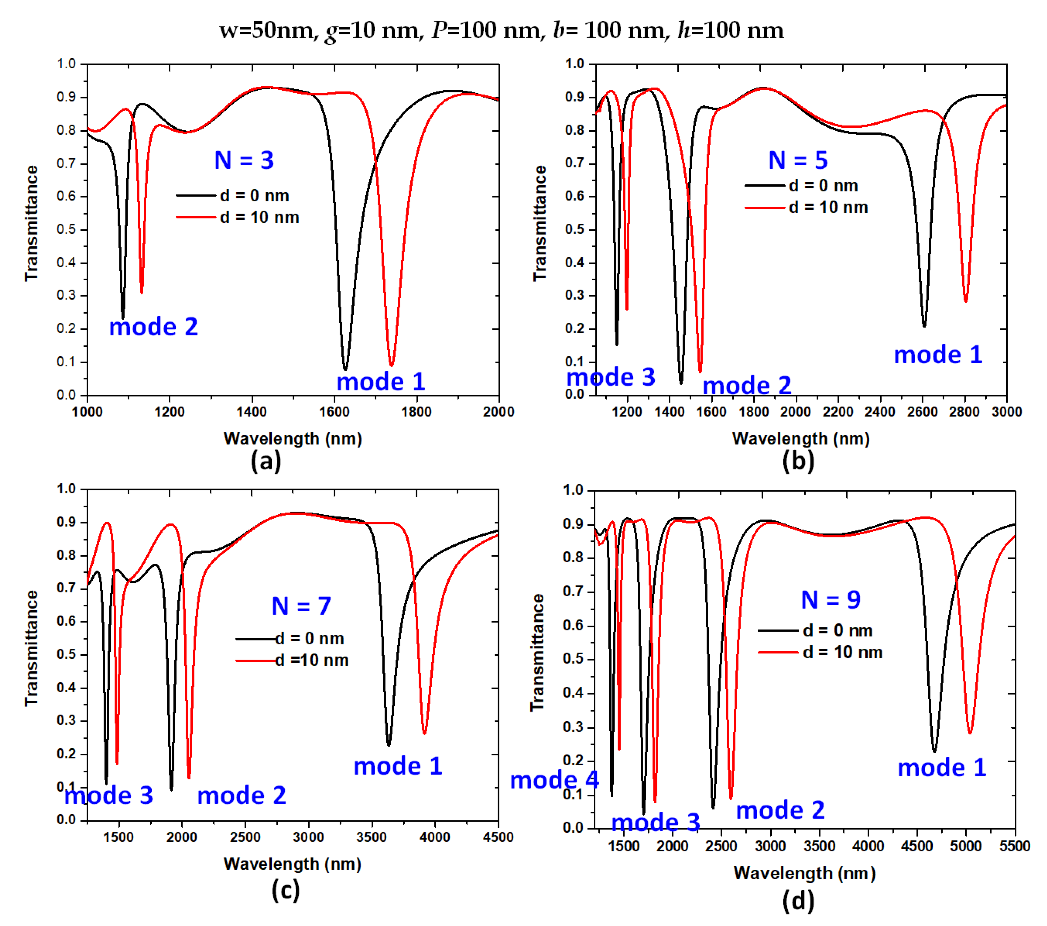
3. Results and Discussion

Figure 2 illustrates the transmittance spectrum for the designed structure at the situation without any pressure on the system (i.e., d = 0 nm). We retain bus WG’s width as w = 50 nm to guarantee that the TM mode can travel in bus WG, horizontal slot and bottom stubs and g = 10 nm was used for obtaining a better coupling effect between bus WG and resonator. The default structural parameters, w, g, P, L, b, h, and d, are 50 nm, 10 nm, 100 nm, 650 nm, 100 nm, and 0 nm, respectively. The resonator size of the designed structure is compact and much smaller than previous designs (e.g., [77,78]). We marked the mode numbers in Figure 2. As observed, three resonance modes correspond to mode 1 and to mode 3, which are attributed to the cavity plasmon resonance (CPR) and SPR modes between bus WG and resonator [10,79]. We compared the resonance wavelength (λres), FWHM, ΔD, and QF of the designed structure at corresponding resonance modes in Table 1. According to Table 1, we found that resonance dips in the developed system have a more profound dipping strength (∆D), a narrower FWHM, and a higher QF than others in the published literature (e.g., [52,54,80]). Moreover, the calculated transmission losses (based on Equation (8)) are 8.34 dB, 11.61 dB and 9.13 dB, respectively. According to the simulations (not shown here for the sake of simplicity), transmission loss has less influence on sensing performance since the designed device has low transmission loss values at resonance modes. Based on ref. [66], the mode volumes (QF/V) are 0.224 (λ/n)−3, 0.507 (λ/n)−3, and 0.509 (λ/n)−3 for modes 1–3, respectively, where λ (i.e., λres) and n denote resonance wavelength and refractive index in the resonator. For practical fabrication, any height larger than 800 nm will agree with the simulations [54,81]. Therefore, we use the height of 900 nm in order to calculate the volume (i.e., 650 nm × 100 nm × 900 nm in this case) for mode volume (QF/V).
Figure 3a,b illustrate the normalized magnetic field intensity and electric field intensity at the corresponding resonance modes and one of the off-resonance modes in order to observe its physical nature. As observed, |H| and |E| fields are effectively confined in the resonator due to the constructive interference between bus WG and the resonator, showing remarkable CPR effect and excellent light–matter interaction. The dominant |H| and |E| fields are spread in the horizontal slot and bottom stubs at resonance modes. Note that most of the |H| and |E| fields localize within the horizontal slot where the pressure can be exerted. Thus, the intensity order of |H| and |E| fields is mode 1 > mode 2 > mode 3 in the horizontal slot. This implies that pressure sensitivity in mode 1 is higher than the other modes, and we can verify this phenomenon in Figure 4. In contrast, the |H| and |E| fields are hardly trapped in the horizontal slot and bottom stubs at off-resonance modes due to the destructive interference between bus WG and resonator.
Pressure influence on the upper horizontal slot denotes deformation [37,52,54,55]. Figure 4a–d show the transmittance spectra of the designed structure with a variation of d from 0 to 10 nm with an interval of 2 nm in the wavelength of 700–3500 nm for modes 1–3, 1100–1300 nm for mode 3, 1300–1700 nm for mode 2, and 2500–3000 nm for mode 1, respectively. Referring to Figure 3, most |H| and |E| fields are trapped in the upper horizontal slot where the pressure is applied. Therefore, the deformation of the upper horizontal slot will reduce the air space in the horizontal slot and increase the pressure in its space (see Figure 1b). By raising d, λres undergoes a redshift since the lessening horizontal slot’s volume enhances the CPR effect, which results in good agreement with Equations (4)–(7). Therefore, it can expect that λres redshifts with the increase in d, the resonant wavelength moves toward a more extended wavelength region. As observed in Figure 4b–d, the resonance wavelength shifts (∆λres) are 197 nm, 91 nm, and 48 nm for modes 1–3, and the corresponding sensitivity (S) calculated using Equation (7) can reach 23.44, 10.82 and 5.71 nm/MPa for modes 1–3, respectively. Moreover, we showed the λres versus variation of d from 0 to 10 nm with an interval of 2 nm in Figure 5 and found a linear relationship between them.
Deformation d is in the range of 0 < d < 50 nm because of the slot height w = 50 nm. Figure 6 shows the transmittance spectrum of the proposed structure when deformation d = 20 nm, 30 nm, 40 nm, and 50 nm, respectively. As observed in Figure 6, the transmittance dip will redshift as d increases and vanish when d = 50 nm. The redshift is in line with Equation (4) (i.e., Slater’s law), and the vanishment of transmittance dip is a result of the slot’s volume approaching zero when d = 50 nm. Moreover, FWHM will enlarge, and the dipping strength will reduce when d increases from 20 nm to 40 nm. As a result, asymmetricity will affect the linearity of the resonant wavelength vs. d if d ≥ 50 nm.
The structural parameters have a great impact on the sensing performance of the designed plasmonic pressure sensor. As mentioned, we set w = 50 nm for the width of bus WG, slot, and stub to assure that the TM mode can couple in the optical path of the plasmonic system and set g = 10 nm for efficient coupling between bus WG and resonator. Thus, we inspected the other two structural parameters, i.e., b and N, while retaining the other structural parameters. First, we investigated the influence of the stub’s height, b, on the transmittance spectrum, as shown in Figure 7a–d, respectively. As observed, the transmittance dips redshifts with increasing b and d, while ∆D reduces with raising b due to the transmission loss in the resonator. According to Figure 7a–d, we compared the resonance wavelength shift (∆λres) and sensitivity S(nm/MPa) of the designed structure for b = 50, 100, 150, and 200 nm in Table 2. Note that resonance wavelength shift and sensitivity will increase with increasing b. The maximum ∆λres and S(nm/MPa) in modes 1 can reach (254 nm, 30.23 nm/MPa) and show values 83.21% higher than those found in a previous study [55]. It implies that if we extend the length of the stub, it can anticipate a higher (∆λres, S). For example, we can attain (∆λres, S) in mode 1 and mode 2 of (276 nm, 32.85 nm/MPa) and (109 nm, 12.57 nm/MPa) when b = 250 nm (not shown here for simplicity). However, the improved (∆λres, S) by lengthening b will enlarge the device’s size, raising the Ohmic loss in the designed system and negatively influencing the miniaturization of IOCs.
Figure 8a–d depict the transmittance spectra of the designed structure with a variation of the number of stubs (N), when N = 3, 5, 7, and 9, respectively. In these cases, the corresponding length of horizontal slot (L) is 350 nm, 650 nm, 950 nm, and 1250 nm, respectively. In Equation (7), the structural parameter L is positively proportional to sensitivity (S), which means that a more significant stub number (N) will receive higher pressure sensitivity. As observed in Figure 8a–d, the resonance wavelength and the number of modes increases with increasing N. We summarized (∆λres, S) of the designed structure for N = 3, 5, 7, and 9 in Table 3. Based on Figure 8 and Table 3, (∆λres, S) reveals a significant advance with increasing N, e.g., ∆λres, and S in mode 1 achieved 364 nm and 592.44 nm/MPa when N = 9. However, a more significant N representing the greater number of stubs could enlarge the resonator’s size and increase Ohmic loss in bus WG and resonator. These values obtained from Table 3 are much higher than those of reported articles. We compare the designed plasmonic pressure sensor with the published designs in Table 4. The designed structure displays the most heightened sensitivity (≈23.32 times) than compared to [50] to the best of our knowledge. In addition, the pressure (in the unit of Pa) applied to the designed sensor can be calculated based on the Equations (5) and (7). For example, when the parameters of (w, g, N, P, L, h) = (50 nm, 10 nm, 97, 100 nm, 650 nm, 100 nm), the measurable minimum pressures are about 8.404 Pa, 8.410 Pa, and 8.406 Pa for modes 1, 2 and 3, respectively.

4. Conclusions

This study proposes a compact and simple plasmonic pressure sensor structure comprising a bus waveguide and a resonator with one horizontal slot and several stubs. The finite element method is employed to calculate the transmittance spectrum and the electromagnetic field distribution of the designed structure. The transmittance spectrum reveals a redshift for increasing the resonator’s deformation. The designed pressure sensor can apply to some situations for small-scale ultrahigh-pressure sensitivity and is compatible with IOCs. The result shows that the resonance wavelength redshift has a linear relationship with the resonator’s deformation. Furthermore, we found that (∆λres, S) reveals a significant advance with the rising number of stubs. The designed pressure sensor has an ultra-high sensitivity of 592.44 nm/MPa, which is the highest value to our knowledge and achieves 23.32 times the sensitivity compared to the highest value in the literature. Thus, the designed plasmonic pressure sensor paves a path for pivotal applications used in nanophotonic devices.

Author Contributions

C.-T.C.C. carried out simulations. Y.-F.C.C. wrote the manuscript. Y.-F.C.C. and H.-P.C. conceived and designed the study. S.-H.C., H.J.H., C.M.L., M.R.R.K. and R.T. analyzed the data. All authors have read and agreed to the published version of the manuscript.

Funding

University Research Grant of Universiti Brunei Darussalam (Grant No. UBD/RSCH/1.9/FICBF(b)/2021/009) and the Ministry of Science and Technology of Taiwan (MOST 110-2112-M-019-004 and MOST 109-2112-M-415-003).

Institutional Review Board Statement

Not applicable.

Informed Consent Statement

Not applicable.

Data Availability Statement

No data available.

Conflicts of Interest

The authors have no conflict of interest to declare.

References

  1. Zhang, J.; Zhang, L.; Xu, W. Surface plasmon polaritons: Physics and applications. J. Phys. D Appl. Phys. 2012, 45, 113001. [Google Scholar] [CrossRef]
  2. Han, Z.; Bozhevolnyi, S.I. Radiation guiding with surface plasmon polaritons. Rep. Prog. Phys. 2012, 76, 016402. [Google Scholar] [CrossRef] [PubMed]
  3. Hsieh, L.-Z.; Chau, Y.-F.; Lim, C.; Lin, M.-H.; Huang, H.; Lin, C.-T.; Md Idris, M.N.S.i. Metal nano-particles sizing by thermal annealing for the enhancement of surface plasmon effects in thin-film solar cells application. Opt. Commun. 2016, 370, 85–90. [Google Scholar] [CrossRef]
  4. Ho, Y.Z.; Chen, W.T.; Huang, Y.-W.; Wu, P.C.; Tseng, M.L.; Wang, Y.T.; Chau, Y.-F.; Tsai, D.P. Tunable plasmonic resonance arising from broken-symmetric silver nanobeads with dielectric cores. J. Opt. 2012, 14, 114010. [Google Scholar] [CrossRef]
  5. Chau, Y.-F.; Jiang, Z.-H. Plasmonics Effects of Nanometal Embedded in a Dielectric Substrate. Plasmonics 2011, 6, 581–589. [Google Scholar] [CrossRef]
  6. Qiao, L.; Zhang, G.; Wang, Z.; Fan, G.; Yan, Y. Study on the Fano resonance of coupling M-type cavity based on surface plasmon polaritons. Opt. Commun. 2019, 433, 144–149. [Google Scholar] [CrossRef]
  7. Al Mahmud, R.; Faruque, M.O.; Sagor, R.H. Plasmonic Refractive Index Sensor Based on Ring-Type Pentagonal Resonator with High Sensitivity. Plasmonics 2021, 16, 873–880. [Google Scholar] [CrossRef]
  8. Kravets, V.G.; Kabashin, A.V.; Barnes, W.L.; Grigorenko, A.N. Plasmonic Surface Lattice Resonances: A Review of Properties and Applications. Chem. Rev. 2018, 118, 5912–5951. [Google Scholar] [CrossRef]
  9. Ahmadivand, A.; Gerislioglu, B.; Ahuja, R.; Kumar Mishra, Y. Terahertz plasmonics: The rise of toroidal metadevices towards immunobiosensings. Mater. Today 2020, 32, 108–130. [Google Scholar] [CrossRef]
  10. Chou Chau, Y.-F.; Chou Chao, C.-T.; Huang, H.J.; Anwar, U.; Lim, C.M.; Voo, N.Y.; Mahadi, A.H.; Kumara, N.T.R.N.; Chiang, H.-P. Plasmonic perfect absorber based on metal nanorod arrays connected with veins. Results Phys. 2019, 15, 102567. [Google Scholar] [CrossRef]
  11. Chau, Y.F.; Yeh, H.H.; Tsai, D.P. A New Type of Optical Antenna: Plasmonics Nanoshell Bowtie Antenna with Dielectric Hole. J. Electromagn. Waves Appl. 2010, 24, 1621–1632. [Google Scholar] [CrossRef]
  12. Chen, W.T.; Wu, P.C.; Chen, C.J.; Chung, H.-Y.; Chau, Y.-F.; Kuan, C.-H.; Tsai, D.P. Electromagnetic energy vortex associated with sub-wavelength plasmonic Taiji marks. Opt. Express 2010, 18, 19665–19671. [Google Scholar] [CrossRef] [PubMed]
  13. Chau, Y.-F.; Yang, T.-J.; Lee, W.-D. Coupling technique for efficient interfacing between silica waveguides and planar photonic crystal circuits. Appl. Opt. 2004, 43, 6656–6663. [Google Scholar] [CrossRef] [PubMed] [Green Version]
  14. Sung, M.-J.; Ma, Y.-F.; Chau, Y.-F.; Huang, D.-W. Surface plasmon resonance in a hexagonal nanostructure formed by seven core shell nanocylinders. Appl. Opt. 2010, 49, 920–926. [Google Scholar] [CrossRef]
  15. Chau, Y.-F.C.; Tsai, D.P. Three-dimensional analysis of silver nano-particles doping effects on super resolution near-field structure. Opt. Commun. 2007, 269, 389–394. [Google Scholar] [CrossRef]
  16. Tian, M.; Lu, P.; Chen, L.; Liu, D.; Peyghambarian, N. Plasmonic Bragg reflectors based on metal-embedded MIM structure. Opt. Commun. 2012, 285, 5122–5127. [Google Scholar] [CrossRef]
  17. Shi, L.; He, J.; Tan, C.; Liu, Y.; Hu, J.; Wu, X.; Chen, M.; Zhang, X.; Zhan, S. Plasmonic filter with highly selective wavelength in a fixed dimension based on the loaded rectangular ring cavity. Opt. Commun. 2019, 439, 125–128. [Google Scholar] [CrossRef]
  18. Amoosoltani, N.; Mehrabi, K.; Zarifkar, A.; Farmani, A.; Yasrebi, N. Double-Ring Resonator Plasmonic Refractive Index Sensor Utilizing Dual-Band Unidirectional Reflectionless Propagation Effect. Plasmonics 2021, 16, 1277–1285. [Google Scholar] [CrossRef]
  19. Chau, Y.-F.; Lin, Y.-J.; Tsai, D.P. Enhanced surface plasmon resonance based on the silver nanoshells connected by the nanobars. Opt. Express 2010, 18, 3510–3518. [Google Scholar] [CrossRef]
  20. Chou Chao, C.-T.; Chou Chau, Y.-F.; Huang, H.J.; Kumara, N.T.R.N.; Kooh, M.R.R.; Lim, C.M.; Chiang, H.-P. Highly Sensitive and Tunable Plasmonic Sensor Based on a Nanoring Resonator with Silver Nanorods. Nanomaterials 2020, 10, 1399. [Google Scholar] [CrossRef]
  21. Chou Chau, Y.-F.; Ming, T.Y.; Chou Chao, C.-T.; Thotagamuge, R.; Kooh, M.R.R.; Huang, H.J.; Lim, C.M.; Chiang, H.-P. Significantly enhanced coupling effect and gap plasmon resonance in a MIM-cavity based sensing structure. Sci. Rep. 2021, 11, 18515. [Google Scholar] [CrossRef]
  22. Shen, L.; Yang, T.-J.; Chau, Y.-F. 50/50 beam splitter using a one-dimensional metal photonic crystal with parabolalike dispersion. Appl. Phys. Lett. 2007, 90, 251909. [Google Scholar] [CrossRef] [Green Version]
  23. Shen, L.; Yang, T.-J.; Chau, Y.-F. Effect of internal period on the optical dispersion of indefinite-medium materials. Phys. Rev. B 2008, 77, 205124. [Google Scholar] [CrossRef] [Green Version]
  24. Karimi, Y.; Kaatuzian, H.; Tooghi, A.; Danaie, M. All-optical plasmonic switches based on Fano resonance in an X-shaped resonator coupled to parallel stubs for telecommunication applications. Optik 2021, 243, 167424. [Google Scholar] [CrossRef]
  25. Chou Chau, Y.F.; Chou Chao, C.T.; Huang, H.J.; Kooh, M.R.; Kumara, N.T.; Lim, C.M.; Chiang, H.P. Ultrawide Bandgap and High Sensitivity of a Plasmonic Metal-Insulator-Metal Waveguide Filter with Cavity and Baffles. Nanomaterials 2020, 10, 2030. [Google Scholar] [CrossRef] [PubMed]
  26. Guo, Y.; Yan, L.; Pan, W.; Luo, B.; Wen, K.; Guo, Z.; Li, H.; Luo, X. A plasmonic splitter based on slot cavity. Opt. Express 2011, 19, 13831–13838. [Google Scholar] [CrossRef]
  27. Liu, X.; Fu, G.; Zhan, X.; Liu, Z. All-Metal Resonant Metamaterials for One-, Two-, Three-Band Perfect Light Absorbers and Sensors. Plasmonics 2019, 14, 967–971. [Google Scholar] [CrossRef]
  28. Yuan, L.; Liao, J.; Ren, A.; Huang, C.; Ji, C.; Wu, J.; Luo, X. Ultra-narrow-band Infrared Absorbers Based on Surface Plasmon Resonance. Plasmonics 2021, 16, 1165–1174. [Google Scholar] [CrossRef]
  29. Zhu, L.; Jin, Y.; Liu, H.; Liu, Y. Ultra-Broadband Absorber Based on Metal-Insulator-Metal Four-Headed Arrow Nanostructure. Plasmonics 2020, 15, 2153–2159. [Google Scholar] [CrossRef]
  30. Qi, Y.; Zhou, P.; Zhang, T.; Zhang, X.; Wang, Y.; Liu, C.; Bai, Y.; Wang, X. Theoretical study of a multichannel plasmonic waveguide notch filter with double-sided nanodisk and two slot cavities. Results Phys. 2019, 14, 102506. [Google Scholar] [CrossRef]
  31. Lin, J.-M.; Chau, Y.-F. Radome slope compensation using multiple-model Kalman filters. J. Guid. Control Dyn. 1995, 18, 637–640. [Google Scholar] [CrossRef]
  32. Zhou, C.; Huo, Y.; Guo, Y.; Niu, Q. Tunable Multiple Fano Resonances and Stable Plasmonic Band-Stop Filter Based on a Metal-Insulator-Metal Waveguide. Plasmonics 2021, 16, 1735–1743. [Google Scholar] [CrossRef]
  33. Chou Chau, Y.-F.; Chen, K.-H.; Chiang, H.-P.; Lim, C.M.; Huang, H.J.; Lai, C.-H.; Kumara, N.T.R.N. Fabrication and Characterization of a Metallic–Dielectric Nanorod Array by Nanosphere Lithography for Plasmonic Sensing Application. Nanomaterials 2019, 9, 1691. [Google Scholar] [CrossRef] [PubMed] [Green Version]
  34. Su, C.; Zhu, J. Novel SPR Sensor Based on MIM-based Waveguide and an Asymmetric Cross-shaped Resonator. Plasmonics 2021, 16, 769–775. [Google Scholar] [CrossRef]
  35. Topcu, G.; Guner, T.; Inci, E.; Demir, M.M. Colorimetric and plasmonic pressure sensors based on polyacrylamide/Au nanoparticles. Sens. Actuator A Phys. 2019, 295, 503–511. [Google Scholar] [CrossRef]
  36. Rajasekar, R.; Robinson, S. Nano-Pressure and Temperature Sensor Based on Hexagonal Photonic Crystal Ring Resonator. Plasmonics 2019, 14, 3–15. [Google Scholar] [CrossRef]
  37. Zhao, X.; Tsai, J.M.; Cai, H.; Ji, X.M.; Zhou, J.; Bao, M.H.; Huang, Y.P.; Kwong, D.L.; Liu, A.Q. A nano-opto-mechanical pressure sensor via ring resonator. Opt. Express 2012, 20, 8535–8542. [Google Scholar] [CrossRef] [PubMed]
  38. Kazanskiy, N.L.; Khonina, S.N.; Butt, M.A. Plasmonic sensors based on Metal-insulator-metal waveguides for refractive index sensing applications: A brief review. Phys. E Low-Dimens. Syst. Nanostruct. 2020, 117, 113798. [Google Scholar] [CrossRef]
  39. Chao, Y.-C.; Lai, W.-J.; Chen, C.-Y.; Meng, H.-F.; Zan, H.-W.; Horng, S.-f. Low voltage active pressure sensor based on polymer space-charge-limited transistor. Appl. Phys. Lett. 2009, 95, 253306. [Google Scholar] [CrossRef] [Green Version]
  40. Yao, M.; Ouyang, X.; Wu, J.; Zhang, A.; Tam, H.; Wai, P.K.A. Optical Fiber-Tip Sensors Based on In-Situ µ-Printed Polymer Suspended-Microbeams. Sensors 2018, 18, 1825. [Google Scholar] [CrossRef] [Green Version]
  41. Liu, J.; Jia, P.; Zhang, H.; Tian, X.; Liang, H.; Hong, Y.; Liang, T.; Liu, W.; Xiong, J. Fiber-optic Fabry–Perot pressure sensor based on low-temperature co-fired ceramic technology for high-temperature applications. Appl. Opt. 2018, 57, 4211–4215. [Google Scholar] [CrossRef]
  42. Donlagic, D.; Cibula, E. All-fiber high-sensitivity pressure sensor with SiO2 diaphragm. Opt. Lett. 2005, 30, 2071–2073. [Google Scholar] [CrossRef]
  43. Sander, C.; Knutti, J.; Meindl, J. A monolithic capacitive pressure sensor with pulse-period output. In Digest of Technical Papers, Proceedings of the 1980 IEEE International Solid-State Circuits Conference, San Francisco, CA, USA, 13–15 February 1980; IEEE: Piscataway, NJ, USA, 1980; pp. 78–79. [Google Scholar]
  44. Sarra, B.; Ameur, Z. Improved Sensitivity of 2D Photonic Crystal Mach–Zehnder Interferometer-Based Pressure Sensor. Plasmonics 2018, 13, 413–418. [Google Scholar] [CrossRef]
  45. Lee, B.H.; Kim, Y.H.; Park, K.S.; Eom, J.B.; Kim, M.J.; Rho, B.S.; Choi, H.Y. Interferometric Fiber Optic Sensors. Sensors 2012, 12, 2467–2486. [Google Scholar] [CrossRef] [Green Version]
  46. Hong-Kun, Z.; Yong, Z.; Qiang, Z.; Ri-Qing, L. High sensitivity optical fiber pressure sensor based on thin-walled oval cylinder. Sens. Actuator A Phys. 2020, 310, 112042. [Google Scholar] [CrossRef]
  47. Martín-Sánchez, C.; Sánchez-Iglesias, A.; Mulvaney, P.; Liz-Marzán, L.M.; Rodríguez, F. Plasmonic Sensing of Refractive Index and Density in Methanol–Ethanol Mixtures at High Pressure. J. Phys. Chem. C 2020, 124, 8978–8983. [Google Scholar] [CrossRef]
  48. Runowski, M.; Sobczak, S.; Marciniak, J.; Bukalska, I.; Lis, S.; Katrusiak, A. Gold Nanorods as a High-pressure Sensor of Phase Transitions and Refractive-Index Gauge. Nanoscale 2019, 11, 8718–8726. [Google Scholar] [CrossRef] [PubMed]
  49. Chaudhary, V.S.; Kumar, D.; Mishra, R.; Sharma, S. Hybrid dual core photonic crystal fiber as hydrostatic pressure sensor. Optik 2020, 210, 164497. [Google Scholar] [CrossRef]
  50. Dinodiya, S.; Bhargava, A. A Comparative Analysis of Pressure Sensing Parameters for Two Dimensional Photonic Crystal Sensors Based on Si and GaAs. Silicon 2021, 1–8. [Google Scholar] [CrossRef]
  51. Mansouri, M.; Mir, A.; Farmani, A.; Izadi, M. Numerical Modeling of an Integrable and Tunable Plasmonic Pressure Sensor with Nanostructure Grating. Plasmonics 2021, 16, 27–36. [Google Scholar] [CrossRef]
  52. Wu, J.; Lang, P.; Chen, X.; Zhang, R. A novel optical pressure sensor based on surface plasmon polariton resonator. J. Mod. Opt. 2016, 63, 219–223. [Google Scholar] [CrossRef]
  53. Yu, X.; Yuan, Y.; Xiao, B.; Li, Z.; Qu, J.; Song, J. Flexible Plasmonic Pressure Sensor Based on Layered Two-Dimensional Heterostructures. J. Lightwave Technol. 2018, 36, 5678–5684. [Google Scholar] [CrossRef]
  54. Tathfif, I.; Yaseer, A.A.; Rashid, K.S.; Sagor, R.H. Metal-insulator-metal waveguide-based optical pressure sensor embedded with arrays of silver nanorods. Opt. Express 2021, 29, 32365–32376. [Google Scholar] [CrossRef] [PubMed]
  55. Palizvan, P.; Olyaee, S.; Seifouri, M. An Optical MIM Pressure Sensor Based on a Double Square Ring Resonator. Photonic Sens. 2018, 8, 242–247. [Google Scholar] [CrossRef] [Green Version]
  56. Chen, W.-C.; Cardin, A.; Koirala, M.; Liu, X.; Tyler, T.; West, K.G.; Bingham, C.M.; Starr, T.; Starr, A.F.; Jokerst, N.M.; et al. Role of surface electromagnetic waves in metamaterial absorbers. Opt. Express 2016, 24, 6783–6792. [Google Scholar] [CrossRef]
  57. Chau, Y.-F.; Yeh, H.-H.; Tsai, D.P. Surface plasmon effects excitation from three-pair arrays of silver-shell nanocylinders. Phys. Plasmas 2009, 16, 022303. [Google Scholar] [CrossRef]
  58. Chau, Y.-F.C.; Chao, C.-T.C.; Chiang, H.-P.; Lim, C.M.; Voo, N.Y.; Mahadi, A.H. Plasmonic effects in composite metal nanostructures for sensing applications. J. Nanopart. Res. 2018, 20, 190. [Google Scholar] [CrossRef]
  59. Chau, Y.-F.; Liu, C.-Y.; Yeh, H.-H.; Tsai, D.P. A comparative study of high birefringence and low confinement loss photonic crystal fiber employing elliptical air holes in fiber cladding with tetragonal lattice. Prog. Electromagn. Res. 2010, 22, 39–52. [Google Scholar] [CrossRef] [Green Version]
  60. Chau, Y.-F.; Yeh, H.-H.; Tsai, D.P. Significantly enhanced birefringence of photonic crystal fiber using rotational binary unit cell in fiber cladding. Jpn. J. Appl. Phys. 2007, 46, L1048. [Google Scholar] [CrossRef]
  61. Andam, N.; Refki, S.; Hayashi, S.; Sekkat, Z. Plasmonic mode coupling and thin film sensing in metal–insulator–metal structures. Sci. Rep. 2021, 11, 15093. [Google Scholar] [CrossRef]
  62. Moradiani, F.; Seifouri, M.; Abedi, K.; Gharakhili, F.G. High Extinction Ratio All-Optical Modulator Using a Vanadium-Dioxide Integrated Hybrid Plasmonic Waveguide. Plasmonics 2021, 16, 189–198. [Google Scholar] [CrossRef]
  63. Johnson, P.B.; Christy, R.W. Optical Constants of the Noble Metals. Phys. Rev. B 1972, 6, 4370–4379. [Google Scholar] [CrossRef]
  64. Chen, C.; Oh, S.-H.; Li, M. Coupled-mode theory for plasmonic resonators integrated with silicon waveguides towards mid-infrared spectroscopic sensing. Opt. Express 2020, 28, 2020–2036. [Google Scholar] [CrossRef]
  65. Lu, H.; Liu, X.; Mao, D.; Wang, G. Plasmonic nanosensor based on Fano resonance in waveguide-coupled resonators. Opt. Lett. 2012, 37, 3780–3782. [Google Scholar] [CrossRef] [PubMed]
  66. Conteduca, D.; Dell’Olio, F.; Innone, F.; Ciminelli, C.; Armenise, M.N. Rigorous design of an ultra-high Q/V photonic/plasmonic cavity to be used in biosensing applications. J. Opt. Laser Technol. 2016, 77, 151–161. [Google Scholar] [CrossRef]
  67. Gupta, M.; Singh, R. Terahertz Sensing with Optimized Q / V eff Metasurface Cavities. Adv. Opt. Mater. 2020, 8, 1902025. [Google Scholar] [CrossRef]
  68. Ahmadivand, A. Tunneling Plasmonics: Vacuum Rabi Oscillations in Carbon Nanotube Mediated Electromigrated Nanojunctions. J. Phys. Chem. C 2021, 125, 782–791. [Google Scholar] [CrossRef]
  69. Wang, F.; Christiansen, R.E.; Yu, Y.; Mørk, J.; Sigmund, O. Maximizing the quality factor to mode volume ratio for ultra-small photonic crystal cavities. Appl. Phys. Lett. 2018, 113, 241101. [Google Scholar] [CrossRef]
  70. Yu, J.; Zhu, J.; Ye, S.; Wang, X. Ultra-wide sensing range plasmonic refractive index sensor based on a two-dimensional circular-hole grating engraved on a gold film. Results Phys. 2021, 26, 104396. [Google Scholar] [CrossRef]
  71. Wang, H.; Yang, J.; Zhang, J.; Huang, J.; Wu, W.; Chen, D.; Xiao, G. Tunable band-stop plasmonic waveguide filter with symmetrical multiple-teeth-shaped structure. Opt. Lett. 2016, 41, 1233–1236. [Google Scholar] [CrossRef]
  72. Maier, L.C., Jr.; Slater, J.C. Field Strength Measurements in Resonant Cavities. J. Appl. Phys. 1952, 23, 68–77. [Google Scholar] [CrossRef] [Green Version]
  73. Jiang, X.; Hu, S.; Li, Z.; Lv, J.; Si, G. Fabrication and characterization of plasmonic nanorods with high aspect ratios. Opt. Mater. 2016, 58, 323–326. [Google Scholar] [CrossRef]
  74. Li, M.; Wang, J.; Zhuang, L.; Chou, S.Y. Fabrication of circular optical structures with a 20 nm minimum feature size using nanoimprint lithography. Appl. Phys. Lett. 2000, 76, 673–675. [Google Scholar] [CrossRef] [Green Version]
  75. Kamada, S.; Okamoto, T.; El-Zohary, S.E.; Haraguchi, M. Design optimization and fabrication of Mach- Zehnder interferometer based on MIM plasmonic waveguides. Opt. Express 2016, 24, 16224–16231. [Google Scholar] [CrossRef] [PubMed]
  76. Walther, C.; Scalari, G.; Amanti, M.; Beck, M.; Faist, J. Microcavity Laser Oscillating in a Circuit-Based Resonator. Science 2010, 327, 1495–1497. [Google Scholar] [CrossRef]
  77. Butt, M.A.; Kaźmierczak, A.; Kazanskiy, N.L.; Khonina, S.N. Metal-Insulator-Metal Waveguide-Based Racetrack Integrated Circular Cavity for Refractive Index Sensing Application. Electronics 2021, 10, 1419. [Google Scholar] [CrossRef]
  78. Rakhshani, M.R. Refractive index sensor based on concentric triple racetrack resonators side-coupled to metal–insulator–metal waveguide for glucose sensing. J. Opt. Soc. Am. B 2019, 36, 2834–2842. [Google Scholar] [CrossRef]
  79. Chou Chau, Y.-F.; Chou Chao, C.-T.; Huang, H.J.; Kooh, M.R.R.; Kumara, N.T.R.N.; Lim, C.M.; Chiang, H.-P. Perfect Dual-Band Absorber Based on Plasmonic Effect with the Cross-Hair/Nanorod Combination. Nanomaterials 2020, 10, 493. [Google Scholar] [CrossRef] [PubMed] [Green Version]
  80. Duan, G.; Lang, P.; Wang, L.; Xiao, J. An optical pressure sensor based on π-shaped surface plasmon polariton resonator. Mod. Phys. Lett. B 2016, 30, 1650241. [Google Scholar] [CrossRef]
  81. Al Mahmud, R.; Faruque, M.O.; Sagor, R.H. A highly sensitive plasmonic refractive index sensor based on triangular resonator. Opt. Commun. 2021, 483, 126634. [Google Scholar] [CrossRef]
  82. Fu, H.Y.; Tam, H.Y.; Shao, L.-Y.; Dong, X.; Wai, P.K.A.; Lu, C.; Khijwania, S.K. Pressure sensor realized with polarization-maintaining photonic crystal fiber-based Sagnac interferometer. Appl. Opt. 2008, 47, 2835–2839. [Google Scholar] [CrossRef] [PubMed]
Figure 1. (a) Schematic diagram of the designed sensor. (b) Schematic diagram of an applied pressure F exerted on the Ag layer.
Nanomaterials 11 03147 g001
Figure 2. Transmittance spectrum for the designed structure without pressure on the system (i.e., d = 0 nm).
Nanomaterials 11 03147 g002
Figure 3. Normalized (a) magnetic field intensity and (b) electric field intensity at the corresponding resonance modes and one of the off-resonance modes.
Nanomaterials 11 03147 g003
Figure 4. Transmittance spectra of the designed structure with a variation of d from 0 to 10 nm with an interval of 2 nm in the wavelength of (a) 700–3500 nm for modes 1–3, (b) 1100–1300 nm for mode 3, (c) 1300–1700 nm for mode 2, and (d) 2500–3000 nm for mode 1, respectively.
Nanomaterials 11 03147 g004
Figure 5. Resonance wavelength versus variation of d from 0 to 10 nm with an interval of 2 nm.
Nanomaterials 11 03147 g005
Figure 6. Transmittance spectrum of the proposed structure when deformation d = 20 nm, 30 nm, 40 nm, and 50 nm, respectively.
Nanomaterials 11 03147 g006
Figure 7. Transmittance spectra of the designed structure with variation of the height of stubs (b), (a) b = 50 nm, (b) b = 100 nm, (c) b = 150 nm, and (d) b = 200 nm, respectively.
Nanomaterials 11 03147 g007
Figure 8. Transmittance spectra of the designed structure with a variation of the number of stubs (N), (a) N = 3, (b) N = 5, (c) N = 7, and (d) N = 9, respectively.
Nanomaterials 11 03147 g008
Table 1. Comparison of λres, FWHM, ΔD, and QF of the designed structures at corresponding resonance modes.
Mode 1Mode 2Mode 3
λres (nm)260814541149
FWHM (nm)60.0050.0040.00
ΔD (%)58.3792.1690.24
QF43.4729.0836.35
Table 2. Comparison of (∆λres(nm), S(nm/MPa)) of the designed structure for b = 50, 100, 150, and 200 nm.
(∆λres, S)Mode 1Mode 2Mode 3
b = 50 nm(155, 18.45)(80, 9.25)(45, 5.34)
b = 100 nm(197, 23.44)(91, 10.82)(48, 5.71)
b = 150 nm(227, 27.01)(99, 11.78)
b = 200 nm(254, 30.23)(105, 12.50)
Table 3. Comparison of (∆λres(nm), S(nm/MPa)) of the designed structure for N = 3, 5, 7, and 9.
(∆λres, S)Mode 1Mode 2Mode 3Mode 4
N = 3(113, 11.31)(46, 4.61)
N = 5(197, 23.44)(91, 10.82)(48, 5.71)
N = 7(283, 153.67)(139, 73.85)(85, 46.16)
N = 9(364, 592.44)(181, 294.60)(116, 188.80)(74, 120.44)
Table 4. Comparison of the designed plasmonic pressure sensor with the published designs.
Reference/YearStructure/SizeMax. S (nm/MPa)Max. ∆λres (nm)Operating Wavelength
[82]/2008long PM-PCF/58.4 cm3.425.301550 nm < λ < 1555 nm
[37]/2012nanoring resonator/1500 × 1500 μm21.47-1602.3 nm < λ < 1602.9 nm
[80]/2016π-shaped resonator/400 × 150 nm28.580.00600 nm < λ < 1800 nm
[55]/2018double square resonator/700 × 500 nm216.5103.00350 nm < λ < 1350 nm
[46]/2020thin-walled oval cylinder/6 × 17 × 0.5 mm31.198-1549 nm < λ < 1558 nm
[54]/202134 Ag nanorods in slots/800 × 230 nm225.492.931400 nm < λ < 2200 nm
This workone slot and nine stubs/1250 × 150 nm2592.44364.001000 nm < λ < 5500 nm
Publisher’s Note: MDPI stays neutral with regard to jurisdictional claims in published maps and institutional affiliations.

