
One-Step Solution Deposition of Antimony Selenoiodide Films via Precursor Engineering for Lead-Free Solar Cell Applications


Division of Energy Technology, Daegu Gyeongbuk Institute of Science & Technology (DGIST), Daegu 42988, Korea
*
Author to whom correspondence should be addressed.
Nanomaterials 2021, 11(12), 3206; https://0-doi-org.brum.beds.ac.uk/10.3390/nano11123206
Submission received: 29 October 2021
/
Revised: 20 November 2021
/
Accepted: 24 November 2021
/
Published: 26 November 2021
(This article belongs to the Special Issue Advances in Nanomaterials for Photovoltaic Applications)
Abstract
:Ternary chalcohalides are promising lead-free photovoltaic materials with excellent optoelectronic properties. We propose a simple one-step solution-phase precursor-engineering method for antimony selenoiodide (SbSeI) film fabrication. SbSeI films were fabricated by spin-coating the precursor solution, and heating. Various precursor solutions were synthesized by adjusting the molar ratio of two solutions based on SbCl3-selenourea and SbI3. The results suggest that both the molar ratio and the heating temperature play key roles in film phase and morphology. Nanostructured SbSeI films with a high crystallinity were obtained at a molar ratio of 1:1.5 and a temperature of 150 °C. The proposed method could be also used to fabricate (Bi,Sb)SeI.
1. Introduction
Ternary chalcohalides of antimony and bismuth (MChX, where M = Sb, Bi; Ch = S, Se; X = I, Br, Cl) have recently emerged as potential candidates for lead-free solar cell applications because of their promising optoelectronic properties, high stability, low toxicity, and earth-abundant constituents [1,2,3,4]. Solar cells based on these materials are expected to exhibit high device performance because of the ns2 electronic configuration of Sb3+/Bi3+, such as Pb2+ in Pb perovskites, which enables defect-tolerant features. These features make them attractive alternatives to Pb perovskites, which are being widely studied in terms of their use in next-generation solar cells. However, the highest device efficiency of solar cells using ternary chalcohalides that has been reported so far is less than 5% [5], which is far below that of Pb perovskites solar cells (>25%) [6,7], and little work has been conducted to date on improving their efficiency. Further work is therefore required to improve device performance. However, fabrication methods for both obtaining and controlling the properties of high-purity chalcohalides suitable for solar cell applications are lacking.
Sb/Bi chalcohalides have been fabricated for solar cell applications using various methods [2]. Among these, the two-step solution-phase method has been demonstrated to be effective in the fabrication of various materials [5,8,9,10,11,12]. In this approach, chalcohalides are obtained via the conversion of chalcogenides formed in the first step of the two-step method, and so the compositions of the final products can be controlled depending on the chalcogenide and halide species used in the first and second steps, respectively. To date, various materials, such as SbSI [8,10], (Sb,Bi)SI [9], BiSI [11], SbSeI [5], and Sb(S,Se)I [12], have been fabricated using this method. In addition, an efficiency of ~4.1% was obtained using this method from solar cells based on antimony selenoiodide SbSeI [5]. Despite remarkable progress, however, this method has limitations when it comes to obtaining a pure-phase film. To form a pure phase, all chalcogenides formed in the first step must react with halides during the second step. However, chalcogenides often cannot react with halides because of their undesirable morphology, leaving a portion of the chalcogenides unconverted in the final product. For example, we have previously found that the intertwined Bi2S3 morphology formed in the first step prevents the BiI3 solution from reaching a deeper region near the bottom, leaving unreacted nanostructures [11]. This problem may be addressed by applying a one-step method based on the precursor solution. To this end, the precursor solution must be designed to form the desired single phase. In order the achieve this, first we selected the chalcohalide SbSeI, and then we began to prepare a precursor solution for it.
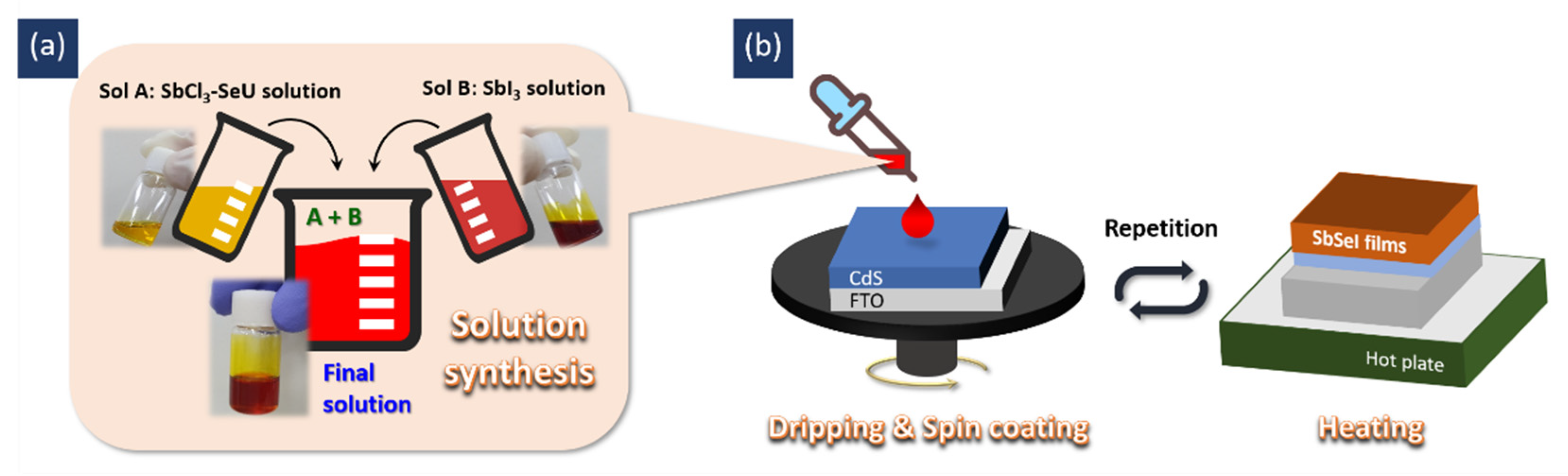
Due to the fact that SbSeI belongs to the SbSI family [13], SbSeI formation may be expressed by the following chemical reaction, similar to the case of SbSI [8,10,12,13]: Sb2Se3 + SbI3 → 3SbSeI. In addition, according to the Sb-Se-I phase diagram [14,15], the SbSeI phase is formed through a competing process of two phases, Sb2Se3 and SbI3, under controlled molar ratios and temperature conditions. These results suggest that the control of Sb2Se3 and SbI3 is a key factor in the development of a method for SbSeI fabrication. As a first step, we explored different solutions that could produce Sb2Se3 and SbI3. As a result, we found that two solutions based on SbCl3-SeU (Sol A, where SeU is selenourea) and SbI3 (Sol B) may be used to form Sb2Se3 and SbI3 phases, respectively, at a low temperature of 150 °C (as shown in Figure S1 of the Supplementary Material). Based on these findings, we developed a solution-processing method for the fabrication of SbSeI thin films. Specifically, we designed a precursor solution that may be used to produce a pure-phase film in a single step by mixing the two solutions.
In this work, we report a facile one-step solution-processing method based on precursor engineering using Sol A and Sol B solutions. The precursor solutions were synthesized by mixing Sol A and Sol B at different molar ratios. This controlled molar ratio allowed for the manipulation of Sb2Se3 and SbSeI phases, leading to the formation of a pure SbSeI film under specific conditions. Moreover, the pure phase was obtained at a low temperature of 150 °C. We also applied this approach to the fabrication of other selenoiodides, namely (Bi,Sb)SeI, to prove the versatility of the proposed method in terms of the preparation of various chalcoiodides for solar cell applications.
2. Materials and Methods
2.1. Chemical and Materials
Antimony (III) chloride (SbCl3, 99+ %), antimony (III) iodide (SbI3, 99.999%), SeU (NH2CSeNH2, 99.97%), N-methyl-2-pyrrolidinone (NMP, C5H9NO, anhydrous, 99.5%), and N,N-dimethylformamide (DMF, HCON(CH3)2, anhydrous, 99.8%) were purchased from Alfa Aesar (Seoul, Korea). Cadmium sulfate hydrate (CdSO4·8/3H2O, ≥99.0%), thiourea (TU, NH2CSNH2, ≥99.0%), and bismuth (III) iodide (BiI3, 99%) were purchased from Sigma-Aldrich (Seoul, Korea). Ammonium hydroxide solution (NH4OH, 28% NH3 in H2O) was purchased from Junsei (Tokyo, Japan). All chemicals were used as received without further purification. FTO glass with a sheet resistance of 15 Ω sq−1 was purchased from Pilkington (AMG, Yongin-si, Korea).
2.2. Preparation of the CdS/FTO Substrate
A 50 nm-thick CdS layer was deposited on the FTO glass using a chemical bath deposition method. CdS deposition was performed according to a previously reported procedure [16], in which FTO glass was dipped in an aqueous solution containing CdSO4·8/3H2O, NH4OH, and TU. During immersion, the temperature and pH of the solution were maintained at 65 °C and 11–11.5, respectively. After being dipped for 12 min 30 s, the glass was removed from the solution and washed with deionized water several times, before being dried. The sample was then immediately transferred into an N2-filled glove box with a moisture control system, in which the H2O level was maintained below 1 ppm, to anneal it in an inert gas. Finally, the CdS/FTO substrate was obtained after heating at 400 °C for 1 h in the glove box.
2.3. Synthesis of Precursor Solution and Deposition of SbSeI Thin Films
The precursor solution was synthesized by mixing two stock solutions, Sol A and Sol B, as shown in Figure 1a. In order to synthesize Sol A, 0.5 mmol SbCl3 and 1.25 mmol SeU were dissolved in 1 mL of DMF. Sol B was prepared by dissolving 0.5 mmol SbI3 in 1 mL of NMP. After stirring the two solutions for 1 h, they were mixed at different molar ratios and stirred for a further 1 h to prepare the precursor solution. After this step, 180 μL of the final solution was spin-coated at 5000 rpm on the pre-cleaned CdS/FTO substrate, followed by heating at 150 °C for 5 min (Figure 1b). This process was repeated five times, and all procedures were performed in a glove box. During solution synthesis, the CdS/FTO substrate was cleaned by UV/O3 treatment for 20 min outside the glove box, before being immediately returned to the glove box prior to spin-coating.
2.4. Characterization
Optical absorption was measured using a UV-VIS absorption spectrophotometer (Shimadzu UV-2600) in the wavelength range of 400–1200 nm. A sample crystal structure was measured using an X-ray diffractometer (Malvern Panalytical Empyrean, Malvern, UK) in the θ/2θ scan mode. The phase quantification was performed by the Rietveld method using X’Pert HighScore Plus (version 3.0.0) software. A field emission scanning electron microscope (Hitachi S-4800, Tokyo, Japan) was used to investigate sample morphology. Electronic structure was investigated by ultraviolet photoelectron spectroscopy (UPS) using an X-ray photoelectron spectrometer (Thermo Scientific ESCALAB 250Xi, Lexington, MA, USA).
3. Results and Discussion
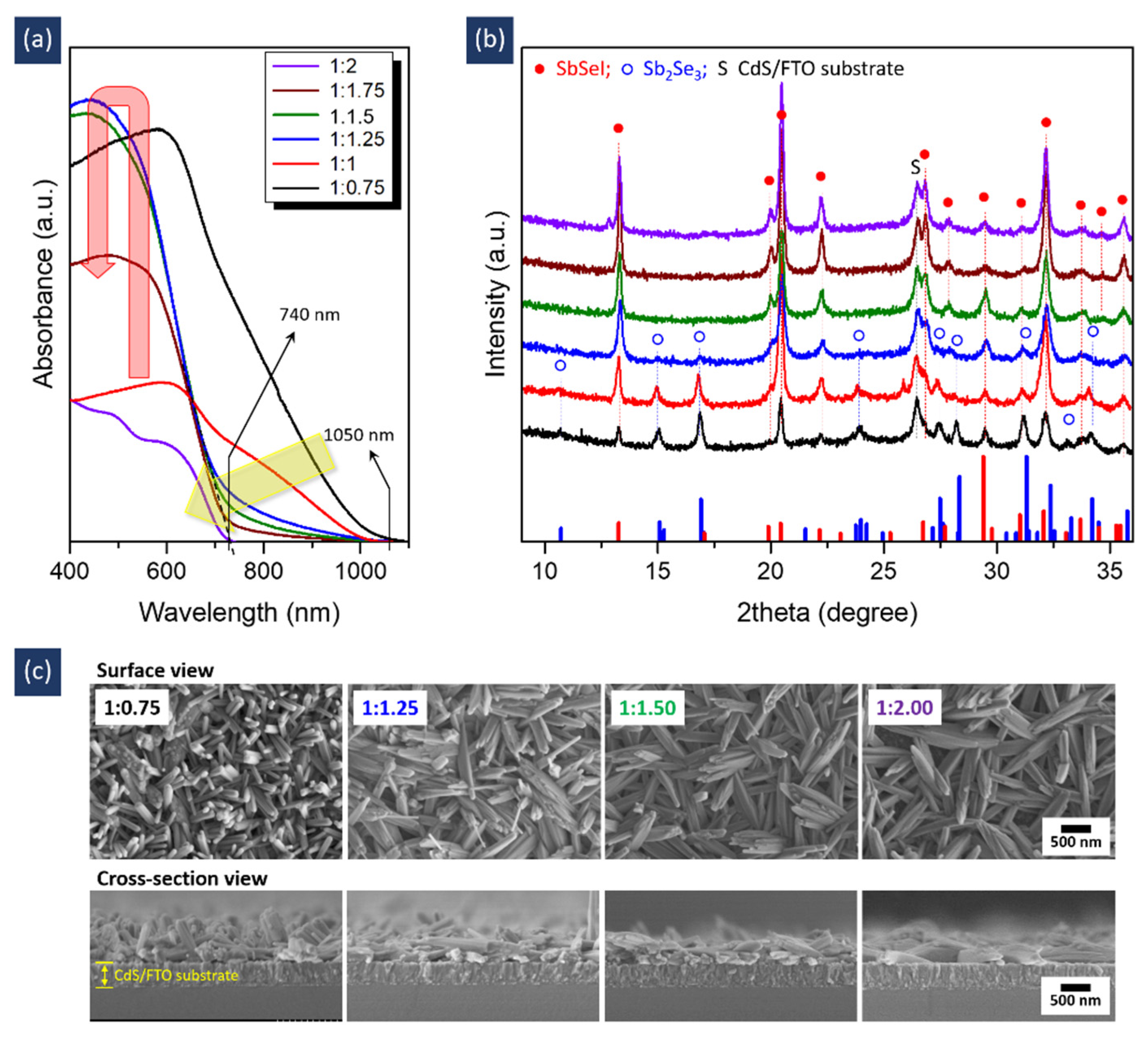
The precursor solution was synthesized by mixing Sol A and Sol B, and so it was expected that the molar ratio of Sol A and Sol B would affect film formation. To verify this hypothesis, we investigated the absorption properties, crystalline structures, and morphologies of films fabricated using precursor solutions with different Sol A:Sol B molar ratios. At a ratio of 1:0.75 (denoted as a black line in Figure 2a), an absorption edge of ~1050 nm, which is consistent with the value of Sb2Se3 [17,18], was observed. The sample also exhibited a dominant Sb2Se3 phase (ICDD # 98-065-1518), as shown in the X-ray diffraction (XRD) pattern (Figure 2b, Tables S1 and S2). Concerning the morphology shown in the field emission scanning electron microscopy (FESEM) image of Figure 2c, nanorods with a diameter of ~50 nm were found to grow randomly on the substrate. These results indicate that Sb2Se3 nanorods were mainly formed under these conditions. As the SbI3 content increased to 1:1.5, the absorption edge shifted toward a wavelength of 740 nm (bandgap EG of 1.68 eV), corresponding to the value for SbSeI [5], as indicated by the yellow arrow in Figure 2a. The absorption intensity in the short-wavelength region below 740 nm also gradually increased (denoted by a red arrow). In addition, at a molar ratio of 1:1.5, the SbSeI phase (ICDD # 98-003-1292) became dominant, whereas the Sb2Se3 phase decreased and then disappeared (Figure 2b and Table S1). As the SbI3 content increased, the nanorods aggregated to form nanostructures (Figure 2c). Furthermore, the increase in SbI3 induced a decrease in absorption intensity, although this did not affect the XRD patterns and morphology. These results imply that a nanostructured SbSeI film with high crystallinity may be fabricated at a specific molar ratio of 1:1.5.
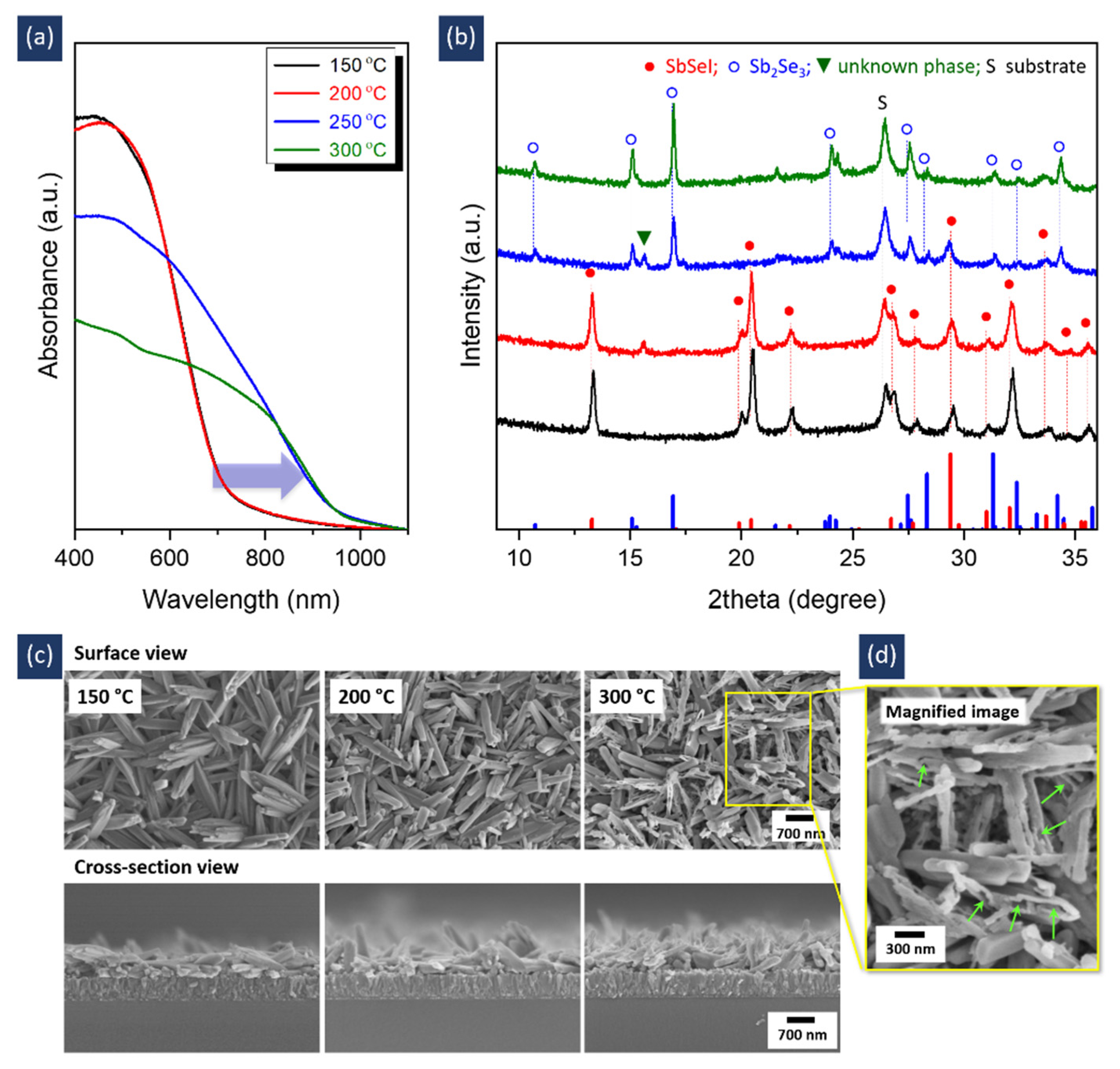
In addition to the molar ratio in the precursor solution, we found that annealing temperature played a key role in the formation of pure-phased SbSeI films, as shown in Figure 3. At a temperature of 200 °C, the absorption spectrum was almost equal to that at 150 °C (Figure 3a). However, an unknown peak (the green arrow pointing downwards in Figure 3b) appeared with a decreased SbSeI phase (Figure 3b and Table S3). Further increasing the temperature to 250 °C caused a shift in the absorption edge from 740 nm to 1050 nm (denoted as a blue arrow), revealing a phase change from SbSeI to Sb2Se3. This change was confirmed by the XRD results (Figure 3b and Table S3), in which the Sb2Se3 phase predominantly appeared when the temperature was increased to 250 °C. Note that the unknown phase may be considered to be an intermediate Sb-Se-I phase because it is formed in a temperature region where Sb2Se3 and SbSeI phases can coexist. When the temperature reached 300 °C, only XRD peaks corresponding to the Sb2Se3 phase were observed. The morphology was very similar to that at 150 °C, as shown in Figure 3c, although several voids were observed in the nanostructures, as indicated by the green arrows in the magnified image (Figure 3d). This similarity in morphology suggests that SbSeI was formed at an early stage during formation at 300 °C. However, because the SbSeI phase is unstable at a higher temperature and is prone to decomposition [14,15], SbI3 may evaporate from the initially formed SbSeI as the reaction proceeds, creating voids in the nanostructures. As a result, Sb2Se3, which is similar in morphology to SbSeI despite containing many pores, was formed. A low temperature of 150 °C was therefore required to obtain pure SbSeI films. This temperature was also confirmed by an investigation of the XRD pattern in the low-temperature region of 120–180 °C (Figure S2 of the Supplementary Material).
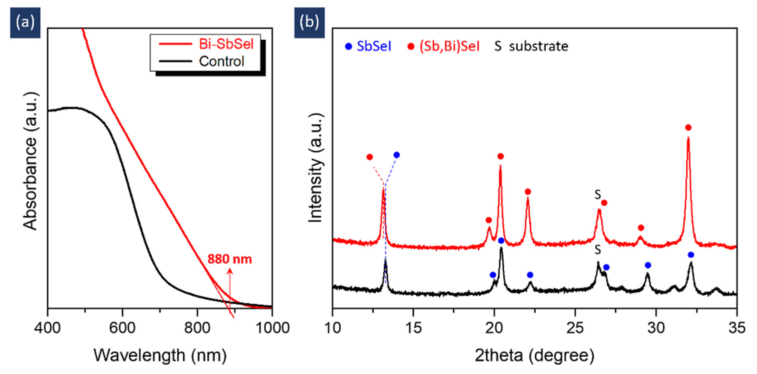
Given that the phase of the fabricated films was determined by the type of solution used in the precursor solution, it was possible to fabricate various chalcohalides by changing the starting solutions. To verify this possibility, we modified the precursor solution by introducing BiI3 instead of SbI3 and deposited it on a CdS/FTO substrate following the optimized procedures. For convenience, the sample fabricated using the optimized solution shown in Figure 2 is denoted as ‘control’ in Figure 4. The sample fabricated using the BiI3-modified solution is also denoted as ‘Bi-SbSeI’. As shown in Figure 4a, the Bi-SbSeI sample exhibits an absorption edge of ~880 nm, which corresponds to an EG of ~1.41 eV. This EG value is lower than that of SbSeI (~1.68 eV) but higher than that of BiSeI (~1.32 eV) [19,20]. Figure 4b and Table S4 show that the XRD peaks of Bi-SbSeI are located between the two references for BiSeI (ID: mp-23020, The Materials Project) [21] and SbSeI (ICDD # 98-003-1292). The detected peaks were symmetrical, indicating that a single phase was formed. Based on these results, it can be concluded that a single-phase material composed of (Bi,Sb)SeI was successfully formed by modifying the precursor solution. This suggests that the proposed method can be used to fabricate various chalcohalides, such as SbSI, BiSI, and related alloys.
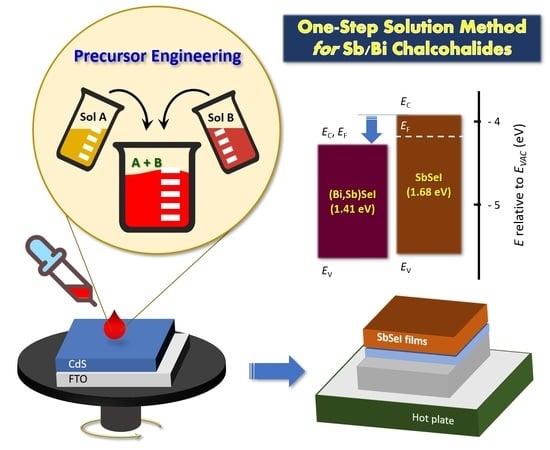
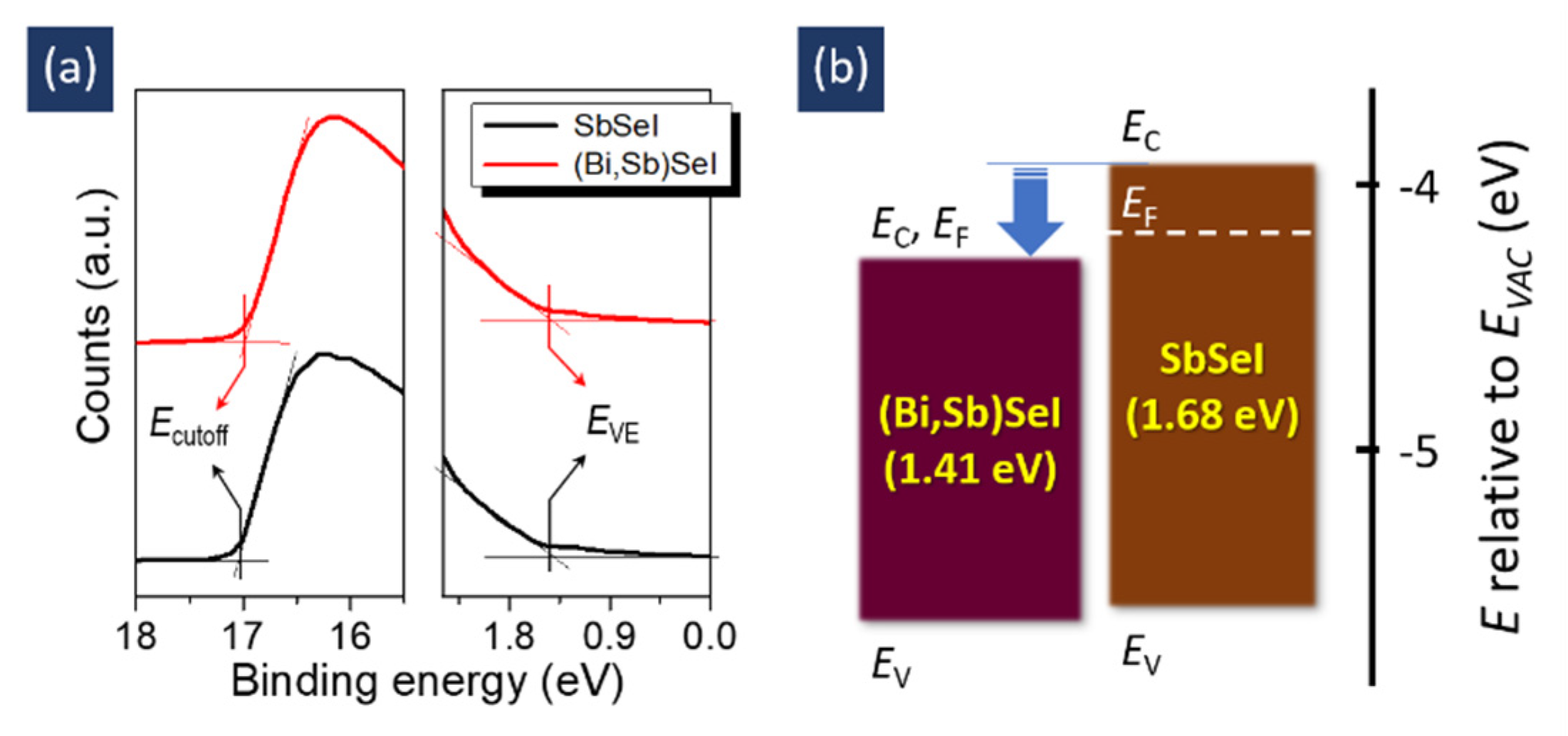
We investigated the electronic structures of the samples (shown in Figure 4) further by analyzing their UPS spectra (Figure 5a). We obtained two values from the spectra, one for the cut-off energy, Ecutoff, and another for the valence band edge energy, EVE. From the two equations EV = EF + EVE and EV = hυ − (Ecutoff − EVE), we also calculated the following three values: conduction band minimum (EC), valence band maximum (EV), and Fermi level energy (EF) [22]. These values are listed in Table S5 of the Supplementary Material and are shown in Figure 5b. The (Bi,Sb)SeI sample presented a similar EV to SbSeI, but a lower EC value. This result indicates that the incorporation of Bi into SbSeI induces a downshift in EC. This result also suggests that electronic structure may be controlled via compositional engineering. The proposed method could therefore be applied to optimizing electronic properties in order to render materials suitable for solar cell applications via compositional engineering. However, the current method is limited when it comes to forming a dense film, as shown in Figure 2c. It is generally accepted that morphology plays a key role in obtaining high efficiency [7]. Typically, dense films with a large grain size contribute significantly to achieving high performance. Thus, it can be deduced that it is very difficult to obtain a high level of efficiency from our films. A preliminary result confirmed that the device exhibited a very poor efficiency of 0.23% (Table S6 of the Supplementary Materials). Therefore, we are currently adapting the proposed method in order to both improve and optimize the morphology of SbSeI films. The morphology may be improved by various approaches, such as annealing optimization, post-treatment, the use of additive effects, and solvent annealing [7].
4. Conclusions
A simple one-step solution-processing method for the fabrication of SbSeI films is presented. The pure-phase SbSeI film (EG = 1.68 eV) was obtained at a low temperature of 150 °C using a precursor solution with a molar ratio of Sol A:Sol B = 1:1.5. Modifying the precursor solution resulted in the formation of (Bi,Sb)SeI. These results suggest that the proposed method can be readily applied to the fabrication of various chalcohalides, as well as to optimize their electronic structures in order to render them suitable for solar cell applications. However, further improvements are necessary to optimize key factors, such as morphology, crystalline orientation, and defects, so as to make them suitable for high performance Sb/Bi chalcohalide solar cells.
Supplementary Materials
The following are available online at https://0-www-mdpi-com.brum.beds.ac.uk/article/10.3390/nano11123206/s1: Figure S1: absorption spectra and XRD patterns of samples fabricated with Sol A and sol B; Table S1: Quantitative ratio of Sb2Se3 and SbSeI phases; Table S2: Lattice spacings for each phase; Table S3: Quantitative ratio of Sb2Se3, SbSeI, and unknown phases; Figure S2: XRD patterns of samples fabricated at 120–180 °C; Table S4: Comparison of XRD peaks of (Bi,Sb)SeI with references; Table S5: Ecutoff, EVE, EC, EV, and EF values of SbSI and (Bi,Sb)SeI samples; Table S6: Device parameters of the SbSeI solar cells.
Author Contributions
Conceptualization, Y.C.C.; methodology, Y.C.C.; formal analysis, Y.C.C. and K.-W.J.; investigation, Y.C.C.; writing—original draft preparation, Y.C.C.; writing—review and editing, Y.C.C. and K.-W.J.; supervision, Y.C.C.; project administration, Y.C.C. All authors have read and agreed to the published version of the manuscript.
Funding
This work was supported by the National Research Foundation of Korea (NRF) grant funded by the Korea government (MSIT) (No. 2019R1F1A1049014). This work was also supported by the DGIST R&D program of the Ministry of Science and ICT, Korea (No. 21-ET-08).
Data Availability Statement
All relevant data supporting the findings of this study are available within the article and its Supplementary Material.
Conflicts of Interest
The authors declare no conflict of interest.
References
- Nie, R.; Sumukam, R.R.; Reddy, S.H.; Banavoth, M.; Seok, S.I. Lead-free perovskite solar cells enabled by hetero-valent substitutes. Energy Environ. Sci. 2020, 13, 2363–2385. [Google Scholar] [CrossRef]
- Choi, Y.C.; Jung, K.-W. Recent Progress in Fabrication of Antimony/Bismuth Chalcohalides for Lead-Free Solar Cell Applications. Nanomaterials 2020, 10, 2284. [Google Scholar] [CrossRef]
- Huang, Y.T.; Kavanagh, S.R.; Scanlon, D.O.; Walsh, A.; Hoye, R.L.Z. Perovskite-inspired materials for photovoltaics and beyond-from design to devices. Nanotechnology 2021, 32, 132004. [Google Scholar] [CrossRef] [PubMed]
- Li, T.; Luo, S.; Wang, X.; Zhang, L. Alternative Lone-Pair ns2-Cation-Based Semiconductors beyond Lead Halide Perovskites for Optoelectronic Applications. Adv. Mater. 2021, 33, 2008574. [Google Scholar] [CrossRef]
- Nie, R.; Hu, M.; Risqi, A.M.; Li, Z.; Seok, S.I. Efficient and Stable Antimony Selenoiodide Solar Cells. Adv. Sci. 2021, 8, 2003172. [Google Scholar] [CrossRef]
- Li, D.; Zhang, D.; Lim, K.S.; Hu, Y.; Rong, Y.; Mei, A.; Park, N.G.; Han, H. A Review on Scaling Up Perovskite Solar Cells. Adv. Funct. Mater. 2021, 31, 2008621. [Google Scholar] [CrossRef]
- Tailor, N.K.; Abdi-Jalebi, M.; Gupta, V.; Hu, H.; Dar, M.I.; Li, G.; Satapathi, S. Recent progress in morphology optimization in perovskite solar cell. J. Mater. Chem. A 2020, 8, 21356–21386. [Google Scholar] [CrossRef]
- Nie, R.; Yun, H.-s.; Paik, M.-J.; Mehta, A.; Park, B.-w.; Choi, Y.C.; Seok, S.I. Efficient Solar Cells Based on Light-Harvesting Antimony Sulfoiodide. Adv. Energy Mater. 2018, 8, 1701901. [Google Scholar] [CrossRef]
- Nie, R.; Im, J.; Seok, S.I. Efficient Solar Cells Employing Light-Harvesting Sb0.67Bi0.33SI. Adv. Mater. 2019, 31, 1808344. [Google Scholar] [CrossRef]
- Choi, Y.C.; Hwang, E.; Kim, D.-H. Controlled growth of SbSI thin films from amorphous Sb2S3 for low-temperature solution processed chalcohalide solar cells. APL Mater. 2018, 6, 121108. [Google Scholar] [CrossRef] [Green Version]
- Choi, Y.C.; Hwang, E. Controlled Growth of BiSI Nanorod-Based Films Through a Two-Step Solution Process for Solar Cell Applications. Nanomaterials 2019, 9, 1650. [Google Scholar] [CrossRef] [PubMed] [Green Version]
- Jung, K.-W.; Choi, Y.C. Compositional Engineering of Antimony Chalcoiodides via a Two-Step Solution Process for Solar Cell Applications. ACS Appl. Energy Mater. 2021. [Google Scholar] [CrossRef]
- Shiozaki, Y.; Nakamura, E.; Mitsui, T. Ferroelectrics and Related Substances: Inorganic Substances other than Oxides. Part 1: SbSI Family…TAAP, 1st ed.; Springer: Berlin/Heidelberg, Germany, 2004. [Google Scholar]
- Aliev, Z.; Musaeva, S.; Babanly, D.; Shevelkov, A.; Babanly, M. Phase diagram of the Sb–Se–I system and thermodynamic properties of SbSeI. J. Alloys Compd. 2010, 505, 450–455. [Google Scholar] [CrossRef]
- Aliev, Z.S. The Av–Bvi–I Ternary Systems: A Brief Review on the Phase Equilibria Review. Condens. Matter Interphases 2019, 21, 338–349. [Google Scholar] [CrossRef]
- Yang, K.J.; Kim, S.; Kim, S.Y.; Ahn, K.; Son, D.H.; Kim, S.H.; Lee, S.J.; Kim, Y.I.; Park, S.N.; Sung, S.J.; et al. Flexible Cu2ZnSn(S,Se)4 solar cells with over 10% efficiency and methods of enlarging the cell area. Nat. Commun. 2019, 10, 2959. [Google Scholar] [CrossRef] [Green Version]
- Choi, Y.C.; Mandal, T.N.; Yang, W.S.; Lee, Y.H.; Im, S.H.; Noh, J.H.; Seok, S.I. Sb2Se3-Sensitized Inorganic-Organic Heterojunction Solar Cells Fabricated Using a Single-Source Precursor. Angew. Chem. Int. Ed. 2014, 53, 1329–1333. [Google Scholar] [CrossRef]
- Choi, Y.C.; Lee, Y.H.; Im, S.H.; Noh, J.H.; Mandal, T.N.; Yang, W.S.; Seok, S.I. Efficient Inorganic-Organic Heterojunction Solar Cells Employing Sb2(Sx/Se1-x)3 Graded-Composition Sensitizers. Adv. Energy Mater. 2014, 4, 1301680. [Google Scholar] [CrossRef]
- Chepur, D.V.; Bercha, D.M.; Tubyanitsa, I.D.; Slivka, V.Y. Peculiarities of the Energy Spectrum and Edge Absorption in the Chain Commpounds AVBVICVII. Phys. Stat. Sol. 1968, 30, 461–468. [Google Scholar] [CrossRef]
- Kunioku, H.; Higashi, M.; Abe, R. Low-Temperature Synthesis of Bismuth Chalcohalides: Candidate Photovoltaic Materials with Easily, Continuously Controllable Band gap. Sci. Rep. 2016, 6, 32664. [Google Scholar] [CrossRef]
- Jain, A.; Ong, S.P.; Hautier, G.; Chen, W.; Richards, W.D.; Dacek, S.; Cholia, S.; Gunter, D.; Skinner, D.; Ceder, G.; et al. Commentary: The Materials Project: A materials genome approach to accelerating materials innovation. APL Mater. 2013, 1, 011002. [Google Scholar] [CrossRef] [Green Version]
- Shao, G. Work Function and Electron Affinity of Semiconductors: Doping Effect and Complication due to Fermi Level Pinning. Energy Environ. Mater. 2021, 4, 273–276. [Google Scholar] [CrossRef]
Figure 1.
Schematic illustrations of (a) the synthesis of the one-step solution, and (b) the deposition process for SbSeI thin films.
Figure 1.
Schematic illustrations of (a) the synthesis of the one-step solution, and (b) the deposition process for SbSeI thin films.

Figure 2.
(a) Absorption spectra, (b) XRD patterns, and (c) FESEM images of samples prepared using precursor solutions with different Sol A:Sol B molar ratios. The peak positions of Sb2Se3 and SbSeI are shown in (b), based on the reference data of Sb2Se3 (ICDD # 98-065-1518, blue column) and SbSeI (ICDD # 98-003-1292, red column).

Figure 3.
(a) Absorption spectra, (b) XRD patterns, and (c) FESEM images of samples prepared at different annealing temperatures. (d) Magnified image, marked by a yellow box in (c). All samples were fabricated using the precursor solution with a Sol A:Sol B molar ratio of 1:1.5. In (b), two reference patterns of Sb2Se3 ((ICDD # 98-065-1518) and SbSeI (ICDD # 98-003-1292) are shown as blue columns and red columns, respectively.

Figure 4.
(a) Absorption spectra and (b) XRD patterns of control and Bi-SbSeI samples.

Figure 5.
(a) UPS spectra of SbSI and (Bi,Sb)SeI, and (b) the derived energy level diagram.

Publisher’s Note: MDPI stays neutral with regard to jurisdictional claims in published maps and institutional affiliations. |
© 2021 by the authors. Licensee MDPI, Basel, Switzerland. This article is an open access article distributed under the terms and conditions of the Creative Commons Attribution (CC BY) license (https://creativecommons.org/licenses/by/4.0/).
Share and Cite
MDPI and ACS Style
Choi, Y.C.; Jung, K.-W. One-Step Solution Deposition of Antimony Selenoiodide Films via Precursor Engineering for Lead-Free Solar Cell Applications. Nanomaterials 2021, 11, 3206. https://0-doi-org.brum.beds.ac.uk/10.3390/nano11123206
AMA Style
Choi YC, Jung K-W. One-Step Solution Deposition of Antimony Selenoiodide Films via Precursor Engineering for Lead-Free Solar Cell Applications. Nanomaterials. 2021; 11(12):3206. https://0-doi-org.brum.beds.ac.uk/10.3390/nano11123206
Chicago/Turabian StyleChoi, Yong Chan, and Kang-Won Jung. 2021. "One-Step Solution Deposition of Antimony Selenoiodide Films via Precursor Engineering for Lead-Free Solar Cell Applications" Nanomaterials 11, no. 12: 3206. https://0-doi-org.brum.beds.ac.uk/10.3390/nano11123206
Note that from the first issue of 2016, this journal uses article numbers instead of page numbers. See further details here.