
Synthesis of Boron Nitride Nanotubes Using Plasma-Assisted CVD Catalyzed by Cu Nanoparticles and Oxygen

 , , and
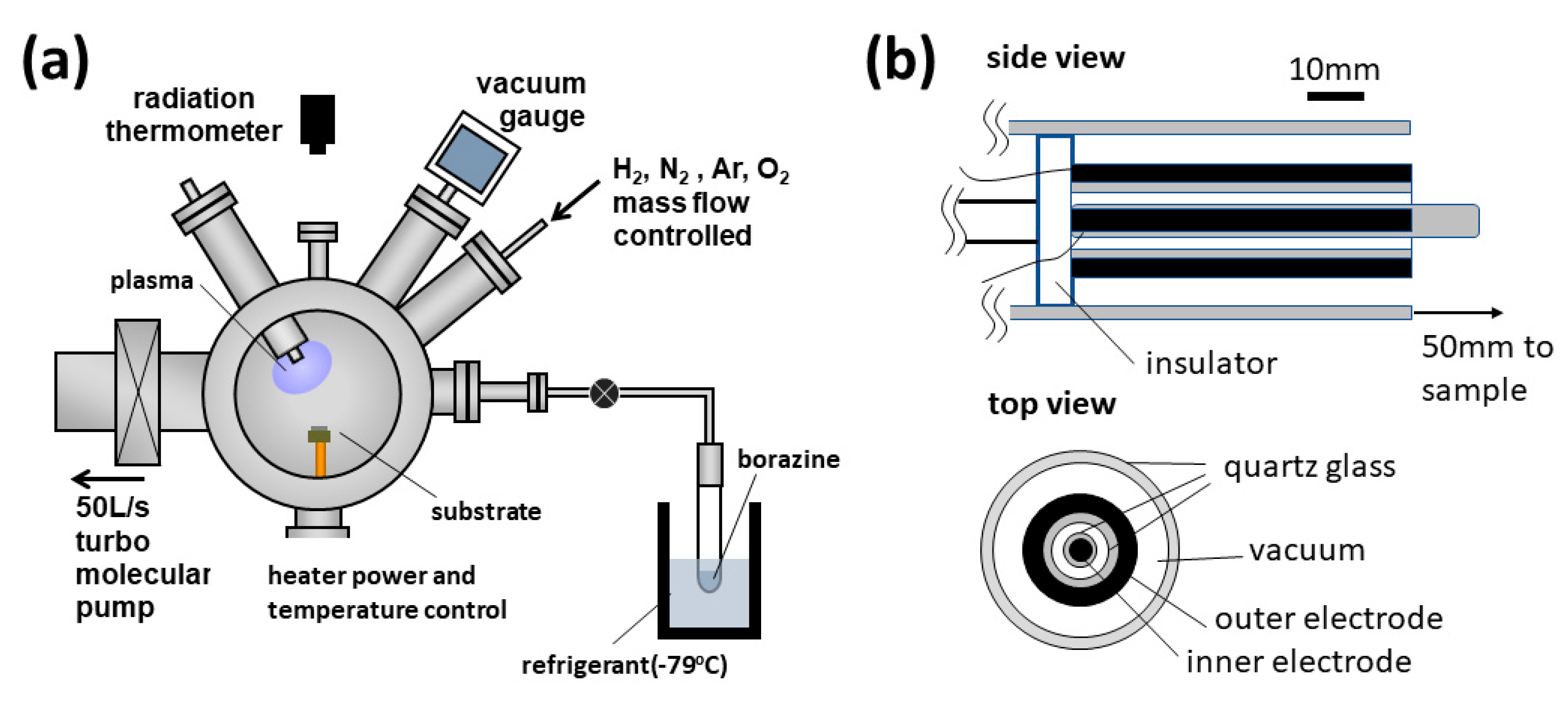
Abstract
:1. Introduction
2. Materials and Methods
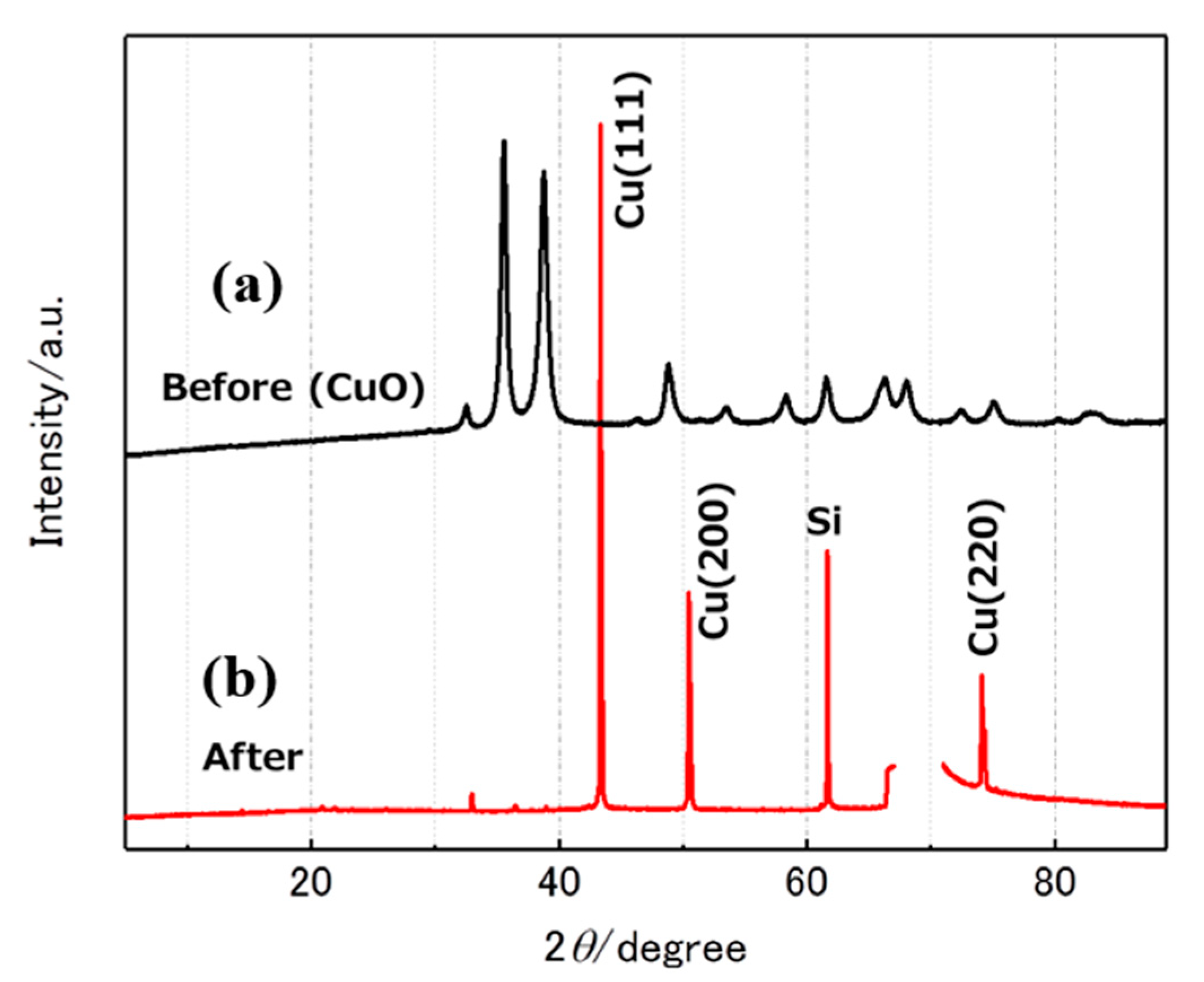
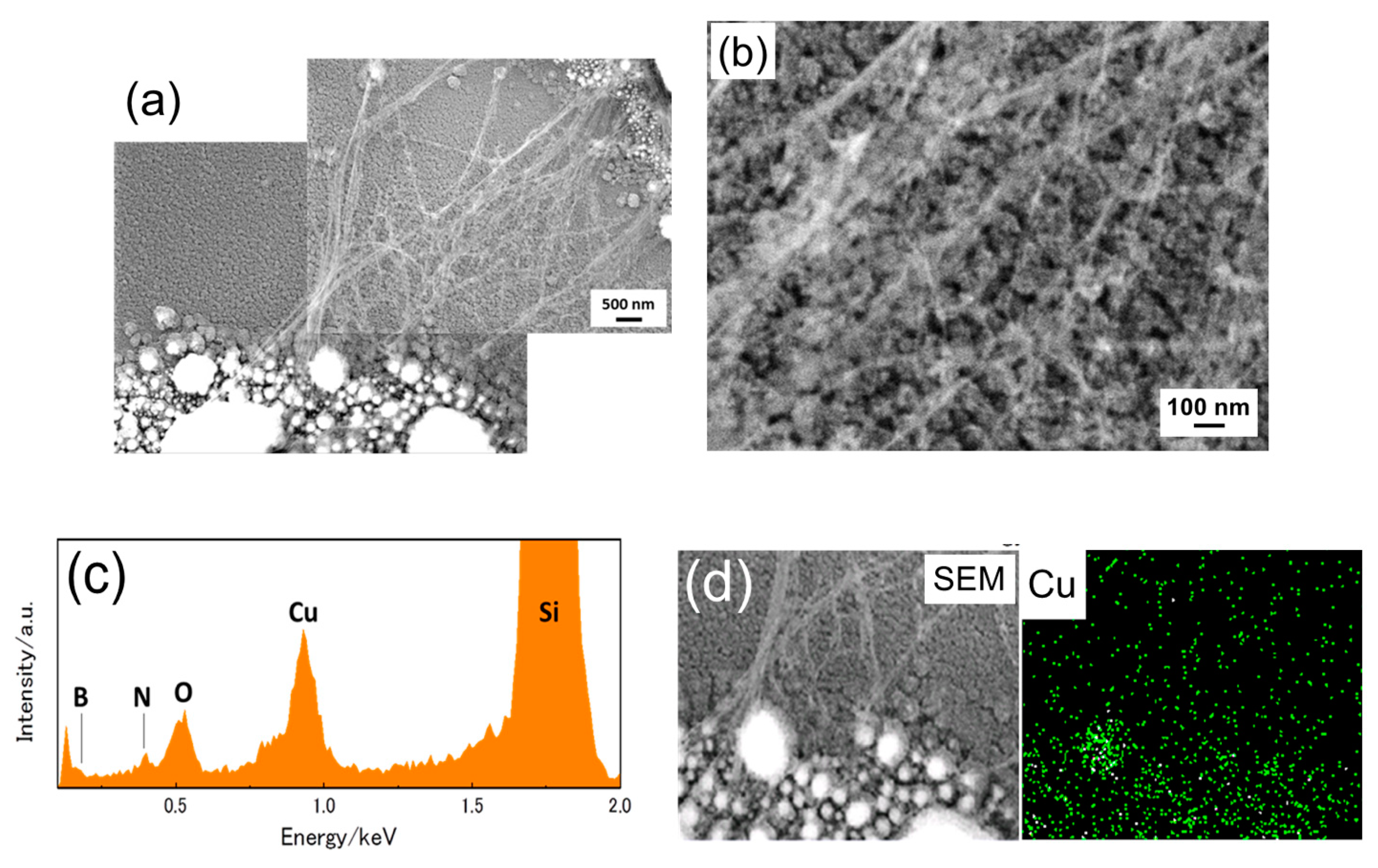
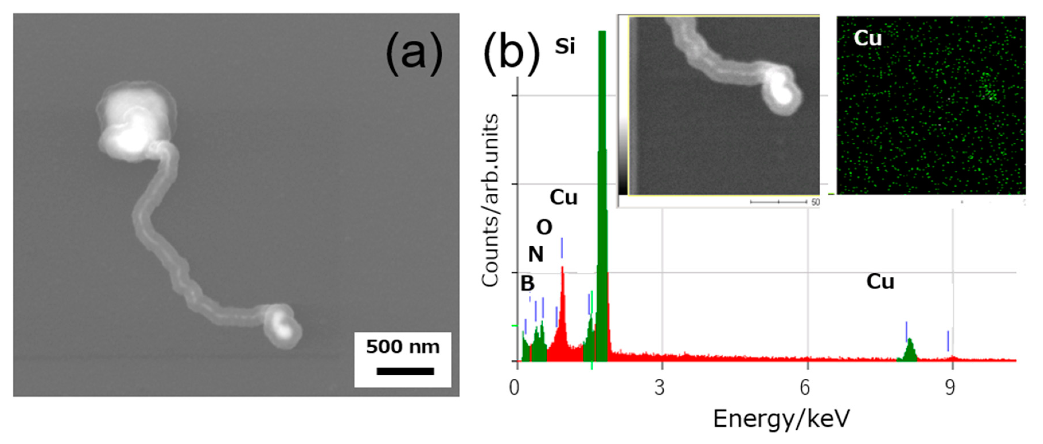
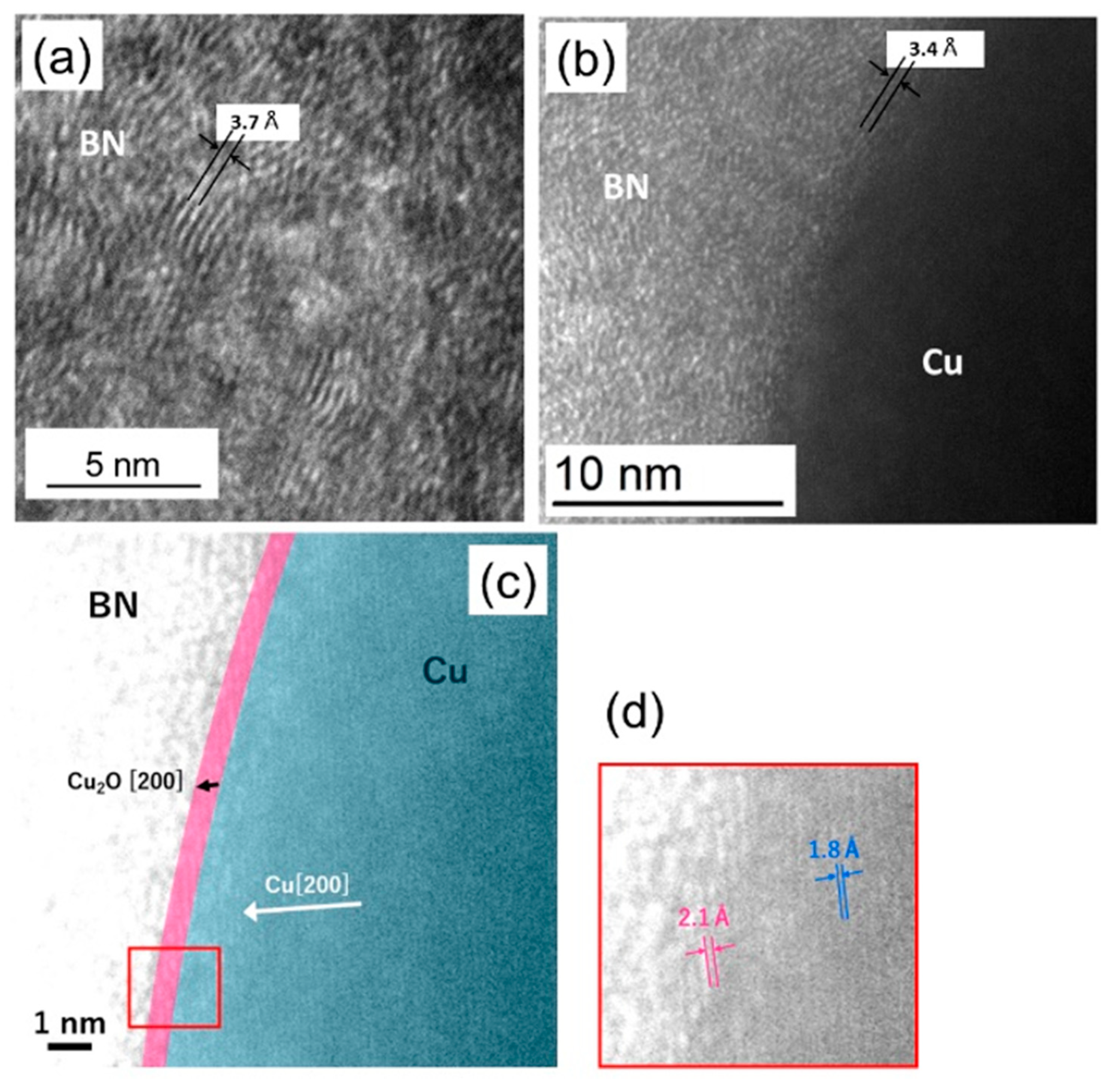
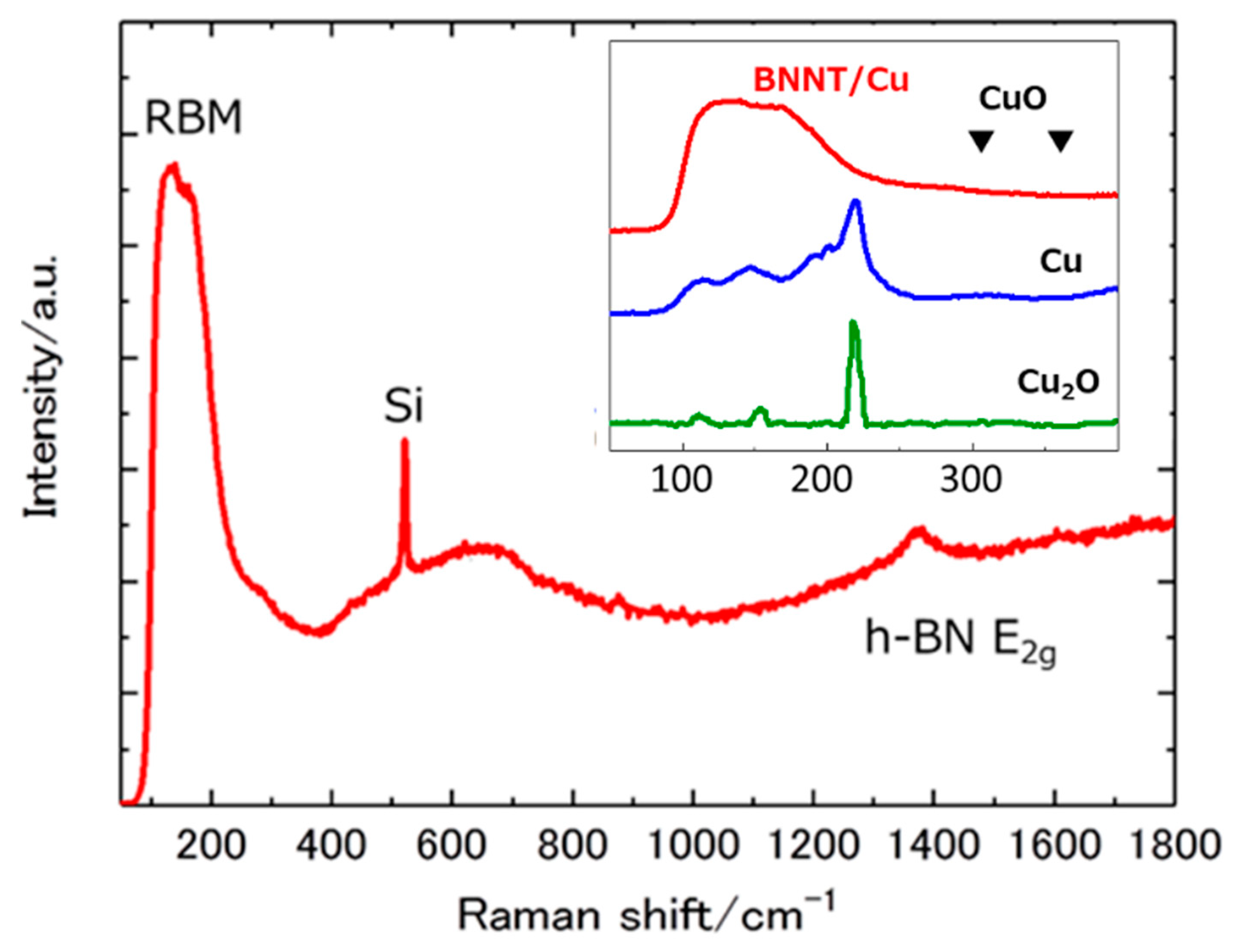
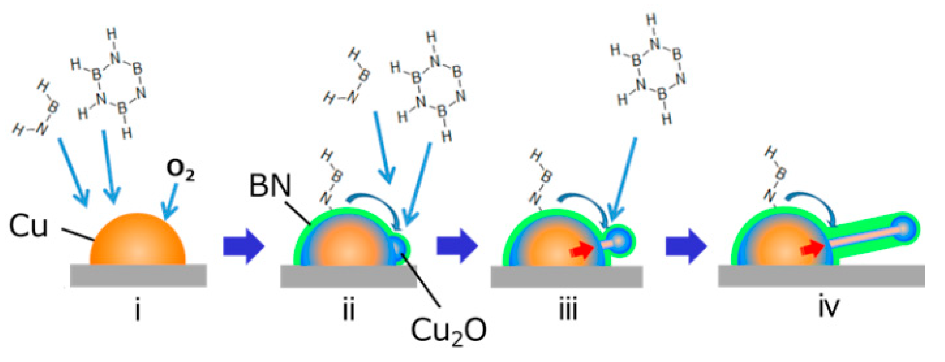
3. Results and Discussion
4. Conclusions
Author Contributions
Funding
Institutional Review Board Statement
Informed Consent Statement
Data Availability Statement
Conflicts of Interest
References
- Golberg, D.; Bando, Y.; Tang, C.; Zni, C. Boron Nitride Nanotubes. Adv. Mater. 2007, 19, 2413–2432. [Google Scholar] [CrossRef]
- Chopra, N.G.; Luyken, R.J.; Cherrey, K.; Crespi, V.H.; Cohen, M.L.; Louie, S.G.; Zettl, A. Boron Nitride Nanotubes. Science 1995, 269, 966–967. [Google Scholar] [CrossRef] [PubMed]
- Golberg, D.; Bando, Y.; Huang, Y.; Terao, T.; Mitome, M.; Tang, C.; Zhi, C. Boron Nitride Nanotubes and Nanosheets. ACS Nano 2010, 4, 2979–2993. [Google Scholar] [CrossRef]
- Bai, X.; Golberg, D.; Bando, Y.; Zhi, C.; Tang, C.; Mitome, M.; Kurashima, K. Deformation-Driven Electrical Transport of Individual Boron Nitride Nanotubes. Nano Lett. 2007, 7, 632–637. [Google Scholar] [CrossRef]
- Zettl, A.; Chopra, N.G. Measurement of the Elastic Modulus of a Multi Wall Boron Nitride Nanotube. Solid State Commun. 1998, 105, 297–300. [Google Scholar]
- Chen, Y.; Zou, J.; Campbell, S.J.; Le Caer, G. Boron Nitride Nanotubes: Pronounced Resistance to Oxidation. Appl. Phys. Lett. 2004, 84, 2430–2432. [Google Scholar] [CrossRef] [Green Version]
- Kang, J.H.; Sauti, G.; Park, C.; Yamakov, V.I.; Wise, K.E.; Lowther, S.E.; Fay, C.C.; Thibeault, S.A.; Bryant, R.G. Multifunctional Electroactive Nanocomposites Based on Piezoelectric Boron Nitride Nanotubes. ACS Nano 2015, 9, 11942–11950. [Google Scholar] [CrossRef] [PubMed]
- Jhi, S.H.; Kwon, Y.K. Hydrogen Adsorption on Boron Nitride Nanotubes: A Path to Room-Temperature Hydrogen Storage. Phys. Rev. B Condens. Matter Mater. Phys. 2004, 69, 245407. [Google Scholar] [CrossRef] [Green Version]
- Loiseau, A.; Willaime, F.; Demoncy, N.; Hug, G.; Pascard, H. Boron Nitride Nanotubes with Reduced Numbers of Layers Synthesized by Arc Discharge. Phys. Rev. Lett. 1996, 76, 4737–4740. [Google Scholar] [CrossRef] [PubMed]
- Arenal, R.; Ferrari, A.C.; Reich, S.; Wirtz, L.; Mevellec, J.Y.; Lefrant, S.; Rubio, A.; Loiseau, A. Raman Spectroscopy of Single-Wall Boron Nitride Nanotubes. Nano Lett. 2006, 6, 1812–1816. [Google Scholar] [CrossRef]
- Arenal, R.; Stephan, O.; Cochon, J.L.; Loiseau, A. Root-Growth Mechanism for Single-Walled Boron Nitride Nanotubes in Laser Vaporization Technique. J. Am. Chem. Soc. 2007, 129, 16183–16189. [Google Scholar] [CrossRef]
- Smith, M.W.; Jordan, K.C.; Park, C.; Kim, J.W.; Lillehei, P.T.; Crooks, R.; Harrison, J.S. Very Long Single-and Few-Walled Boron Nitride Nanotubes via the Pressurized Vapor/Condenser Method. Nanotechnology 2009, 20, 505604. [Google Scholar] [CrossRef]
- Chen, Y.; Chadderton, L.T.; Gerald, J.F.; Williams, J.S. A Solid-State Process for Formation of Boron Nitride Nanotubes. Appl. Phys. Lett. 1999, 74, 2960–2962. [Google Scholar] [CrossRef] [Green Version]
- Lourie, O.R.; Jones, C.R.; Bartlett, B.M.; Gibbons, P.C.; Ruoff, R.S.; Buhro, W.E. CVD Growth of Boron Nitride Nanotubes. Chem. Mater. 2000, 12, 1808–1810. [Google Scholar] [CrossRef]
- Myung, J.K.; Chatterjee, S.; Seung, M.K.; Stach, E.A.; Bradley, M.G.; Pender, M.J.; Sneddon, L.G.; Maruyama, B. Double-Walled Boron Nitride Nanotubes Grown by Floating Catalyst Chemical Vapor Deposition. Nano Lett. 2008, 8, 3298–3302. [Google Scholar]
- Ma, R.; Bando, Y.; Sato, T.; Kurashima, K. Growth, Morphology, and Structure of Boron Nitride Nanotubes. Chem. Mater. 2001, 13, 2965–2971. [Google Scholar] [CrossRef]
- Wang, H.; Wanga, H.; Wang, H.; Zhang, F.; Li, Y.; Fua, Z. Urchin-like Boron Nitride Hierarchical Structure Assembled by Nanotubes-Nanosheets for Effective Removal of Heavy Metal Ions. Ceram. Int. 2018, 44, 12216–12224. [Google Scholar] [CrossRef]
- Wang, Y.; Yamamoto, Y.; Kiyono, H.; Shimada, S. Highly Ordered Boron Nitride Nanotube Arrays with Controllable Texture from Ammonia Borane by Template-Aided Vapor-Phase Pyrolysis. J. Nanomater. 2008, 2008, 606283. [Google Scholar] [CrossRef] [Green Version]
- Zhang, D.; Zhang, K.; Songfeng, E.; Liu, D.; Li, C.; Yao, Y. The MgB2-Catalyzed Growth of Boron Nitride Nanotubes using B/MgO as a Boron Containing Precursor. Nanoscale Adv. 2020, 2, 2731. [Google Scholar] [CrossRef]
- Baysal, M.; Bilge, K.; Yildizhan, M.M.; Yorulmaz, Y.; Öncel, Ç.; Papila, M.; Yürüm, Y. Catalytic Synthesis of Boron Nitride Nanotubes at Low Temperatures. Nanoscale 2018, 10, 4658–4662. [Google Scholar] [CrossRef] [PubMed]
- Golberg, D.; Bando, Y.; Kurashima, K.; Sato, T. Ropes of BN Multi-Walled Nanotubes. Solid State Commun. 2000, 116, 1–6. [Google Scholar] [CrossRef]
- Kumar, V.; Maity, P.C.; Lahiri, D.; Lahiri, I. Copper Catalyzed Growth of Hexagonal Boron Nitride Nanotubes on a Tungsten Substrate. CrystEngComm 2018, 20, 2713–2719. [Google Scholar] [CrossRef]
- Kim, K.S.; Kingston, C.T.; Hrdina, A.; Jakubinek, M.B.; Guan, J.; Plunkett, M.; Simard, B. Hydrogen-Catalyzed, Pilot-Scale Production of Small-Diameter Boron Nitride Nanotubes and Their Macroscopic Assemblies. ACS Nano 2014, 8, 6211–6220. [Google Scholar] [CrossRef] [PubMed]
- Chatterjee, S.; Kim, M.J.; Zakharov, D.N.; Kim, S.M.; Stach, E.A.; Maruyama, B.; Sneddon, L.G. Syntheses of Boron Nitride Nanotubes from Borazine and Decaborane Molecular Precursors by Catalytic Chemical Vapor Deposition with a Floating Nickel Catalyst. Chem. Mater. 2012, 24, 2872–2879. [Google Scholar] [CrossRef]
- Su, C.Y.; Chu, W.Y.; Juang, Z.Y.; Chen, K.F.; Cheng, B.M.; Chen, F.R.; Leou, K.C.; Tsai, C.H. Large-Scale Synthesis of Boron Nitride Nanotubes with Iron-Supported Catalysts. J. Phys. Chem. C 2009, 113, 14732–14738. [Google Scholar] [CrossRef]
- Xie, M.; Wang, J.; Yap, Y.K. Mechanism for Low Temperature Growth of Boron Nitride Nanotubes. J. Phys. Chem. C 2010, 114, 16236–16241. [Google Scholar] [CrossRef]
- Cai, P.; Chen, L.; Shi, L.; Yang, Z.; Zhao, A.; Gu, Y.; Huang, T.; Qian, Y. One Convenient Synthesis Route to Boron Nitride Nanotube. Solid State Commun. 2005, 133, 621–623. [Google Scholar] [CrossRef]
- Dai, J.; Xu, L.; Fang, Z.; Sheng, D.; Guo, Q.; Ren, Z.; Wang, K.; Qian, Y. A Convenient Catalytic Approach to Synthesize Straight Boron Nitride Nanotubes Using Synergic Nitrogen Source. Chem. Phys. Lett. 2007, 440, 253–258. [Google Scholar] [CrossRef]
- Lee, K.H.; Shin, H.J.; Lee, J.; Lee, I.Y.; Kim, G.H.; Choi, J.Y.; Kim, S.W. Large-Scale Synthesis of High-Quality Hexagonal Boron Nitride Nanosheets for Large-Area Graphene Electronics. Nano Lett. 2012, 12, 714–718. [Google Scholar] [CrossRef]
- Wang, L.; Xu, X.; Zhang, L.; Qiao, R.; Wu, M.; Wang, Z.; Zhang, S.; Liang, J.; Zhang, Z.; Zhang, Z.; et al. Epitaxial Growth of a 100-Square-Centimetre Single-Crystal Hexagonal Boron Nitride Monolayer on Copper. Nature 2019, 570, 91–95. [Google Scholar] [CrossRef]
- Wideman, T.; Sneddon, L.G. Convenient Procedures for the Laboratory Preparation of Borazine. Inorg. Chem. 1995, 34, 1002–1003. [Google Scholar] [CrossRef]
- Medlin, D.L.; Friedmann, T.A.; Mirkarimi, P.B.; Rez, P.; Mills, M.J.; McCarty, K.F. Microstructure of Cubic Boron-Nitride Thin-Films Grown by Ion-Assisted Pulsed-Laser Deposition. J. Appl. Phys. 1994, 76, 295–303. [Google Scholar] [CrossRef]
- Restori, R.; Schwarzenbach, D. Charge Density in Cuprite, Cu2O. Acta Crystallogr. Sect. B Struct. Sci. 1986, B42, 201–208. [Google Scholar] [CrossRef]
- Fakrach, B.; Rahmani, A.H.; Chadli, H.; Sbai, K.; Hermet, P.; Rahmani, A. Raman-Active Modes in Finite and Infinite Double-Walled Boron Nitride Nanotubes. J. Phys. Chem. C 2015, 119, 13306–13313. [Google Scholar] [CrossRef]
- Lee, R.S.; Gavillet, J.; Chapelle, M.L.; Loiseau, A.; Cochon, J.L.; Pigache, D.; Thibault, J.; Willaime, F. Catalyst-Free Synthesis of Boron Nitride Single-Wall Nanotubes with a Preferred Zig-Zag Configuration. Phys. Rev. B Condens. Matter Mater. Phys. 2001, 64, 121405. [Google Scholar] [CrossRef]
- Narang, S.N.; Kartha, V.B.; Patel, N.D.; Solache-Carranco, H.; Juárez-Díaz, G.; Esparza-García, A.; Briseño-García, M.; Galván-Arellano, M.; Martínez-Juárez, J.; Romero-Paredes, G.; et al. Photoluminescence and X-Ray Diffraction Studies on Cu2O. J. Lumin. 1992, 204, 8–14. [Google Scholar]
- Irwin, J.C.; Chrzanowski, J.; Wei, T.; Lockwood, D.J.; Wold, A. Raman Scattering from Single Crystals of Cupric Oxide. Phys. C Supercond. Appl. 1990, 166, 456–464. [Google Scholar] [CrossRef]
- Jeon, G.S.; Mahan, G.D. Lattice Vibrations of a Single-Wall Boron Nitride Nanotube. Phys. Rev. B Condens. Matter Mater. Phys. 2009, 79, 39–41. [Google Scholar] [CrossRef]
- Fan, S.; Chapline, M.G.; Franklin, N.R.; Tombler, T.W.; Cassell, A.M.; Dai, H. Self-Oriented Regular Arrays of Carbon Nanotubes and Their Field Emission Properties. Science 1999, 283, 512–514. [Google Scholar] [CrossRef]
- Kumar, M.; Ando, Y. Chemical Vapor Deposition of Carbon Nanotubes: A Review on Growth Mechanism and Mass Production. J. Nanosci. Nanotechnol. 2010, 10, 3739–3758. [Google Scholar] [CrossRef] [Green Version]
- Chandrakumar, K.R.S.; Readle, J.D.; Rouleau, C.; Puretzky, A.; Geohegan, D.B.; More, K.; Krishnan, V.; Tian, M.K.; Duscher, G.; Sumpter, B.; et al. High-Temperature Transformation of Fe-Decorated Single-Wall Carbon Nanohorns to Nanooysters: A Combined Experimental and Theoretical Study. Nanoscale 2013, 5, 1849–1857. [Google Scholar] [CrossRef]
- Weissker, U.; Hampel, S.; Leonhardt, A.; Büchner, B. Carbon Nanotubes Filled with Ferromagnetic Materials. Materials 2010, 3, 4387–4427. [Google Scholar] [CrossRef] [Green Version]
- Lagrow, A.P.; Ward, M.R.; Lloyd, D.C.; Gai, P.L.; Boyes, E.D. Visualizing the Cu/Cu2O Interface Transition in Nanoparticles with Environmental Scanning Transmission Electron Microscopy. J. Am. Chem. Soc. 2017, 139, 179–185. [Google Scholar] [CrossRef] [PubMed]
- Bergmann, A.; Roldan Cuenya, B. Operando Insights into Nanoparticle Transformations during Catalysis. ACS Catal. 2019, 9, 10020–10043. [Google Scholar] [CrossRef] [Green Version]
- Yang, W.C.; Zeman, M.; Ade, H.; Nemanich, R.J. Attractive Migration and Coalescence: A Significant Process in the Coarsening of TiO2 Islands on the Si(111) Surface. Phys. Rev. Lett. 2003, 90, 136102. [Google Scholar] [CrossRef] [PubMed] [Green Version]
- Lee, U.; Han, Y.; Lee, S.; Kim, J.S.; Lee, Y.H.; Kim, U.J.; Son, H. Time Evolution Studies on Strain and Doping of Graphene Grown on a Copper Substrate Using Raman Spectroscopy. ACS Nano 2020, 14, 919–926. [Google Scholar] [CrossRef] [PubMed]
- Al-Kamiyani, S.; Mohiuddin, T. Effect of Copper Substrate Oxidation and Crystals Orientations on Nucleation of Triangular Graphene Domains. Vacuum 2020, 176, 109312. [Google Scholar] [CrossRef]


Publisher’s Note: MDPI stays neutral with regard to jurisdictional claims in published maps and institutional affiliations. |
© 2021 by the authors. Licensee MDPI, Basel, Switzerland. This article is an open access article distributed under the terms and conditions of the Creative Commons Attribution (CC BY) license (http://creativecommons.org/licenses/by/4.0/).
Share and Cite
Shiratori, T.; Yamane, I.; Nodo, S.; Ota, R.; Yanase, T.; Nagahama, T.; Yamamoto, Y.; Shimada, T. Synthesis of Boron Nitride Nanotubes Using Plasma-Assisted CVD Catalyzed by Cu Nanoparticles and Oxygen. Nanomaterials 2021, 11, 651. https://0-doi-org.brum.beds.ac.uk/10.3390/nano11030651
Shiratori T, Yamane I, Nodo S, Ota R, Yanase T, Nagahama T, Yamamoto Y, Shimada T. Synthesis of Boron Nitride Nanotubes Using Plasma-Assisted CVD Catalyzed by Cu Nanoparticles and Oxygen. Nanomaterials. 2021; 11(3):651. https://0-doi-org.brum.beds.ac.uk/10.3390/nano11030651
Chicago/Turabian StyleShiratori, Tatsuya, Ichiro Yamane, Shoto Nodo, Ryo Ota, Takashi Yanase, Taro Nagahama, Yasunori Yamamoto, and Toshihiro Shimada. 2021. "Synthesis of Boron Nitride Nanotubes Using Plasma-Assisted CVD Catalyzed by Cu Nanoparticles and Oxygen" Nanomaterials 11, no. 3: 651. https://0-doi-org.brum.beds.ac.uk/10.3390/nano11030651