
Electromagnetically Induced Transparency-Like Effect by Dark-Dark Mode Coupling

Department of Physics, Dalian University of Technology, Ganjingzi District, Dalian 116024, China
*
Author to whom correspondence should be addressed.
Nanomaterials 2021, 11(5), 1350; https://0-doi-org.brum.beds.ac.uk/10.3390/nano11051350
Submission received: 20 April 2021
/
Revised: 14 May 2021
/
Accepted: 17 May 2021
/
Published: 20 May 2021
(This article belongs to the Special Issue Nonlinear and Quantum Optics with Nanostructures)
Abstract
:Electromagnetically induced transparency-like (EIT-like) effect is a promising research area for applications of slow light, sensing and metamaterials. The EIT-like effect is generally formed by the destructive interference of bright-dark mode coupling and bright-bright mode coupling. There are seldom reports about EIT-like effect realized by the coupling of two dark modes. In this paper, we numerically and theoretically demonstrated that the EIT-like effect is achieved through dark-dark mode coupling of two waveguide resonances in a compound nanosystem with metal grating and multilayer structure. If we introduce , and to represent the surface plasmon polaritons (SPPs) resonance, waveguide resonance in layer 2, and waveguide resonance in layer 4, the destructive interference occurs between two pathways of and , where is the ground state without excitation. Our work will stimulate more studies on EIT-like effect with dark-dark mode coupling in other systems.
1. Introduction
The concept of electromagnetically induced transparency (EIT) was first observed in a three-level atomic system. It refers to a quantum destructive interference between two transition processes of atoms tuned by a probe and a driven laser beam, generating a narrow transparency window in a broad opaque spectrum [1]. The EIT is always accompanied by extreme spectral dispersion property, which empowers it with high potential applications in sensitive sensing [2,3], slow light [4,5,6] and metamaterials [7,8]. However, traditional EIT in atoms often requires harsh experimental conditions, such as cryogenic temperature or high intensity laser, thus restricting the practical applications of EIT [9]. By further analyzing the physics behind EIT, researchers found that the EIT can be reproduced through non-quantum approaches, such as using coupled harmonic oscillators [10] or coupled RLC electric circuits [11]. The EIT in non-quantum systems is called electromagnetically induced transparency-like (EIT-like) effect, in analogue to the EIT in atoms. The physical mechanism leads to the realization of EIT-like effect in a number of classical optical systems, for example, waveguide [12,13], photonic crystal structure [14,15], plasmonic nanosystem [16,17,18], and metasurface [19,20], in which the conditions for implementing EIT are not so strict as those in an atomic system. The EIT-like effect is reported for a wide frequency range, from microwave [21], terahertz [22,23], infrared [24,25] to optical frequencies [26]. Recently, the EIT-like effect on metasurfaces has raised intensive attention. Li et al. theoretically and experimentally proposed an actively controlled EIT-like effect in the THz regime on a metasurface using phase change material of vanadium dioxide (VO2). The metasurface is composed of meanderline and U-shaped resonators [27]. Xiao et al. designed a graphene-based metasurface, which can exhibit a tunable EIT-like effect at mid-infrared frequency. The EIT-like effect is formed by the coupling of the quadrupole mode of the nano-strip and the dipole mode of the nano-disks [28]. Chen et al. theoretically demonstrated an EIT-like effect at THz frequency on a metasurface, comprising an outer circular ring resonator made by graphene, an inner vertical two-gap circular split ring resonator (VSRR) and a smaller horizontal two-gap circular split ring resonator (HSRR) [29]. Yang et al. proposed a metasurface consisting of a cut-wire and a side coupled split-ring resonator. The metasurface incorporates both EIT-like effect and polarization conversion at THz frequency [30].
Generally, the EIT-like effect in various systems is achieved through (i) bright-dark mode coupling and (ii) bright–bright mode coupling. In the bright-dark mode coupling, the bright mode is a result of direct interaction with the external field and usually processes a low-Q factor. The dark mode does not couple to the external field and is induced by the bright mode through near-field coupling. The dark mode is a high-Q factor resonance. When the bright and dark mode get close to each other at the same resonant frequency, destructive interference between the two modes occurs and an EIT-like effect is generated. Most EIT-like effects reported are of this kind [8,10,16,31,32,33,34]. In the bright-bright mode coupling, the EIT-like effect is realized by breaking the symmetry or varying the lateral distance of two bright modes [35,36,37,38]. Although EIT-like effect has been studied intensively, the EIT-like effect achieved by two dark modes has been seldom reported. Pitchappa et al. reported the active control of EIT-like effect at THz frequency with the excitation of a dual pathway of dark split ring resonators (SRRs) on a metasurface [39]. However, the EIT-like effect with dark-dark mode coupling at visible frequency has not been reported yet.
In this work, we report the EIT-like effect at visible frequency with dark-dark mode coupling of two waveguide resonances in a compound nanosystem. Although we also report the dark-dark mode coupling, our work is different from the work of Pitchappa et al. in structure, frequency and the resonances for coupling. The nanosystem is composed of metal grating and multilayer structure. If we introduce , and to represent the surface plasmon polaritons (SPPs) resonance, waveguide resonance in layer 2, and waveguide resonance in layer 4, the destructive interference occurs between two pathways of and , where is the ground state without excitation. The formation process of the EIT-like effect is demonstrated by simulated field distributions and theoretical results derived from equations. We further investigate the influences of grating period, grating width, grating thickness, thicknesses of different layers, and refractive indices of different layers on the EIT-like effect. We believe that our work will inspire more studies of EIT-like effect with dark-dark mode coupling in other systems.
2. Structure and Theory
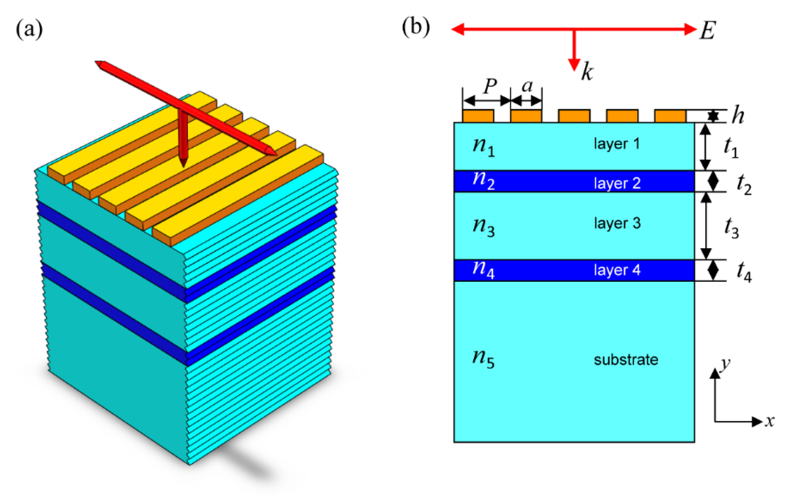
The proposed nanosystem is composed of a gold (Au) grating and a multilayer structure with the schematic map shown in Figure 1. The Au grating is defined by its period , grating width and thickness . The multilayer structure contains four layers and a substrate with refractive indices illustrated in Figure 1b. The thicknesses of the four layers are described by , , and . We choose a Cytop fluoropolymer material for layer 1, layer 3 and the substrate with a permittivity of [40]. Additionally, a TiO2 material is employed in layer 2 and layer 4 with refractive indices of .
The dispersive permittivity of Au is described by a Drude–Lorentz model as [41]:
where is the relative permittivity at infinite frequency, refers to the bulk plasma frequency of metal, denotes the collision angular frequency, represents the Lorentz oscillator strength, stands for the Lorentz spectral width, and designates the Lorentz weighting factor. The Drude-Lorentz model takes the interband transitions of metal into consideration and gives a detailed description about Au permittivity for a wide spectral range as experimental data [42].
A two-dimensional finite difference time domain (FDTD) method is employed in the numerical study [43]. The FDTD method was first proposed by Yee in 1966. The method divides the computational space into many cubic Yee cells. In every Yee cell, each electric (magnetic) field component is surrounded by four magnetic (electric) field components. The spatial setting of the electromagnetic field satisfies Faraday’s law and Ampere’s law. The method replaces the partial differential format of Maxwell’s equations with the difference of electromagnetic field components of adjacent cells. The electromagnetic field distribution is obtained over the entire space by solving Maxwell’s equations with a gradual increase in time step. This method is more suitable for dealing with electromagnetic scattering and radiation of a complex target and is therefore competent for the study of the proposed nanosystem. The mesh size is in the simulated region, which is sufficiently fine for describing the nanosystem. The periodic and perfect match layer boundaries are applied on x and y directions, respectively. A p-polarized plane wave with a wavenumber of enters from the grating side.
There are two types of resonances in the proposed nanosystem: SPPs resonance and waveguide resonance. SPPs are the collective oscillation of free electrons at the Au/dielectric interface, and the wavenumber is expressed by [44]:
where and are the wavenumbers of incident wave and SPPs, respectively, is the real part of Au permittivity, and is the permittivity of dielectric close to the metal. The SPPs resonance is excited by a grating when the propagating constant of the grating equals the wavenumber of SPPs, i.e., . The propagating constant of the grating is written as:
where is the incident angle, is a positive integer of 1, 2, 3 … and represents the lattice vector of the grating.
In the multilayer structure, two waveguides are formed in layer 2 and layer 4. The waveguide resonances in layer 2 and layer 4 are TM components because the electric field of the incident wave lays in the xy plane. The characteristic equations of the TM components of waveguide resonances in layer 2 and layer 4 are written as Equations (4) and (5), respectively [45]:
where , , , and . The and represent the propagating constant and wavenumber of waveguide resonance, respectively. The variable or of 0, 1, 2… corresponds to waveguide resonances of , , … in layer 2 or layer 4, respectively. When the propagating constant of the waveguide equals that of grating, that is:
the waveguide resonances are excited by the SPPs. Using simultaneous Equations (3)–(6), one can derive the theoretical of the waveguide resonances in layer 2 and layer 4. The corresponding theoretical wavelengths of the waveguide resonances are given out by .
3. Results and Discussions
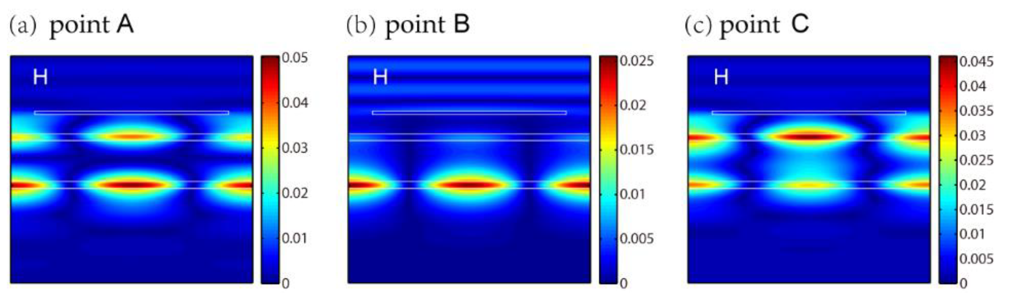
We start with reflection spectra of different thicknesses of layer 1, i.e., , as shown in Figure 2a. The parameters of the grating are set as , and . The thicknesses of layer 2, layer 3 and layer 4 are , and . The incident angle of is zero, indicating a normal incidence considered. Figure 1a shows the reflection spectra with different . It is found that the EIT-like effect gradually disappears as increases. By considering the symmetry and contrast of the result, we choose to illustrate the EIT-like effect in Figure 2b. The reflections with are also displayed as a comparison. The corresponding positions of these two parameters are also indicated as dashed lines in Figure 2a. Figure 2b clearly exhibits the EIT-like effect for in the red curve. The peak and dips of the EIT-like effect are marked as point A, B and C for simplicity. To reveal the physical mechanism, we analyze the EIT-like effect from two respects: detailed field distributions and theoretical results of equations. Figure 3 gives out the detailed magnetic field distributions of points A, B and C. The field distributions clarify that the EIT-like effect is formed by the destructive interference of the two waveguide resonances in layer 2 and layer 4. The peak of the EIT-like effect is induced by the waveguide resonance in layer 4 in Figure 3b. The simulated wavelength of the peak of EIT-like effect (i.e., point B in the red curve) is 720.8 nm. The theoretical wavelength of the peak of EIT-like effect is 720.0 nm, which is derived from the simultaneous Equations (3), (5) and (6) elaborated in the Structure and Theory section. The simulated wavelength of the peak of EIT-like effect is consistent with the theoretical wavelength (marked by the red line on the top of Figure 2b), demonstrating the origin of the EIT-like effect. For , there is no EIT-like effect, as shown in the black curve in Figure 1b, because the bright SPPs mode is too far to excite the waveguide resonances in layer 2 and layer 4. This proves that the EIT-like effect is a result of the coupling of two dark waveguide modes.
Then, we make an analogy of the EIT-like effect to the transition processes of an atom. The nanosystem without excitation is compared with the ground state of in an atom. The SPPs resonance, waveguide resonance in layer 2 and waveguide resonance in layer 4 are represented by the excited states of , and . When the propagating constant of the grating equals the wavenumber of SPPs, the SPPs resonance is excited by the incident wave, which corresponds to the transition process of . If the thickness of is proper, the waveguide resonance in layer 2 is excited by SPPs resonance, i.e., the process of . Therefore, the pathway of exciting waveguide resonance in layer 2 is . With proper , the waveguide resonance in layer 2 further excites waveguide resonance in layer 4 (this will be further explained in Figure 4b). Therefore, the pathway of exciting waveguide resonance in layer 4 is . To sum up, the EIT-like effect is formed by the destructive interference of the two pathways of and .
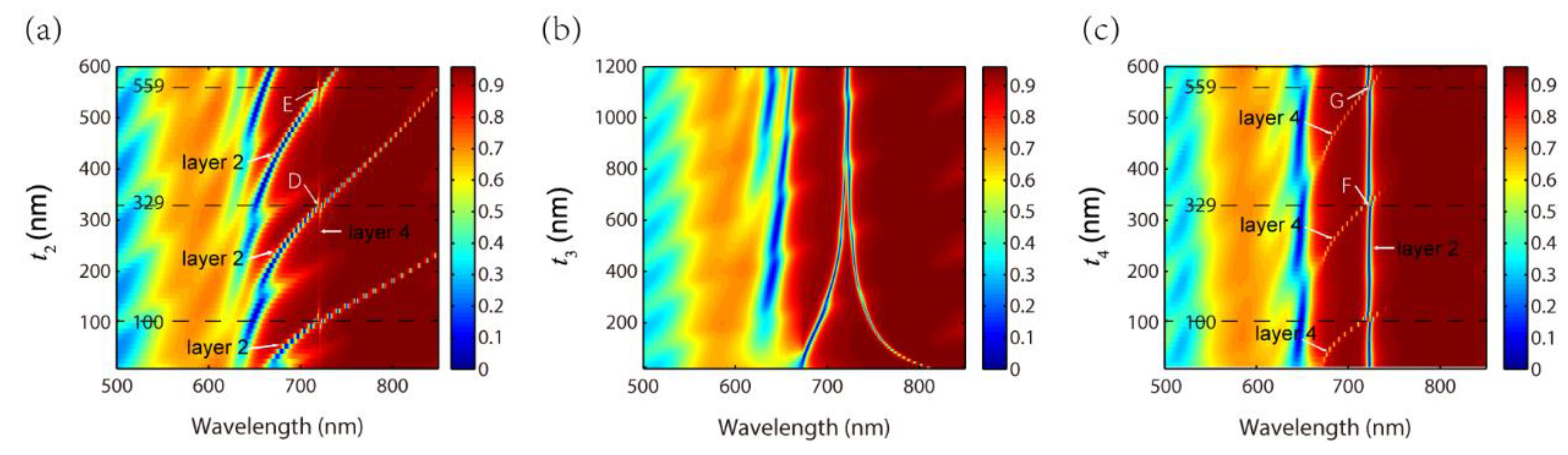
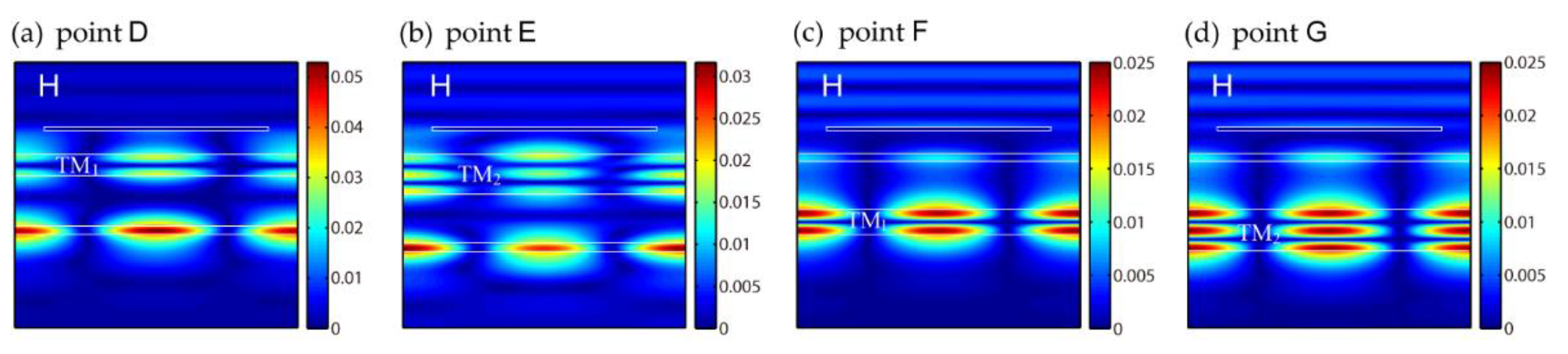
Subsequently, the influences of , and on the EIT-like effect are investigated, respectively, as shown in Figure 4. The basic parameters of , and are 100 nm, 640 nm and 100 nm. When one of the three changes, the other two remain unchanged. The other parameters are set as , , and . Figure 4a shows that the EIT-like effect appears repeatedly as increases due to higher orders of waveguide resonance in layer 2. The theoretical for higher orders of waveguide resonance of , and are 100 nm, 329 nm and 559 nm, which are derived from Equations (3), (4) and (6). The positions of of 100 nm, 329 nm and 559 nm are marked by black dashed lines in Figure 4a, which correspond to the calculated results. The dips of the EIT-like effect at and are marked as points D and E. The magnetic field distributions of points D and E are illustrated, respectively, in Figure 5a,b, which exhibit two maximums for and three maximums for along the y direction in layer 2. The magnetic field distribution of the dip of the EIT-like effect for at has already been shown in Figure 3a. Through the above analysis, the blue bands in Figure 4a stand for different orders of waveguide resonance in layer 2 and the unchanged narrow red line at 720.8 nm represents waveguide resonance in layer 4.
Figure 4b clearly demonstrates that the thickness of layer 3 (i.e., ) determines the bandwidth of the peak of EIT-like effect. As increases, the bandwidth of the peak decreases gradually. When , the EIT-like effect almost disappears because the two waveguide resonances cannot couple to each other for such a large distance between them. Therefore, only waveguide resonance in layer 2 remains in the spectrum. The explanation is supported by testing the field distribution at the dip of the reflection spectrum for (not shown in the paper).
Figure 4c shows the reflection spectra with different . Similarly, the EIT-like effect also appears repeatedly as increases because higher orders of waveguide resonance emerge in layer 4. Since we did not change , the wide blue line represents the unchanged waveguide resonance in layer 2. The theoretical for , and are the same as that of , i.e., 100 nm, 329 nm and 559 nm. The peaks of the EIT-like effect at and are marked as points F and G in Figure 4c. Figure 5c,d exhibit the magnetic field distributions of points F and G with and in layer 4.
In the previous discussions, we set for simplicity. Actually, the EIT-like effect is formed with for the same order as the waveguide modes in layer 2 and layer 4. We have also tested the reflection spectra of and . There is an EIT-like effect appearing in these two cases because resonant wavelengths of waveguide modes in layer 2 and layer 4 shift towards the same direction in the spectrum according to Equations (4) and (5). determines the bandwidth of the peak of EIT-like effect, so the choice of is not very strict. We set by considering the bandwidth and contrast of the EIT-like effect.
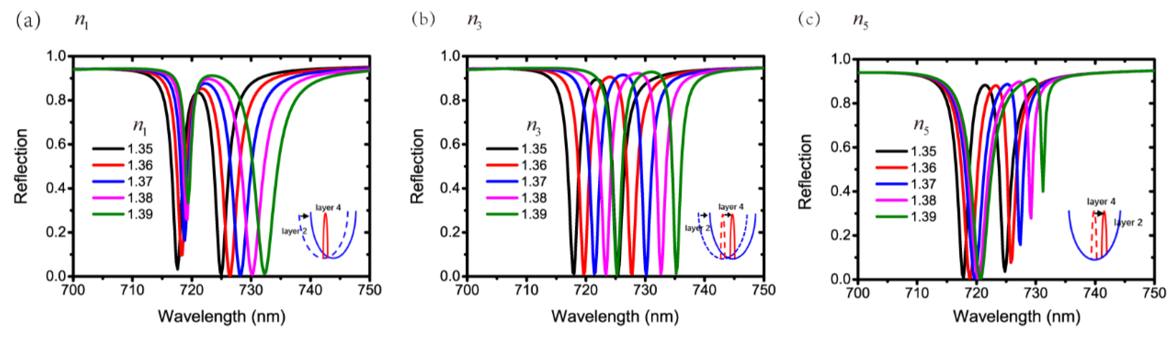
Next, we change the refractive indices of layer 1, layer 3 and the substrate. The structural parameters are , , , , , and . Figure 6a–c show the reflection spectra with different , and , respectively. It can be derived from Equations (4) and (5) that the increasing refractive index of the material next to the waveguide will lead to a redshift in the wavelength of the waveguide resonance. The simulation results in Figure 6a–c show the same redshift trend as , or increases. However, the phenomena are different. Particularly, the waveguide resonance in layer 2 redshifts with an increasing because layer 1 is adjacent to layer 2. Therefore, a redshifted waveguide resonance in layer 2 and an unchanged waveguide resonance in layer 4 form a Fano shape on the left falling edge in Figure 6a. Similarly, the waveguide resonance in layer 4 redshifts with an increasing because the substrate is next to layer 4. Consequently, a redshifted waveguide resonance in layer 4 and an unchanged waveguide resonance in layer 2 result in a Fano resonance on the right falling edge in Figure 6c. If we increase , the two waveguide resonances in layer 2 and layer 4 both redshift. Hence, the EIT-like effect still appears at a longer wavelength in Figure 6b. The schematic representations of the formation processes of Fano resonance and EIT-like effect with the increasing refractive indices are shown in the insets of Figure 6a–c.
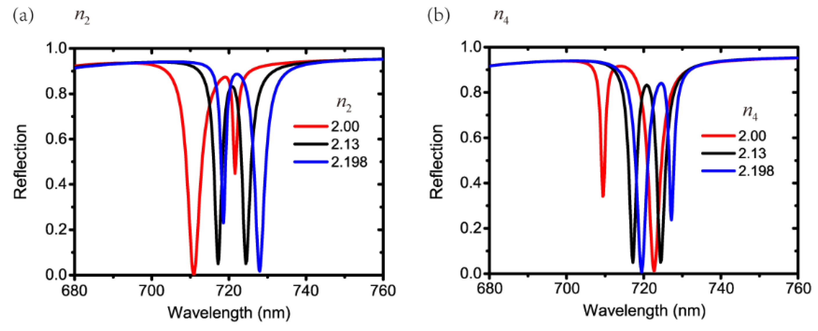
Afterwards, the influences of and on the EIT-like effect are investigated, as shown in Figure 7a,b. The refractive index of 2.13 denotes the TiO2 material employed in layer 2 and layer 4 in the previous discussions. Additionally, the refractive indices of 2.00 and 2.198 represent the material of Si3N4 and Ge-doped SiO2, respectively. Whether we increase or , the wavelength of the waveguide resonance in layer 2 or layer 4 redshifts according to Equations (4) and (5). The waveguide resonance in layer 2 redshifts with compared with that of . Therefore, a redshifted waveguide resonance in layer 2 and an unchanged waveguide resonance in layer 4 form a Fano resonance on the left falling edge, as seen in the blue curve in Figure 7a. For , the waveguide resonance in layer 4 redshifts compared with that of . A redshifted waveguide resonance in layer 4 and an unchanged waveguide resonance in layer 2 form a Fano resonance on the right falling edge, as seen in the blue curve in Figure 7b. Through the same way of analyzing, the simulated results with and can also be understood.
We further examine the grating parameters on the EIT-like effect. Figure 8a,b show the reflection spectra with different for and . The other parameters are , , , and . Compared with in Figure 1a, the EIT-like effect redshifts with an increasing . The reason of the redshift of the EIT-like effect is explained as follows. When the grating period of increases, the wavenumber of the SPPs resonance decreases according to Equations (2) and (3). The SPPs resonance excites the waveguide resonance, so the propagating constant of the waveguide resonance decreases. Through Equations (4) and (5), one can derive that the wavelengths of the two waveguide resonances redshift. Figure 8c illustrates the reflection spectra with a continuous change of for . It indicates that the peak of the EIT-like effect is broadening as increases.
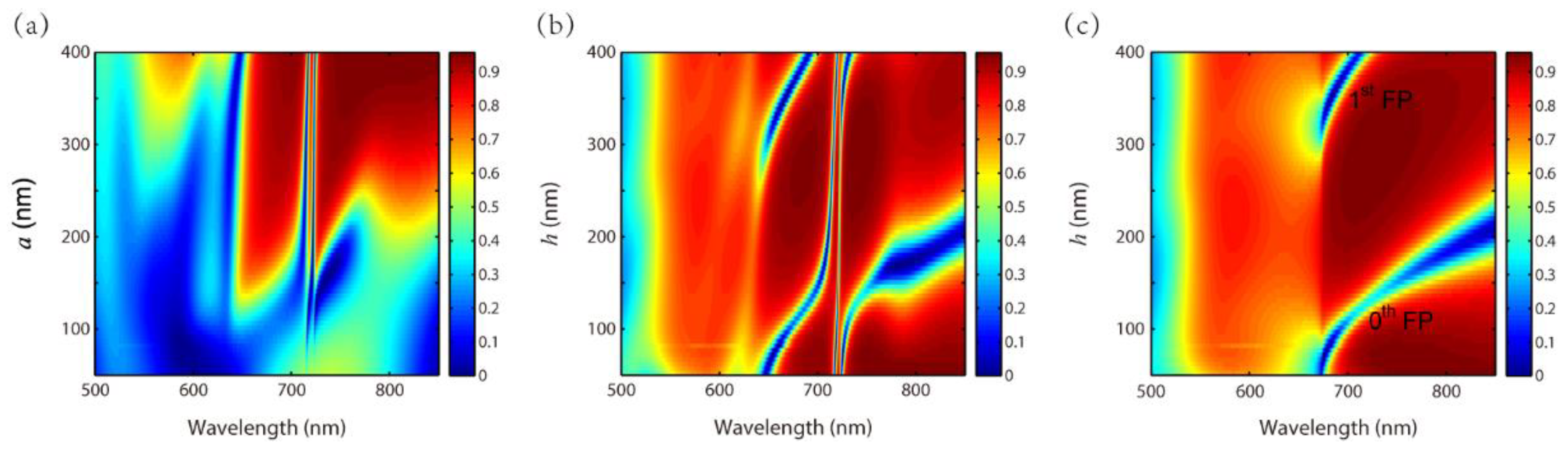
Figure 9a,b show reflection spectra with different grating widths and thicknesses . The other parameters are , , , and . Figure 9a exhibits that the EIT-like effect is not explicit for a small . This is due to the fact that the grating width is too small to sustain SPPs resonance. Therefore, the corresponding waveguide resonances in layer 2 and layer 4 are not excited. Figure 9b illustrates the evolution of the two waveguide resonances with an increasing . For comparison, we give out the reflection spectra with different of a nanosystem with Au grating and a fluoropolymer substrate in Figure 9c. As increases, only 0th and 1st orders of Fabry-Pérot (FP) resonance in the grating slit are indicated. In Figure 9b, the reflection spectra become complicated for 0th and 1st orders of FP resonance in the grating couple with the two waveguide resonances.
Finally, we make a summary of the EIT-like effect achieved in our proposed nanosystem and in other different nanosystems in Table 1. Zhang’s group introduced an EIT-like effect in plasmonic metamaterial by the coupling of bright dipole antenna and dark mode consisting of two parallel metal strips with a small separation [34]. Hu et al. reported an EIT-like effect with a bar resonator and two split SRRs [46]. Taubert et al. theoretically and experimentally demonstrated an EIT-like effect by the coupling of a broad bright dipolar to a narrow dark quadrupolar plasmon resonance [10]. Luo et al. achieved EIT-like effect in mid-infrared based on the strong coupling between localized and propagating plasmonic modes in layered graphene ribbon-grating and continuous sheet systems [47]. Vafapour et al. exhibited the EIT-like effect with two vertical bars as a bright plasmonic mode and a horizontal bar as a dark plasmonic mode [48]. Wei et al. reported the EIT-like effect due to the destructive interference between the bright and dark resonator of a dielectric metasurface consisting of two mutually perpendicular silicon-based nanoscale bars [49]. Zhang et al. presented the EIT-like effect in an MIM waveguide with a stub coupled ring resonator [50]. Wei et al. reported a tunable EIT-like effect in a graphene-based silicon–air grating structure [51]. He et al. realized the EIT-like effect based on the bright–bright mode coupling in a stacked metal-dielectric MM in the near-infrared regime [37]. Jin et al. studied the EIT-like effect at optical frequencies in a metasurface composed of two silver strips as two bright modes [52]. Fu et al. realized a tunable EIT-like effect in the mid-infrared region by using two parallel graphene nanostrips [38]. Our work is different from these previous reported nanosystems. The EIT-like effect in our proposed nanosystem is generated by two dark waveguide modes coupling at a visible regime.
4. Conclusions
In summary, we report an EIT-like effect with the coupling of two dark waveguide modes in the proposed nanosystem. The excitation of the EIT-like effect is demonstrated by simulated field distributions and theoretical equations. As the thickness of layer 2 or layer 4 increases, the EIT-like effect appears repeatedly due to the appearance of high orders of the component, i.e., and . The thickness of layer 3 determines the bandwidth of the peak of the EIT-like effect. An increase in any refractive index among , , and will result in a Fano resonance because of the coupling of a redshifted waveguide resonance and an unchanged waveguide resonance. When the refractive index of increases, the EIT-like effect still appears at a longer wavelength because both waveguide resonances redshift. We further examine the influence of grating parameters on the EIT-like effect. As the grating period of increases, the EIT-like effect redshifts and the bandwidth of its peak broadens. The EIT-like is not explicit for a small due to the fact that the grating width is too small to sustain SPPs. As the grating thickness of increases, the reflection spectra become complicated because the two waveguide resonances couple with 0th and 1st orders of FP resonance in the grating slit. Our work might stimulate more research on the EIT-like effect with two dark mode coupling.
Author Contributions
Conceptualization, Q.W. and W.P.; methodology, H.G.; validation, L.Y. and K.K.; formal analysis, S.C.; investigation, K.K.; data curation, H.G.; writing—original draft preparation, K.K.; writing—review and editing, Q.W.; supervision, W.P. All authors have read and agreed to the published version of the manuscript.
Funding
This research was funded by National Natural Science Foundation of China (NSFC), grant number 61520106013, 61727816 and 51661145025.
Data Availability Statement
The data presented in this study are available on request from the corresponding author.
Conflicts of Interest
The authors declare no conflict of interest.
References
- Boller, K.J.; Imamoglu, A.; Harris, S.E. Observation of electromagnetically induced transparency. Phys. Rev. Lett. 1991, 66, 2593–2596. [Google Scholar] [CrossRef] [PubMed] [Green Version]
- Yan, X.; Yang, M.; Zhang, Z.; Liang, L.; Wei, D.; Wang, M.; Zhang, M.; Wang, T.; Liu, L.; Xie, J.; et al. The terahertz electromagnetically induced transparency-like metamaterials for sensitive biosensors in the detection of cancer cells. Biosens. Bioelectron. 2019, 126, 485–492. [Google Scholar] [CrossRef]
- Wu, D.; Liu, Y.; Yu, L.; Yu, Z.; Chen, L.; Li, R.; Ma, R.; Liu, C.; Zhang, J.; Ye, H. Plasmonic metamaterial for electromagnetically induced transparency analogue and ultra-high figure of merit sensor. Sci. Rep. 2017, 7, 45210. [Google Scholar] [CrossRef] [PubMed] [Green Version]
- Liu, C.; Dutton, Z.; Behroozi, C.H.; Hau, L.V. Observation of coherent optical information storage in an atomic medium using halted light pulses. Nature 2001, 409, 490–493. [Google Scholar] [CrossRef] [Green Version]
- Kim, T.-T.; Kim, H.-D.; Zhao, R.; Oh, S.S.; Ha, T.; Chung, D.S.; Lee, Y.H.; Min, B.; Zhang, S. Electrically tunable slow light using graphene metamaterials. ACS Photonics 2018, 5, 1800–1807. [Google Scholar] [CrossRef] [Green Version]
- Safavi-Naeini, A.H.; Alegre, T.P.M.; Chan, J.; Eichenfield, M.; Winger, M.; Lin, Q.; Hill, J.T.; Chang, D.E.; Painter, O. Electromagnetically induced transparency and slow light with optomechanics. Nature 2011, 472, 69–73. [Google Scholar] [CrossRef] [PubMed] [Green Version]
- Sun, H.; Zhao, L.; Dai, J.; Liang, Y.; Guo, J.; Meng, H.; Liu, H.; Dai, Q.; Wei, Z. Broadband filter and adjustable extinction ratio modulator based on metal-graphene hybrid metamaterials. Nanomaterials 2020, 10, 1359. [Google Scholar] [CrossRef] [PubMed]
- Gu, J.; Singh, R.; Liu, X.; Zhang, X.; Ma, Y.; Zhang, S.; Maier, S.A.; Tian, Z.; Azad, A.K.; Chen, H.-T. Active control of electromagnetically induced transparency analogue in terahertz metamaterials. Nat. Commun. 2012, 3, 1151. [Google Scholar] [CrossRef] [Green Version]
- Hau, L.V.; Harris, S.E.; Dutton, Z.; Behroozi, C.H. Light speed reduction to 17 metres per second in an ultracold atomic gas. Nature 1999, 397, 594–598. [Google Scholar] [CrossRef]
- Taubert, R.; Hentschel, M.; Kaestel, J.; Giessen, H. Classical analog of electromagnetically induced absorption in plasmonics. Nano Lett. 2012, 12, 1367–1371. [Google Scholar] [CrossRef] [PubMed]
- Bai, Z.; Hang, C.; Huang, G. Classical analogs of double electromagnetically induced transparency. Opt. Commun. 2013, 291, 253–258. [Google Scholar] [CrossRef]
- Huang, Y.; Min, C.; Veronis, G. Subwavelength slow-light waveguides based on a plasmonic analogue of electromagnetically induced transparency. Appl. Phys. Lett. 2011, 99, 143117. [Google Scholar] [CrossRef] [Green Version]
- Tang, H.; Zhou, L.; Xie, J.; Lu, L.; Chen, J. Electromagnetically induced transparency in a silicon self-coupled optical waveguide. J. Lightwave Technol. 2018, 36, 2188–2195. [Google Scholar] [CrossRef]
- Yang, X.; Yu, M.; Kwong, D.-L.; Wong, C.W. All-optical analog to electromagnetically induced transparency in multiple coupled photonic crystal cavities. Phys. Rev. Lett. 2009, 102, 173902. [Google Scholar] [CrossRef] [PubMed] [Green Version]
- Hu, C.; Schulz, S.A.; Liles, A.A.; O’Faolain, L. Tunable optical buffer through an analogue to electromagnetically induced transparency in coupled photonic crystal cavities. ACS Photonics 2018, 5, 1827–1832. [Google Scholar] [CrossRef]
- Liu, N.; Langguth, L.; Weiss, T.; Kaestel, J.; Fleischhauer, M.; Pfau, T.; Giessen, H. Plasmonic analogue of electromagnetically induced transparency at the Drude damping limit. Nat. Mater. 2009, 8, 758–762. [Google Scholar] [CrossRef] [PubMed]
- Ma, Q.; Dai, J.; Luo, A.; Hong, W. Numerical and theoretical study of tunable plasmonically induced transparency effect based on bright-dark mode coupling in graphene metasurface. Nanomaterials 2020, 10, 232. [Google Scholar] [CrossRef] [Green Version]
- Ma, Q.; Zhan, Y.; Hong, W. Tunable metamaterial with gold and graphene split-ring resonators and plasmonically induced transparency. Nanomaterials 2019, 9, 7. [Google Scholar] [CrossRef] [Green Version]
- Sun, G.; Peng, S.; Zhang, X.; Zhu, Y. Switchable electromagnetically induced transparency with toroidal mode in a graphene-loaded all-dielectric metasurface. Nanomaterials 2020, 10, 1064. [Google Scholar] [CrossRef] [PubMed]
- Christofi, A.; Kawaguchi, Y.; Alu, A.; Khanikaev, A.B. Giant enhancement of Faraday rotation due to electromagnetically induced transparency in all-dielectric magneto-optical metasurfaces. Opt. Lett. 2018, 43, 1838–1841. [Google Scholar] [CrossRef]
- Zhang, L.; Tassin, P.; Koschny, T.; Kurter, C.; Anlage, S.M.; Soukoulis, C.M. Large group delay in a microwave metamaterial analog of electromagnetically induced transparency. Appl. Phys. Lett. 2010, 97, 241904. [Google Scholar] [CrossRef] [Green Version]
- Xiao, S.; Wang, T.; Liu, T.; Yan, X.; Li, Z.; Xu, C. Active modulation of electromagnetically induced transparency analogue in terahertz hybrid metal-graphene metamaterials. Carbon 2018, 126, 271–278. [Google Scholar] [CrossRef] [Green Version]
- Yin, X.; Feng, T.; Yip, S.; Liang, Z.; Hui, A.; Ho, J.C.; Li, J. Tailoring electromagnetically induced transparency for terahertz metamaterials: From diatomic to triatomic structural molecules. Appl. Phys. Lett. 2013, 103, 021115. [Google Scholar] [CrossRef] [Green Version]
- Xu, H.; Zhang, Z.; Wang, S.; Liu, Y.; Zhang, J.; Chen, D.; Ouyang, J.; Yang, J. Tunable graphene-based plasmon-induced transparency based on edge mode in the mid-infrared region. Nanomaterials 2019, 9, 448. [Google Scholar] [CrossRef] [PubMed] [Green Version]
- Zhang, J.; Xiao, S.; Jeppesen, C.; Kristensen, A.; Mortensen, N.A. Electromagnetically induced transparency in metamaterials at near-infrared frequency. Opt. Express 2010, 18, 17187–17192. [Google Scholar] [CrossRef] [PubMed] [Green Version]
- Hokari, R.; Kanamori, Y.; Hane, K. Comparison of electromagnetically induced transparency between silver, gold, and aluminum metamaterials at visible wavelengths. Opt. Express 2014, 22, 3526–3537. [Google Scholar] [CrossRef] [PubMed]
- Li, Q.; Liu, S.; Zhang, X.; Wang, S.; Chen, T. Electromagnetically induced transparency in terahertz metasurface composed of meanderline and U-shaped resonators. Opt. Express 2020, 28, 8792–8801. [Google Scholar] [CrossRef]
- Xiao, B.; Tong, S.; Fyffe, A.; Shi, Z. Tunable electromagnetically induced transparency based on graphene metamaterials. Opt. Express 2020, 28, 4048–4057. [Google Scholar] [CrossRef]
- Chen, M.; Xiao, Z.; Lu, X.; Lv, F.; Zhou, Y. Simulation of dynamically tunable and switchable electromagnetically induced transparency analogue based on metal-graphene hybrid metamaterial. Carbon 2020, 159, 273–282. [Google Scholar] [CrossRef]
- Yang, T.; Liu, X.; Zhou, J. Terahertz polarization conversion in an electromagnetically induced transparency (EIT)-like metamaterial. Ann. Phys. 2021, 533, 2000528. [Google Scholar] [CrossRef]
- He, X.; Huang, Y.; Yang, X.; Zhu, L.; Wu, F.; Jiang, J. Tunable electromagnetically induced transparency based on terahertz graphene metamaterial. RSC Adv. 2017, 7, 40321–40326. [Google Scholar] [CrossRef] [Green Version]
- Guo, Z.; Jiang, H.; Li, Y.; Chen, H.; Agarwal, G.S. Enhancement of electromagnetically induced transparency in metamaterials using long range coupling mediated by a hyperbolic material. Opt. Express 2018, 26, 627–641. [Google Scholar] [CrossRef] [Green Version]
- Han, Y.; Yang, J.; He, X.; Huang, J.; Zhang, J.; Chen, D.; Zhang, Z. High quality factor electromagnetically induced transparency-like effect in coupled guided-mode resonant systems. Opt. Express 2019, 27, 7712–7718. [Google Scholar] [CrossRef]
- Zhang, S.; Genov, D.A.; Wang, Y.; Liu, M.; Zhang, X. Plasmon-induced transparency in metamaterials. Phys. Rev. Lett. 2008, 101, 047401. [Google Scholar] [CrossRef] [PubMed] [Green Version]
- Chen, H.; Zhang, H.; Liu, M.; Zhao, Y.; Guo, X.; Zhang, Y. Realization of tunable plasmon-induced transparency by bright-bright mode coupling in Dirac semimetals. Opt. Mater. Express 2017, 7, 3397–3407. [Google Scholar] [CrossRef]
- Yahiaoui, R.; Burrow, J.A.; Mekonen, S.M.; Sarangan, A.; Mathews, J.; Agha, I.; Searles, T.A. Electromagnetically induced transparency control in terahertz metasurfaces based on bright-bright mode coupling. Phys. Rev. B 2018, 97, 155403. [Google Scholar] [CrossRef] [Green Version]
- He, F.; Han, B.; Li, X.; Lang, T.; Jing, X.; Hong, Z. Analogue of electromagnetically induced transparency with high-Q factor in metal-dielectric metamaterials based on bright-bright mode coupling. Opt. Express 2019, 27, 37590–37600. [Google Scholar] [CrossRef] [PubMed]
- Fu, G.-L.; Zhai, X.; Li, H.-J.; Xia, S.-X.; Wang, L.-L. Tunable plasmon-induced transparency based on bright-bright mode coupling between two parallel graphene nanostrips. Plasmonics 2016, 11, 1597–1602. [Google Scholar] [CrossRef]
- Pitchappa, P.; Manjappa, M.; Ho, C.P.; Singh, R.; Singh, N.; Lee, C. Active control of electromagnetically induced transparency with dual dark mode excitation pathways using MEMS based tri-atomic metamolecules. Appl. Phys. Lett. 2016, 109, 211103. [Google Scholar] [CrossRef]
- Hayashi, S.; Nesterenko, D.; Rahmouni, A.; Sekkat, Z. Observation of Fano line shapes arising from coupling between surface plasmon polariton and waveguide modes. Appl. Phys. Lett. 2016, 108, 051101. [Google Scholar] [CrossRef] [Green Version]
- Rodrigo, S.G.; Garcia-Vidal, F.J.; Martin-Moreno, L. Influence of material properties on extraordinary optical transmission through hole arrays. Phys. Rev. B 2008, 77, 075401. [Google Scholar] [CrossRef] [Green Version]
- Johnson, P.B.; Christy, R.W. Optical constants of the noble metals. Phys. Rev. B 1972, 6, 4370–4379. [Google Scholar] [CrossRef]
- Yee, K. Numerical solution of initial boundary value problems involving Maxwell’s equations in isotropic media. IEEE Trans. Antennas Propag. 1966, 14, 302–307. [Google Scholar]
- Maier, S.A. Plasmonics: Fundamentals and applications; Springer: New York, NY, USA, 2007; pp. 21–26. [Google Scholar]
- Kaplan, A.F.; Xu, T.; Guo, L.J. High efficiency resonance-based spectrum filters with tunable transmission bandwidth fabricated using nanoimprint lithography. Appl. Phys. Lett. 2011, 99, 143111. [Google Scholar] [CrossRef] [Green Version]
- Hu, J.; Lang, T.; Hong, Z.; Shen, C.; Shi, G. Comparison of electromagnetically induced transparency performance in metallic and all-dielectric metamaterials. J. Lightwave Technol. 2018, 36, 2083–2093. [Google Scholar] [CrossRef]
- Luo, W.; Cai, W.; Xiang, Y.; Wang, L.; Ren, M.; Zhang, X.; Xu, J. Flexible modulation of plasmon-induced transparency in a strongly coupled graphene grating-sheet system. Opt. Express 2016, 24, 5784–5793. [Google Scholar] [CrossRef]
- Vafapour, Z.; Alaei, H. Achieving a high Q-factor and tunable slow-light via classical electromagnetically induced transparency (Cl-EIT) in metamaterials. Plasmonics 2017, 12, 479–488. [Google Scholar] [CrossRef]
- Wei, Z.; Li, X.; Zhong, N.; Tan, X.; Zhang, X.; Liu, H.; Meng, H.; Liang, R. Analogue electromagnetically induced transparency based on low-loss metamaterial and its application in nanosensor and slow-light device. Plasmonics 2017, 12, 641–647. [Google Scholar] [CrossRef]
- Zhang, Z.D.; Wang, R.B.; Zhang, Z.Y.; Tang, J.; Zhang, W.D.; Xue, C.Y.; Yan, S.B. Electromagnetically induced transparency and refractive index sensing for a plasmonic waveguide with a stub coupled ring resonator. Plasmonics 2017, 12, 1007–1013. [Google Scholar] [CrossRef]
- Wei, B.; Liu, H.; Ren, G.; Yang, Y.; Ye, S.; Pei, L.; Jian, S. Graphene based silicon-air grating structure to realize electromagnetically-induced-transparency and slow light effect. Phys. Lett. A 2017, 381, 160–165. [Google Scholar] [CrossRef]
- Jin, X.-R.; Park, J.; Zheng, H.; Lee, S.; Lee, Y.; Rhee, J.Y.; Kim, K.W.; Cheong, H.S.; Jang, W.H. Highly-dispersive transparency at optical frequencies in planar metamaterials based on two-bright-mode coupling. Opt. Express 2011, 19, 21652–21657. [Google Scholar] [CrossRef] [PubMed]
Figure 1.
Schematic map of the proposed nanosystem: (a) Main view; (b) Side view.

Figure 2.
(a) Reflection spectra with different ; (b) Reflections with and .

Figure 3.
Magnetic field distributions of points (a) A, (b) B and (c) C in Figure 2b.
Figure 3.
Magnetic field distributions of points (a) A, (b) B and (c) C in Figure 2b.

Figure 4.
Reflection spectra with different (a) , (b) and (c) .

Figure 5.
Magnetic field distributions of points (a) D, (b) E, (c) F and (d) G in Figure 4a,c.
Figure 5.
Magnetic field distributions of points (a) D, (b) E, (c) F and (d) G in Figure 4a,c.

Figure 6.
Reflection spectra with different (a) , (b) and (c) .

Figure 7.
Reflection spectra with different (a) and (b) .

Figure 8.
Reflection spectra with different for (a) and (b) ; (c) Reflection spectra with different for .
Figure 8.
Reflection spectra with different for (a) and (b) ; (c) Reflection spectra with different for .

Figure 9.
Reflection spectra with different (a) and (b) of the proposed nanosystem; (c) Reflection spectra with different of a nanosystem with Au grating and a fluoropolymer substrate.
Figure 9.
Reflection spectra with different (a) and (b) of the proposed nanosystem; (c) Reflection spectra with different of a nanosystem with Au grating and a fluoropolymer substrate.


Table 1.
The summary of EIT-like effect in different nanosystems.
| Structure | Type | Coupling Manner | Frequency |
|---|---|---|---|
| Ag dipole antenna and two parallel Ag strips [34] | metasurface | bright-dark | near-infrared |
| One bar resonator and two split ring resonators [46] | metasurface | bright-dark | near-infrared |
| Au nano-cut-wire and quadrupole wire pair [10] | metamaterial | bright-dark | near-infrared |
| Graphene ribbon-grating/dielectric layer/graphene sheet [47] | metamaterial | bright-dark | mid-infrared |
| Three Ag bars [48] | metasurface | bright-dark | near-infrared |
| Two perpendicular Si-based nanoscale bars [49] | metasurface | bright–dark | near-infrared |
| MIM waveguide with stub coupled ring resonator [50] | metasurface | not mentioned | near-infrared |
| Graphene sheet/silicon–air grating/graphene sheet [51] | metamaterial | not mentioned | mid-infrared |
| Ag strip/SiO2 layer/Si rod [37] | metamaterial | bright-bright | near-infrared |
| Two Ag strips [52] | metasurface | bright-bright | visible |
| Two graphene strips [38] | metasurface | bright-bright | mid-infrared |
| Au grating and a multilayer structure | metamaterial | dark-dark | visible |
Publisher’s Note: MDPI stays neutral with regard to jurisdictional claims in published maps and institutional affiliations. |
© 2021 by the authors. Licensee MDPI, Basel, Switzerland. This article is an open access article distributed under the terms and conditions of the Creative Commons Attribution (CC BY) license (https://creativecommons.org/licenses/by/4.0/).
Share and Cite
MDPI and ACS Style
Wang, Q.; Kuang, K.; Gao, H.; Chu, S.; Yu, L.; Peng, W. Electromagnetically Induced Transparency-Like Effect by Dark-Dark Mode Coupling. Nanomaterials 2021, 11, 1350. https://0-doi-org.brum.beds.ac.uk/10.3390/nano11051350
AMA Style
Wang Q, Kuang K, Gao H, Chu S, Yu L, Peng W. Electromagnetically Induced Transparency-Like Effect by Dark-Dark Mode Coupling. Nanomaterials. 2021; 11(5):1350. https://0-doi-org.brum.beds.ac.uk/10.3390/nano11051350
Chicago/Turabian StyleWang, Qiao, Kaili Kuang, Huixuan Gao, Shuwen Chu, Li Yu, and Wei Peng. 2021. "Electromagnetically Induced Transparency-Like Effect by Dark-Dark Mode Coupling" Nanomaterials 11, no. 5: 1350. https://0-doi-org.brum.beds.ac.uk/10.3390/nano11051350
Note that from the first issue of 2016, this journal uses article numbers instead of page numbers. See further details here.