1. Introduction
Following the trend established by Moore’s Law, more transistors are being packed in a single chip as the dimensions continue to downscale. As of 2020, the transistor count is on the order of several tens of billions in CPU and GPU systems. This continuous miniaturisation makes the massive spread of electronic devices, computers, smartphones, and wearables possible, which is also followed by great manufacturing challenges, where conventional processes and materials are reaching their usability limits and thus requiring either an improvement or replacement. In this regard, copper interconnects, which act as electrical paths in integrated circuits, have also been downscaled, thereby experiencing a reduction in width and thickness. Yet, the process of metallisation of these copper interconnects requires a diffusion barrier layer on the sidewalls/bottoms of vias and lines to prevent Cu atoms from diffusing into the surrounding dielectrics. Currently, a TaN diffusion barrier layer and a Ta adhesion layer are employed to improve the bonding between Cu and TaN. Although Ta/TaN is effective as a diffusion barrier system, it increases the global interconnect resistivity as the miniaturisation progresses further, ultimately limiting the performance of the integrated circuits. Furthermore, Cu dewetting and electromigration—phenomena related to the adhesion strength between Cu and Ta [
1,
2]—are becoming more prominent, hence limiting the interconnect reliability [
3,
4]. In addition, Ta/TaN requires a Cu seed layer on top before the electrolytic deposition process is initiated in order to enable adequate via and line filling. Uniform Cu-seed/Ta/TaN layers have thus become increasingly more difficult to deposit over increasingly narrow vias using conventional fabrication techniques.
Alternative barrier layers have been considered to replace Ta/TaN, such as Ru- and Co-based binary systems—e.g., Ru-W, Ru-Mn, and Co-W [
5,
6,
7]. The Co-W system is an interesting candidate as a novel barrier material due to its electrical and thermal properties. Co exhibits a relatively low electrical resistivity in a wide range of thicknesses [
8,
9,
10], whereas W enhances the diffusion barrier properties [
11], preventing Cu from diffusing into the dielectrics. In [
11], it was shown that CVD-Co-W (with 20 at% W) displays equivalent diffusion barrier properties to PVD-TaN. Additionally, the interface adhesion strength in Cu/Co-W is higher than in Cu/Ta [
12,
13], favouring lower Cu diffusion along the interface Cu/barrier and subsequently improving the electromigration lifetime [
14]. From a manufacturing point of view, Co-W is an interesting alternative to Ta/TaN as well, because it can be synthesised by electrochemical routes that produce a high film uniformity and step coverage in narrow vias and lines. Additionally, Co-W can function as both a diffusion barrier and seed layer, whereupon Cu can be directly electroplated [
15]. Electroless methods used for the synthesis of Co-W-based thin films have been reported in the literature [
16,
17,
18], but the direct electroplating of Cu on Co-W-based thin films is frankly unaddressed. The feasibility of Co-W as a directly electroplatable diffusion barrier layer to interconnect metallisation depends on its capability to grow a Cu film on top, with adequate morphological and microstructural characteristics and equivalent or superior electronic performance to conventional barrier layer systems. This work proposes a method for Cu electrocrystallisation on top of Co-W thin films using conventional acidic electroplating baths, focusing on the initial stages of Cu film formation.
2. Experimental
2.1. Co-W Thin Film Deposition
A ≈ 100 nm layer of SiO2 was deposited on top of a p-type boron-doped Si (100) wafer (Silicon Valley Microelectronics, Santa Clara, CA, USA) by plasma-enhanced chemical vapour deposition (PECVD) with a high radio frequency in a CVD MPX chamber (SPTS Technologies Ltd., Newport, UK). The wafer was diced into 15 mm × 15 mm substrates, whereupon Co-W films were deposited by DC magnetron sputtering in a confocal ultra-high vacuum sputtering system (Kenosistec, Binasco, Italy). Co and W were simultaneously sputtered from their respective targets (99.95%, Testbourne Ltd., Basingstoke, UK) for 600 s. Films with different W contents were deposited by applying a power bias between 40 and 100 W on the W target while keeping the Co target fixed at 40 W. The base and working pressures were 6.4 × 10⁻⁵ and 6.9 × 10⁻¹ Pa, respectively, maintaining an Ar flux of 20 sccm into the sputtering chamber. Co-W film thickness was measured using a contact profilometry instrument (KLA-Tencor, Milpitas, CA, USA).
2.2. Cu Electroplating
Cu was directly electroplated on Co-W/SiO2/Si substrates using an acidic electrolyte of 0.05 M CuSO4∙5H2O (99.995%, Sigma-Aldrich, St. Louis, MO, USA), 0.05 M H2SO4 (Honeywell/Fluka, Charlotte, NC, USA), 1 mM NaCl (Honeywell/Fluka, Charlotte, NC, USA), and 300 ppm polyethylene glycol (PEG) 600 (Fluka Chemie GmbH, Buchs, Switzerland) in double-distilled water. Electrolyte acidity was measured with a FiveEasy™ F20 digital pH meter (Mettler Toledo, Greifensee, Switzerland). Galvanostatic direct current (DC) and pulsed current (PC) plating routines were employed using a Gamry potentiostat/galvanostat Interface 1000E (Gamry Instruments, Warminster, PA, USA) with a simple two-electrode cell configuration, removing the need for the use of reference electrodes. The plating was carried out at room temperature in a 200 cm3 poly(methyl methacrylate) container without electrolyte stirring using a >99.9% pure Cu coil as the counter-electrode (anode) fixed at a ≈15 mm distance from the substrate (cathode). Prior to each plating routine, the substrates were pre-treated in a 1:20 H2SO4 solution for 60 s to remove possible oxidation present on the Co-W film surface, followed by rinsing in double-distilled water for another 60 s, both under ultrasonic agitation. The substrates were then dried by Ar blowing and masked with a polymeric film, limiting the exposed area to a circle of 0.20 cm2. After deposition, substrates were immediately removed from the electrolyte, rinsed in double-distilled water, and dried with soft Ar blowing.
2.3. Structural and Chemical Characterisation of Substrate and Cu Films
The as-sputtered Co-W film surfaces were observed by scanning electron microscopy, SEM (Thermo Fisher Scientific Quanta 400FEG ESEM, Thermo Fisher Scientific, Hillsboro, OR, USA), and their composition was estimated by energy-dispersive X-ray spectroscopy, EDS (EDAX Genesis X4M, AMETEK, Berwyn, PA, USA). The compositional analysis was complemented by X-ray photoelectron spectroscopy, XPS (ESCALAB™ 250 Xi, Thermo Fisher Scientific, Waltham, MA, USA), and the film structure was determined by grazing incidence X-ray diffraction (GIXRD) at an angle of 1.5° using Cu Kα radiation (λ = 1.54060 Å) and a step size of 0.02 °·s−1. The surfaces of the Cu/Co-W films were also observed by SEM and optical microscopy (Leica DM4000 M, Leica Microsystems GmbH, Wetzlar, Germany), where the substrate–film interface cross-section was prepared by focused ion-beam milling (Thermo Fisher Scientific Helios 450S, Thermo Fisher Scientific, Waltham, MA, USA). Surface roughness changes in response to the chemical pre-treatment were measured by atomic force microscopy, AFM (Veeco Metrology Multimode, Veeco Instruments Inc., Oyster Bay, NY, USA), with a Bruker TESPA-V2 tip. Quantitative image analysis was employed on SEM images using the ImageJ software version 1.51p, National Institutes of Health, Bethesda, MD, USA.
3. Results and Discussion
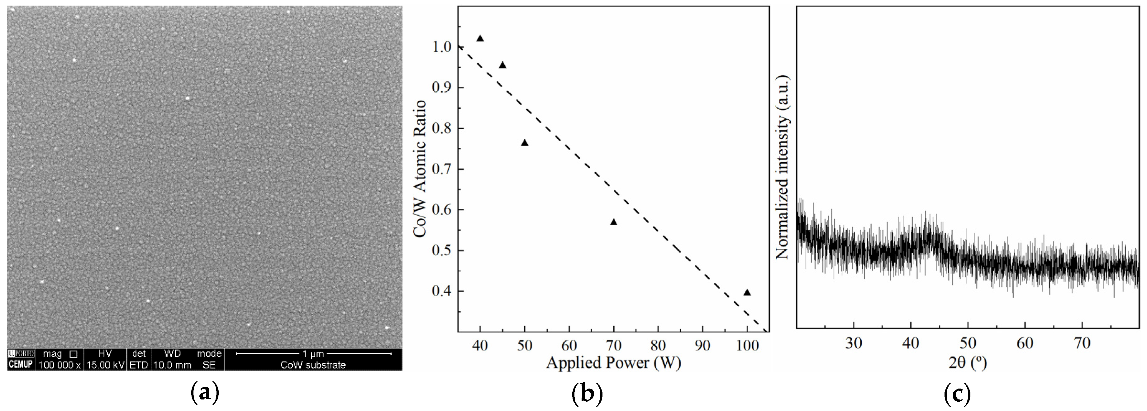
The sputtering conditions required to produce Co-W thin films with the desired chemical compositions were first investigated. As mentioned above, the power applied to the Co target was fixed at 40 W, while the one applied to the W target varied between 40 and 100 W. Sputtered films with 25 nm in thickness (measured by contact profilometry) display a uniform smooth surface (
Figure 1a). Estimating the chemical composition of such Co-W thin films using EDS at 15 keV requires special attention due to the large interaction volume, in the range of micrometres, picking up a strong X-ray signal from the SiO
2/Si underneath. EDS spectra were obtained with a 15 keV electron beam to excite Co K and W L spectral lines, which do not overlap with Si and O emission lines, and were used for elemental semi-quantification after 200 s of acquisition time to improve the signal-to-noise ratio. Higher Co/W atomic ratios were obtained as the power on the W target decreased (
Figure 1b), but due to the inherent limitations mentioned before, these values should be considered more as a qualitative assessment. Co-W films near equimolar composition were selected in this work for subsequent Cu electrodeposition. Su et al. [
15] demonstrated that equimolar Co-W films display the best plating behaviour while being effective as a diffusion barrier. GIXRD confirms the amorphous structure of the film, allowing it to adequately function as a diffusion barrier layer (
Figure 1c).
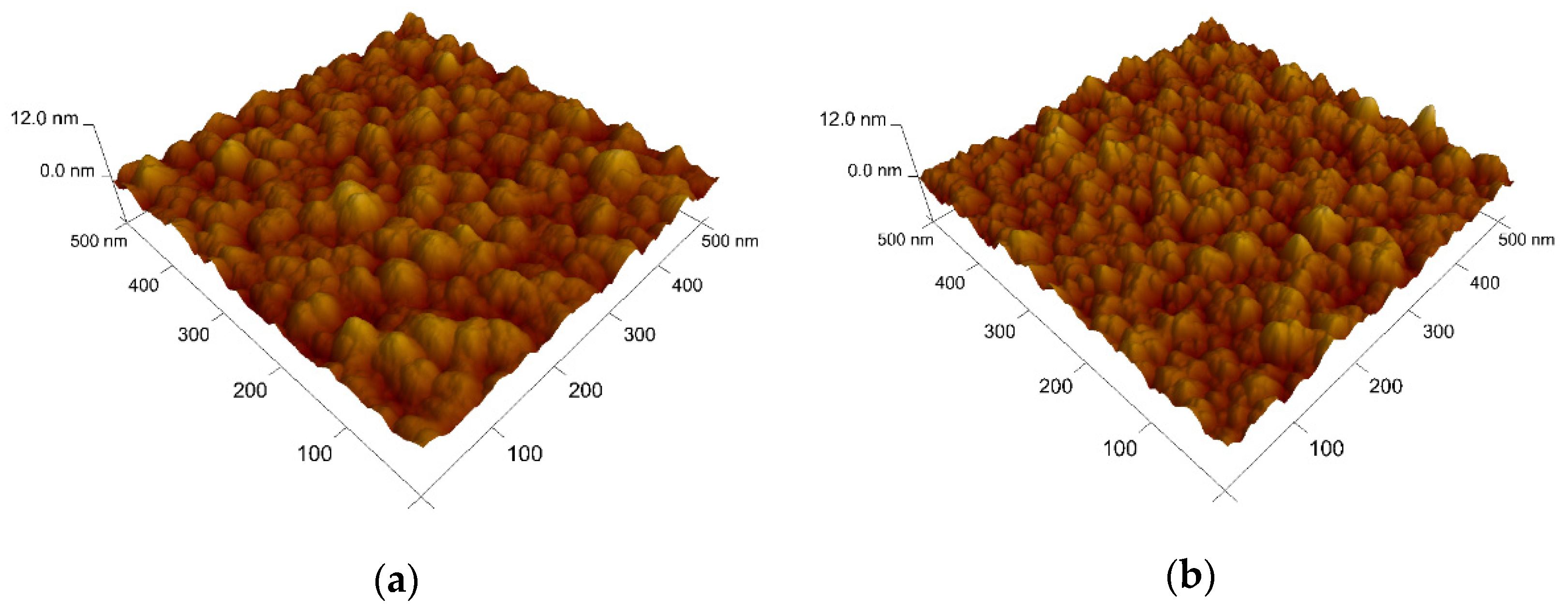
The effect of the sulphuric acid pre-treatment before electroplating was evaluated by AFM in tapping mode. By comparison fo the images in
Figure 2, it can be seen that the pre-treatment etched the surface, leaving a slightly more sharpened profile. The average surface roughness (
Sa) of a 500 nm × 500 nm area was determined to be 1.01 nm for the untreated surface, and 1.05 nm after pre-treatment, using the
NanoScope software 6.13R1 (Veeco Instruments Inc., Oyster Bay, NY, USA). Cu electrodeposition was conducted under a strict procedure to reduce the contact time between the substrate and the electrolyte to the minimum necessary for deposition, and to ensure maximum reproducibility between plating events. A comparison of the results of different plating conditions was undertaken using the central regions of the films. PC electrodeposition was employed as an alternative to DC for its added capability to not only control the applied current density, but also its on (
ton) and off (
toff) times. PC Cu films have been reported to display better electrical, thermal, and mechanical properties when compared to its DC counterparts [
19,
20,
21]. A comparison between PC and DC electrodeposition modes can also provide further insight into the Cu nucleation and growth on Co-W thin films.
To isolate the effect of pulsed current density,
jp, on Cu nucleation and growth, deposition times were decreased from 208 to 26 s with an increase in
jp from 5 to 40 mA·cm
−2, maintaining the total electrical charge supplied to the substrate unchanged. According to expression (1),
where
Q is the total charge supplied in C,
η the duty cycle given by Equation (2) and
t the total deposition time in s.
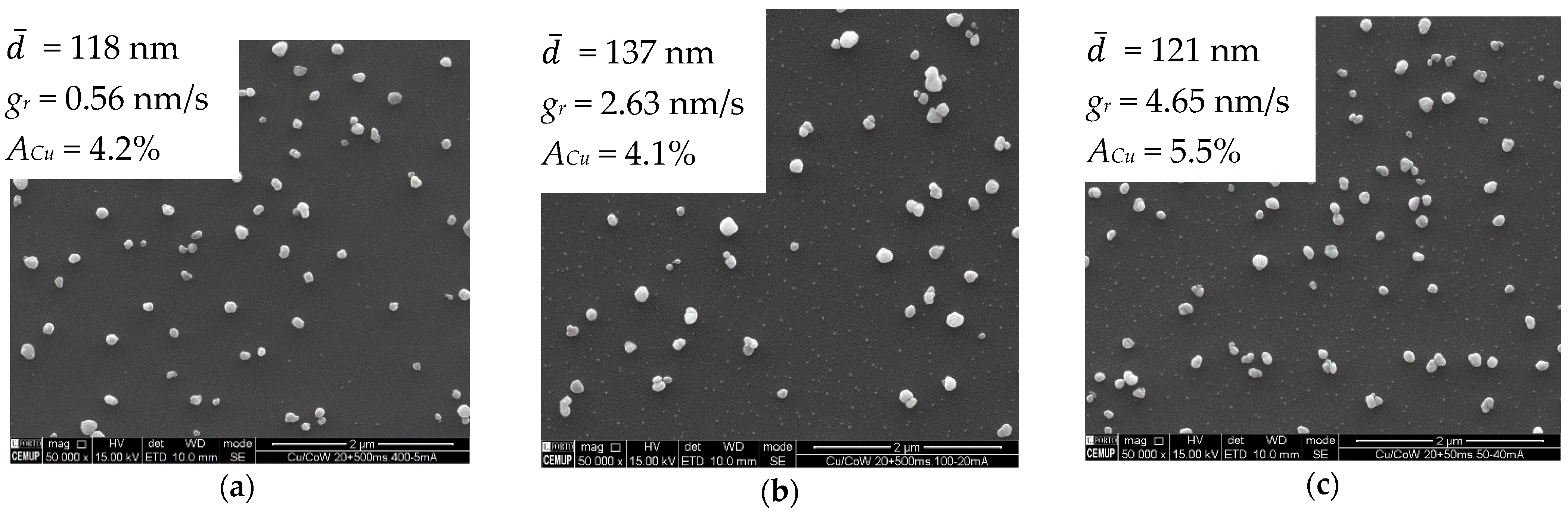
The Cu particles form on Co-W by instantaneous nucleation, whereby the nuclei density is higher when
jp rises to 20 mA·cm
−2 (
Figure 3). The number of active sites for nucleation reaches saturation around this current density, since it does not increase for higher
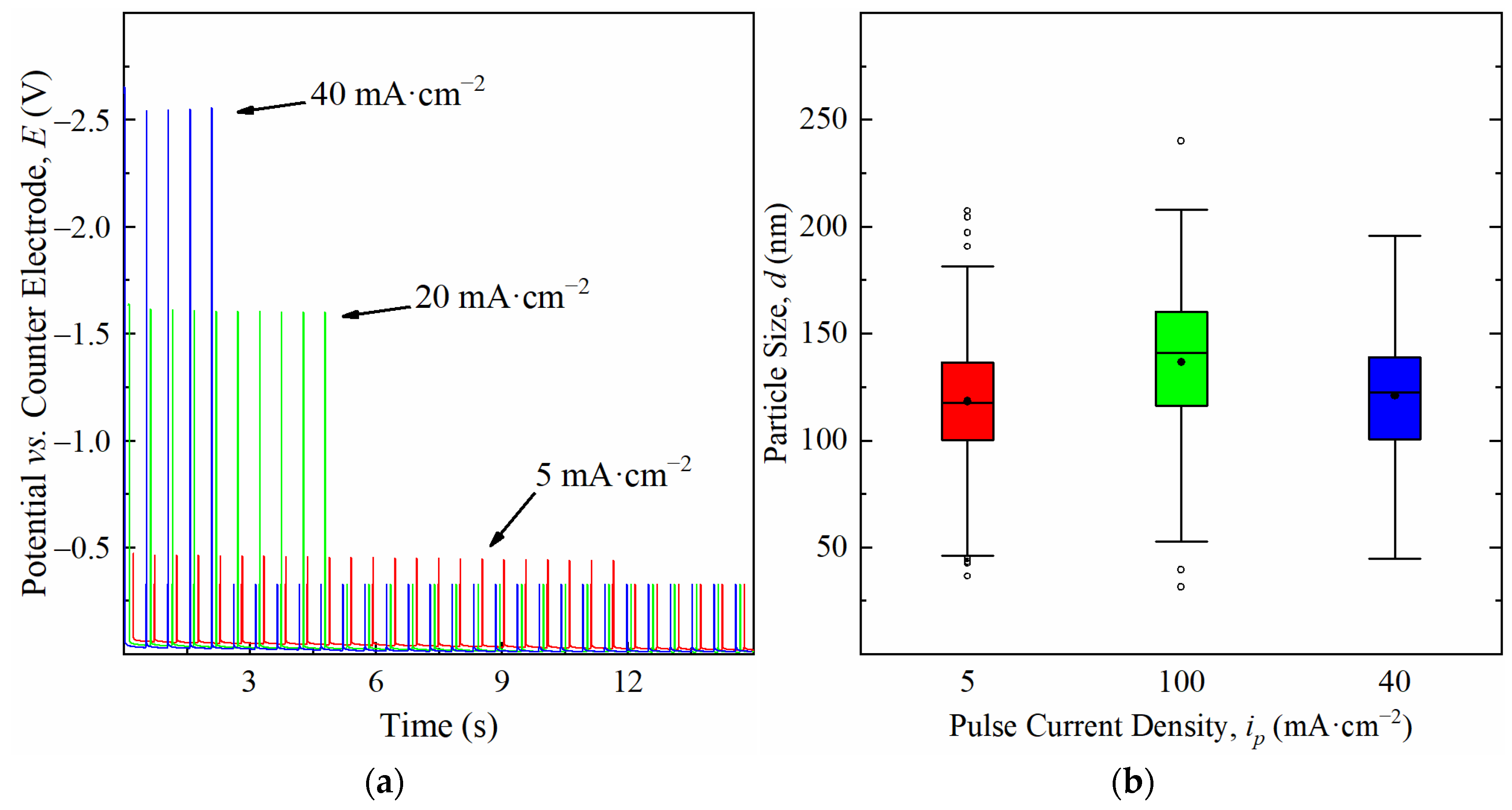
jp. Nucleation seems to occur during the first pulses of current, followed by nuclei growth, as soon as it becomes more energetically favourable, as indicated by the drop in cathodic potentials seen in the chronopotentiometric curves obtained for each deposition (
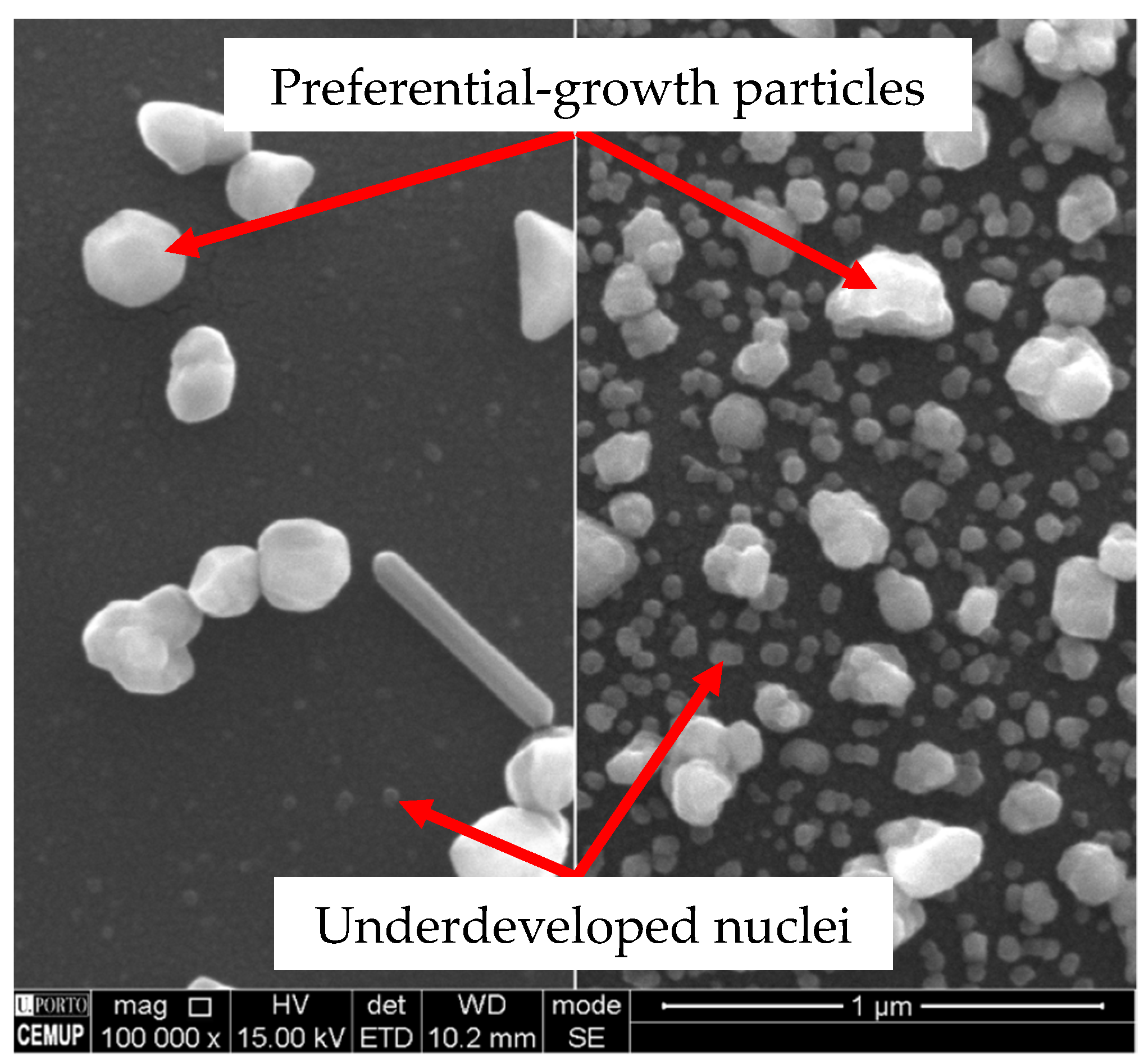
Figure 4a). Only a relatively small number of nuclei grow, whereas the remaining preserve what appears to be an embryonic-state, with sizes of less than 20 nm, resulting in a bimodal particle size distribution. It is noteworthy that the number of growing particles is approximately the same, regardless of
jp. PC deposition is reported to promote a faster growth of specific crystallographic orientations [
22,
23], which could in part explain the preferential growth of a few nuclei, due to their more favourable orientation. However, this does not explain why the number of growing particles at 20 mA·cm
−2 is near the same as the one observed at 5 mA·cm
−2. Such an effect results in particles reaching a similar average size and identical distribution profiles regardless of nuclei density (
Figure 4b). This indicates that higher current densities increase particle growth rates but fail to promote better substrate coverage, which was confirmed by measuring the substrate area occupied by Cu particles,
ACu. The growth rate,
gr, refers to the average velocity of 2D expansion of the particles given by Equation (3), where
Δ is the increase in average particle size and
Δt the time required for growth. Values of
represent particle diameter and were determined from the 2D projected area,
, on the substrate according to Equation (4). A minimum of 200 coarse particles were measured per condition. Very small particles were not considered in the calculation of
.
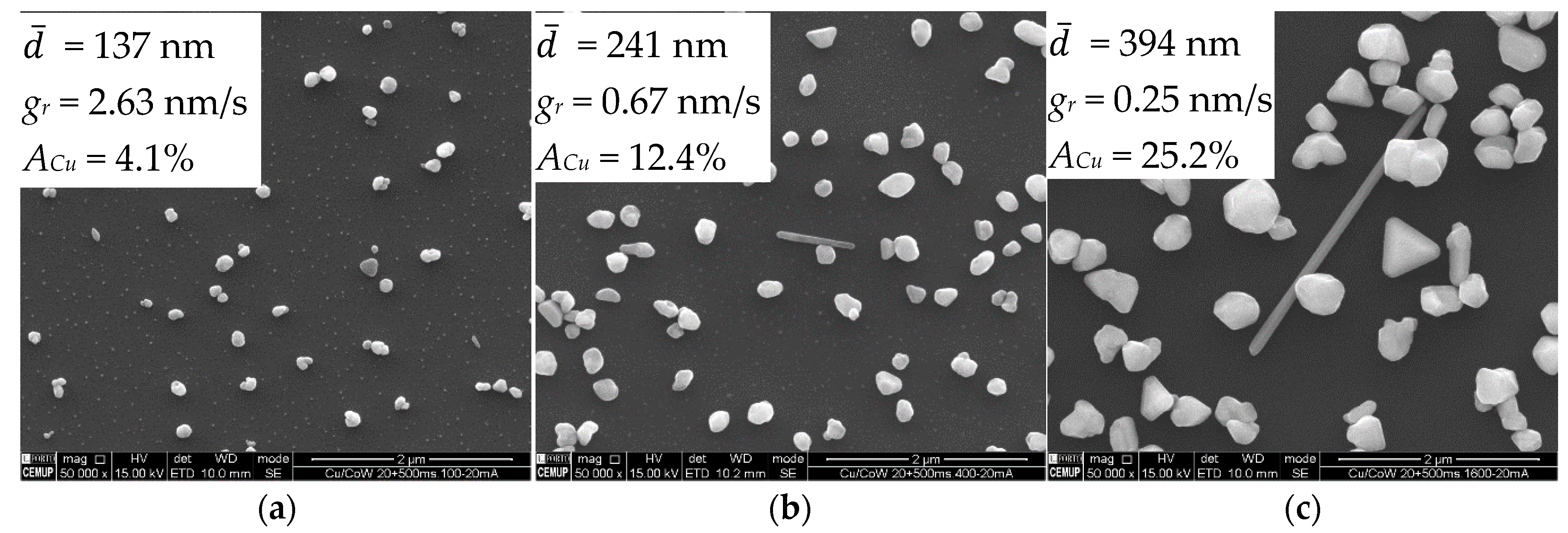
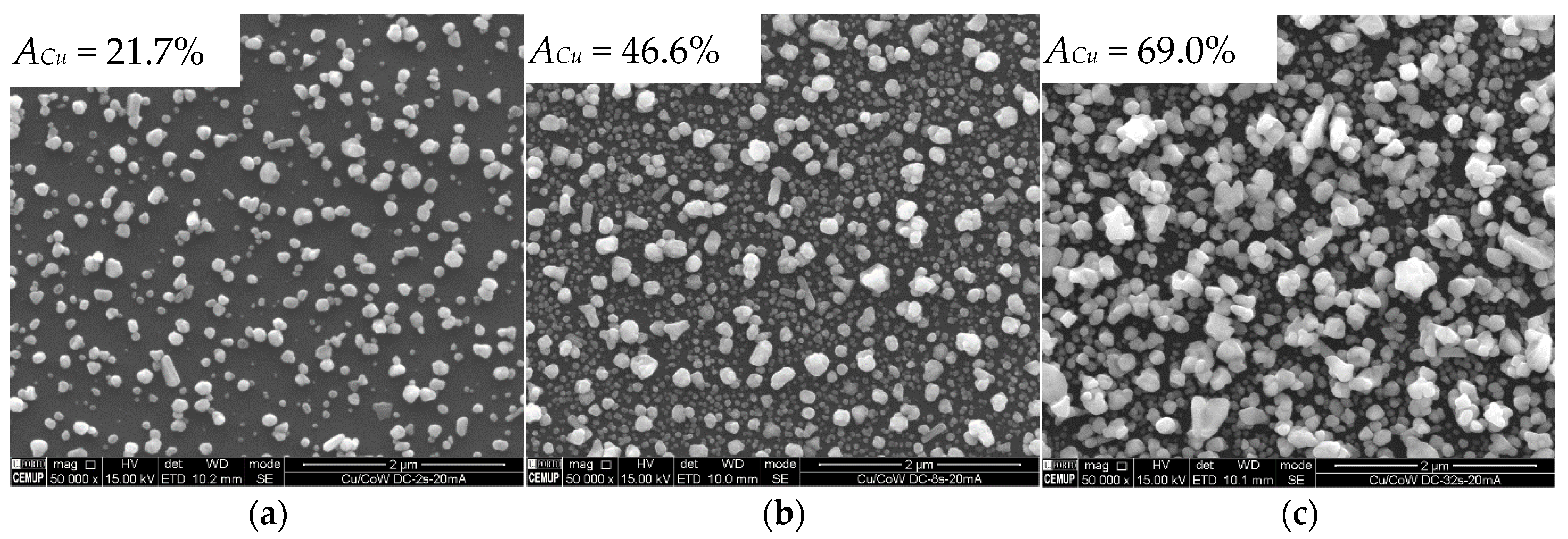
Longer deposition times (at constant
jp) promote further growth at lower rates (
Figure 5). Particles increase in volume through a preferential crystallographic growth mechanism, leading to more polygonal/faceted shapes (
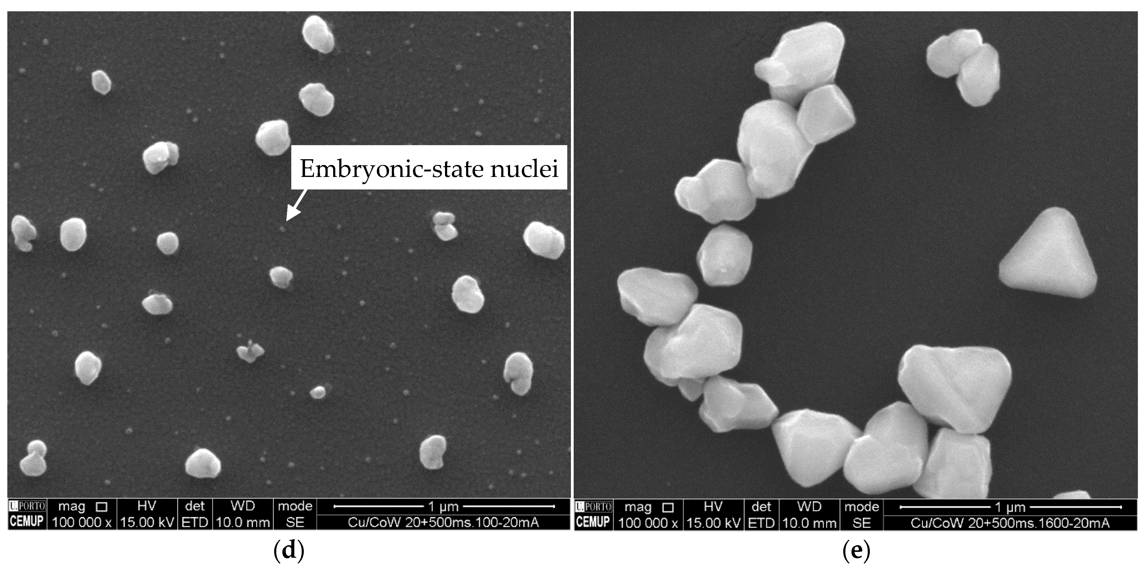
Figure 5a–c). The embryonic-state nuclei that did not grow after 52 s of deposition (
Figure 5d), remained mostly unaltered after 208 s, becoming undetectable in SEM imaging after 832 s (
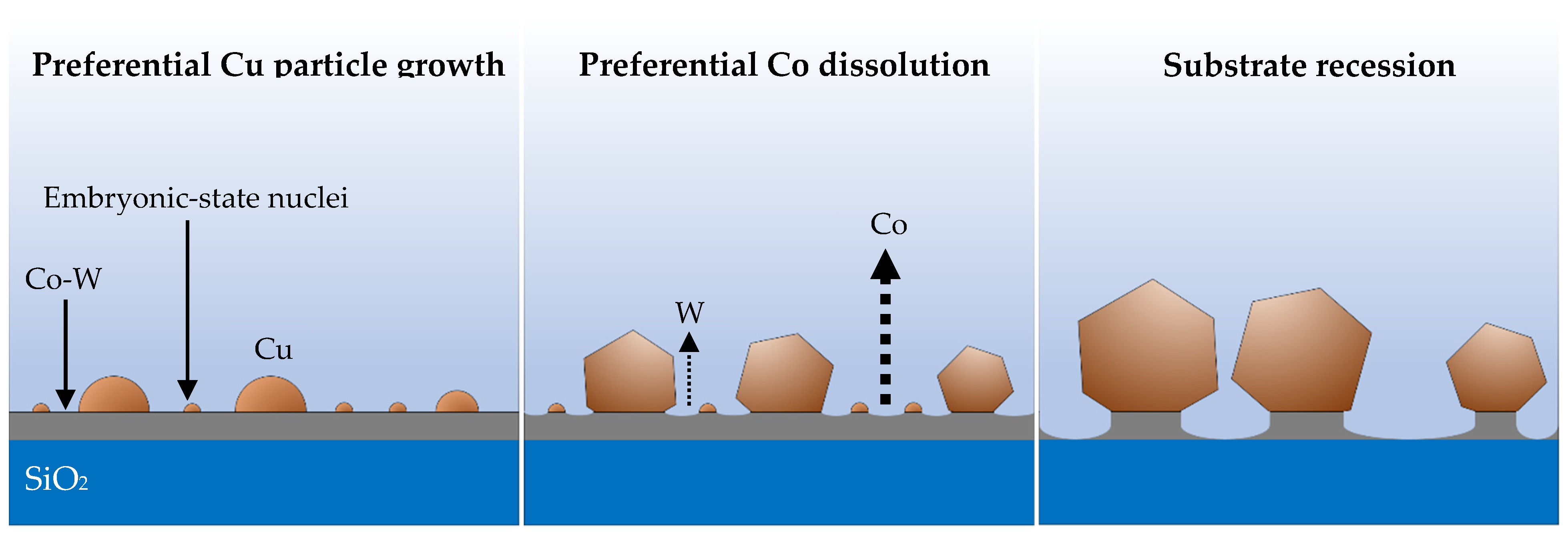
Figure 5e). These nuclei disappear either by direct dissolution into the electrolyte or by dissolution of the substrate underneath them. The acidic nature of the electrolyte herein used (pH ≈ 1.8) can dissolve Cu but is particularly aggressive to the Co-W substrate [
15,
24]. The nucleation and growth mechanism for Cu and the effects of the substrate dissolution are illustrated in
Figure 6.
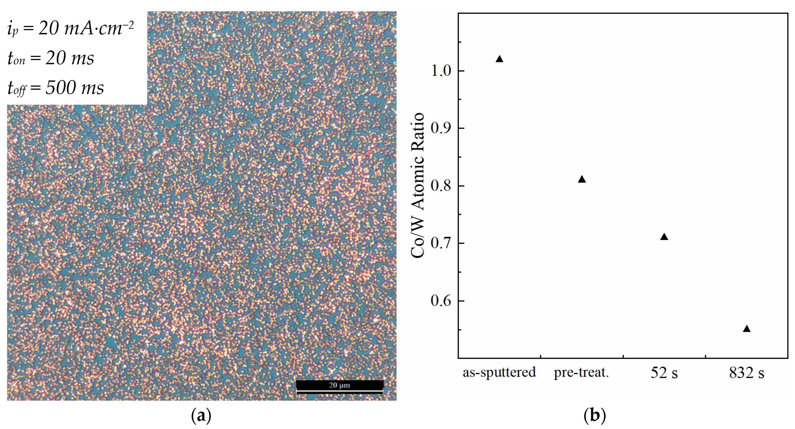
The incorporation of W in the Co film reduces the substrate dissolution rate but does not prevent it. After 832 s of deposition, the SiO
2 layer becomes visible in optical microscopy, confirming the dissolution/recession of the Co-W substrate (
Figure 7a). EDS analysis reveals a decrease in the Co/W atomic ratio with increasing immersion times (
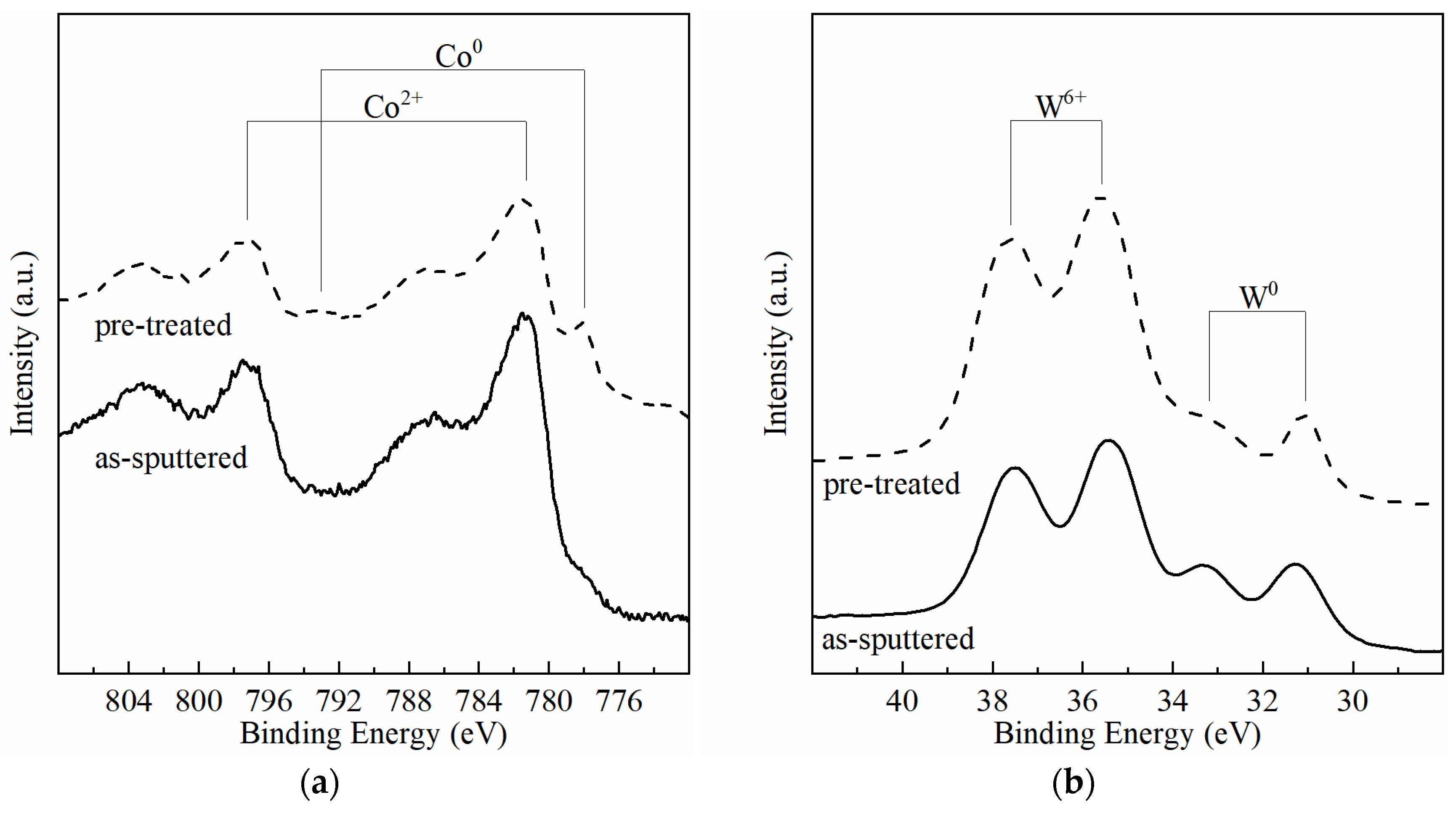
Figure 7b), indicating that substrate recession is mediated by a quicker dissolution of Co. XPS analysis detects the presence of W and Co in both metallic and oxidised form, before and after pre-treatment (
Figure 8). The peaks at 781 and 797 eV correspond to Co
2+, whereas the peaks at 793 and 778 eV correspond to metallic Co; the peaks at 37.5 and 35.3 eV correspond to W
6+, whereas 33.2 and 31.2 represent metallic W [
25]. After acidic pre-treatment, the relative intensity of Co peaks decreases, whereas W peaks increase, confirming that exposure of the substrate to acidic solution dissolves Co quicker than W.
After 2 s of DC deposition, the nuclei density seems equivalent to that observed in PC after 52 s, which comprises the same amount of transferred charge according to Equation (1) (for DC,
η = 1). The nuclei continue to increase in number and in size up to 8 s (DC), contrasting with what happens in PC for equivalent
Q, where the number of nuclei and growing particles remain practically unchanged (
Figure 9). The off time between pulses in PC deposition enhances the preferential growth of a few nuclei, resulting in a strong bimodal particle size (
Figure 10). During
toff, the current measured in the instrument is negligible and the corresponding cathodic potential applied is in the order of only a few mV. The dissolution rate is, thus, likely to be higher during
toff than during
ton, which may be controlling nuclei density by the dissolution of the less attached Cu particles or by dissolving the Co-W substrate directly underneath them. Another possible explanation for a lower nuclei density in PC deposition is that the number of active sites for nucleation decreases with the immersion time. It has been reported that the number of electrodeposited Cu nuclei decreases with increasing W content in Co-W and Ru-W substrates [
15,
26]. Accordingly, in this case, the selective dissolution of Co leads to substrate enrichment in W, rendering it difficult to nucleate further as the immersion time increases. In DC, there is no interval time and the total amount of charge is transferred continuously within only a few seconds. The average current density,
J, which can be calculated dividing Equation (1) by
t, is much higher in DC,
J = 20 mA·cm
−2, than in PC,
J = 0.77 mA·cm
−2. A similar
J value was reported using a similar electrolyte in DC mode (1 mA·cm
−2) [
15], resulting in incomplete substrate coverage, similar to
Figure 5a, suggesting that higher values of
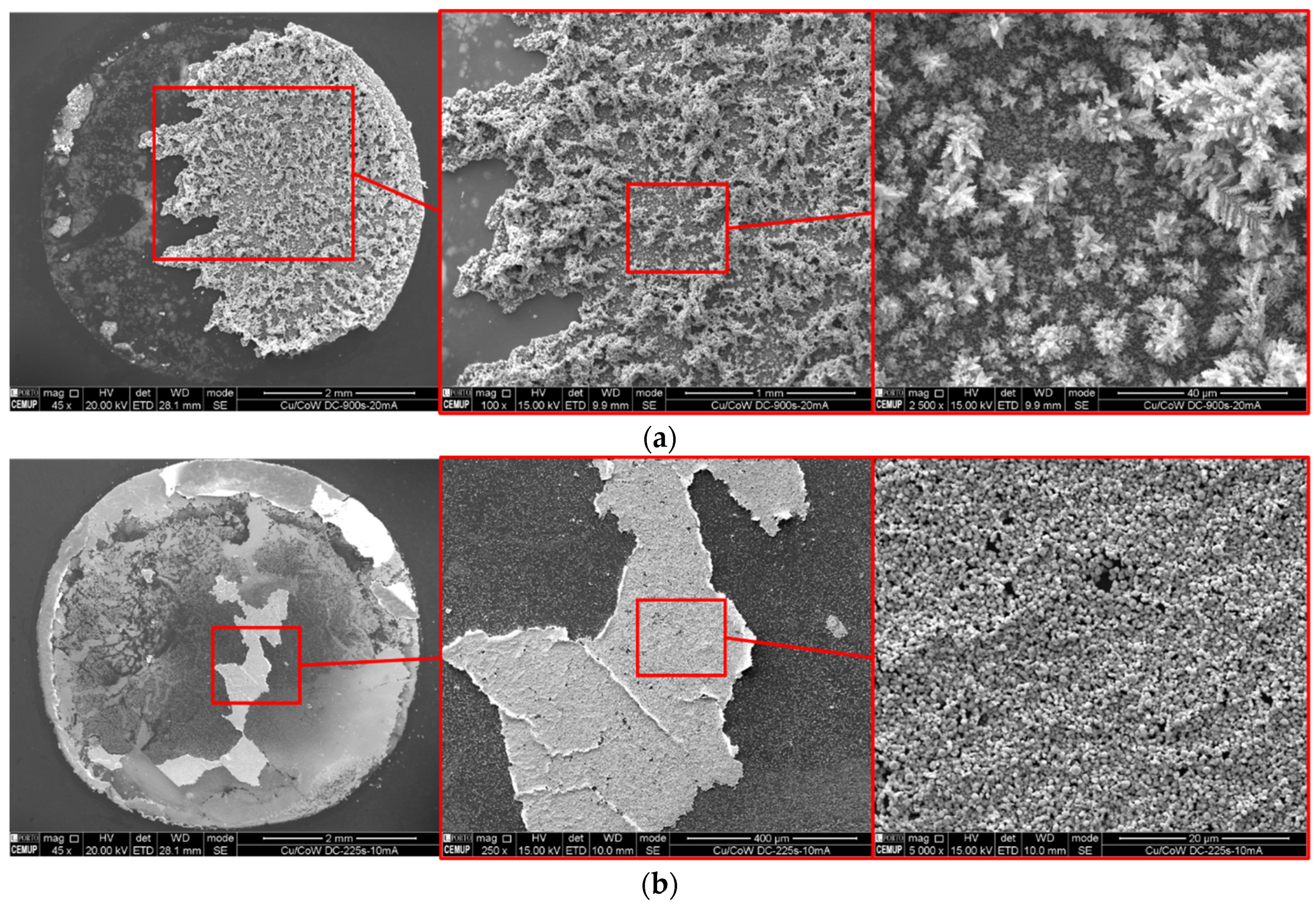
J are required to achieve better substrate coverage. Exposure time to the electrolyte is also substantially shorter in DC than in PC for the same transferred charge, reducing the extent of nuclei and substrate dissolution. Therefore, DC facilitates a denser nucleation and weakens the development of preferential orientation, leading to a more uniform growth of the nuclei (
Figure 11). Longer DC deposition times of up to 32 s do not seem to increase the nuclei density but result mainly in particle growth, especially in the direction perpendicular to the substrate. Although substrate coverage improves, the method used for measuring this coverage fails to give an accurate result in this particular case. Higher values of
ACu obtained after 32 s of DC deposition are largely due to the protuberant particles that grow outwards and overlap the substrate, without effectively covering it. These substrate areas left uncovered will eventually undergo complete dissolution, whereas further particle growth will result in a discontinuous branched-like structure, mechanically inconsistent and poorly adhered to the substrate, as can be seen after 900 s of deposition in
Figure 11a. Lowering the current density to 10 mA·cm
−2 yields a similar result after 225 s of deposition. Although handled with care, these films are easily torn apart after deposition during rinsing and drying. The film consists of a discontinuous aggregate of Cu particles that detaches from the substrate (
Figure 11b).
A method that could quickly coat the substrate with Cu is required to isolate the Co-W layer from the electrolyte and prevent its dissolution, which cannot be achieved by simply increasing the current density, since hydrogen reduction at the solid–liquid interface becomes a major problem, even with stirring. Although hydrogen bubbling was not observed during the first few seconds of deposition even at current densities higher than 5 mA·cm
−2, for longer times small bubbles were seen forming at the border of the substrate, reducing the overall deposition efficiency. Alternatively, a decrease in substrate dissolution rate would likely allow a higher nucleation and a more uniform particle growth, resulting in improved substrate coverage. Therefore, we prepared a less aggressive version of the electrolyte by pouring a portion of the original electrolyte (pH 1.8) in a beaker, progressively adding a few drops of concentrated NaOH solution until pH 3.5 was reached. The addition of NaOH readily precipitates copper hydroxide that dissolves by stirring the solution for approximately 30 min. The modified electrolyte was used to electrodeposit Cu films with a DC density of 10 mA·cm
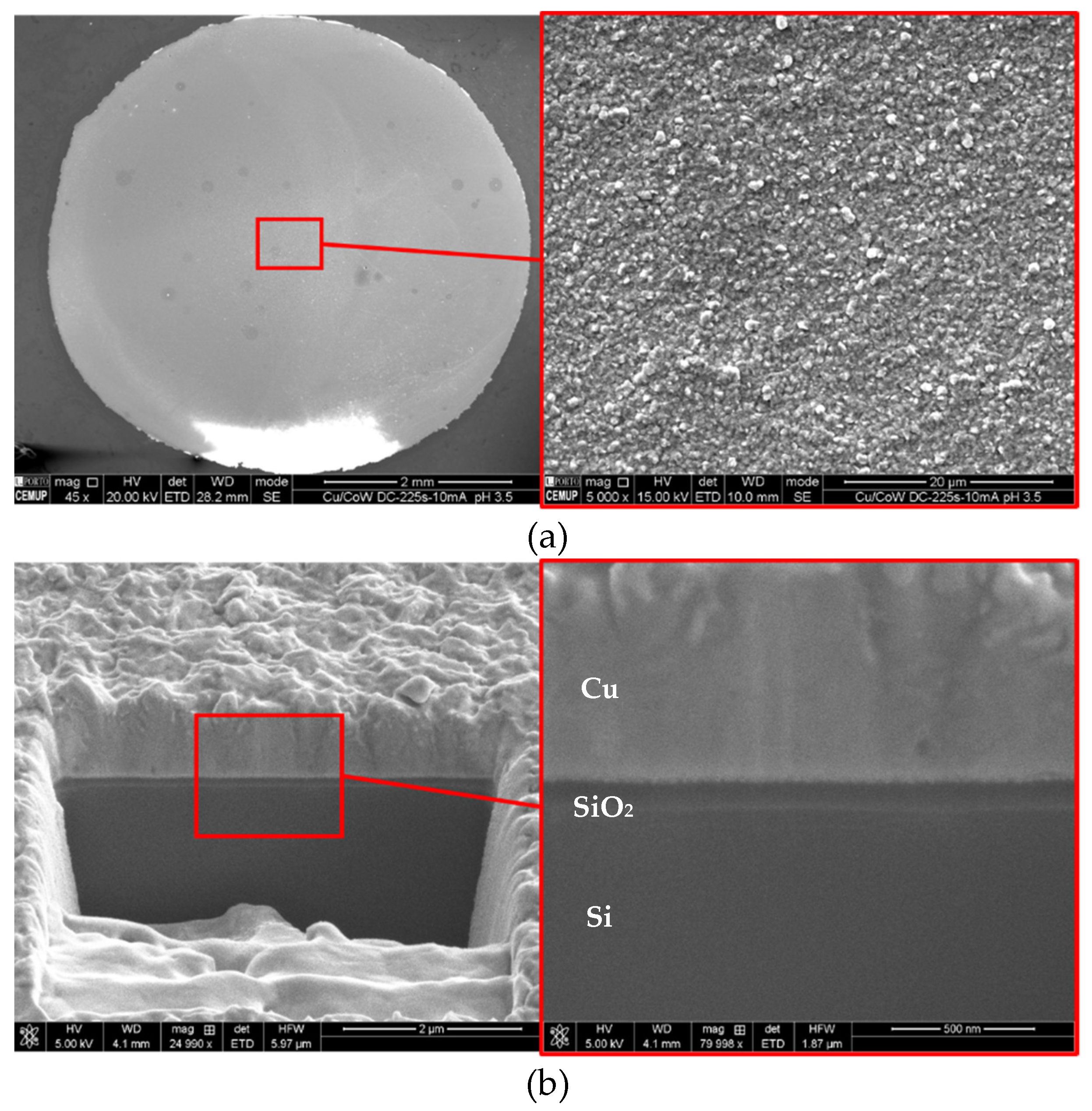
−2 with very different results. The outcome is a compact surface structure, covering the whole substrate area, as depicted in
Figure 12a. Cross-section imaging reveals a dense Cu film with thickness around 0.8–0.9 µm, with an average deposition rate of 3.5–4 nm/s and structural continuity across the Cu/Co-W/SiO
2/Si interfaces (
Figure 12b). Using Equation (5), a theoretical value of thickness,
, can be calculated, where
and
are the molecular mass and the density of Cu, respectively;
is the charge of the electron;
is the oxidation state for Cu ions; and
Avogadro’s number. The value of
obtained with 225 s of deposition at 10 mA·cm
−2 is 0.84 µm, corresponding very closely to the measured Cu cross-sectional thickness, indicating a deposition efficiency near 100%.
Although the Co-W film thickness is not possible to resolve in SEM, the region between SiO
2 and Cu displays a continuous morphology, suggesting a good Cu film adhesion to Co-W. Evidently, higher resolution imaging is required to fully characterise the Cu/Co-W interface, supplemented by adhesion tests to evaluate its strength. Nevertheless, it is very clear that an increase in electrolyte pH from 1.8 to 3.5 yields a remarkable improvement in substrate coverage and film morphology. Substrate dissolution is likely to be much slower in pH 3.5, resulting in a slower decrease in the number of active sites for nucleation due to W enrichment, allowing a higher nuclei density to be formed and a more homogeneous particle growth. A prior study [
24] demonstrated that a continuous Cu film can be effectively deposited onto Co using a neutral pH electrolyte containing copper sulphate and potassium sodium tartrate, where the dissolution of Co substrate is mitigated. However, the authors used a carbon-based activation pre-treatment on the Co surface to enhance deposition. In the present study, an increase in pH from 1.8 to 3.5 seems to be sufficient to prevent significant substrate dissolution, allowing a complete coverage and a sound interface. It is a much simpler and less disruptive approach from the current Cu interconnect technology standpoint.


 ,
, 


