Article

Silicon-Controlled Rectifier Embedded Diode for 7 nm FinFET Process Electrostatic Discharge Protection

1
Hangzhou Global Scientific and Technological Innovation Center, Zhejiang University, Hangzhou 310027, China
2
Engineering Product Development, Singapore University of Technology and Design, Singapore 138682, Singapore
*
Author to whom correspondence should be addressed.
Nanomaterials 2022, 12(10), 1743; https://0-doi-org.brum.beds.ac.uk/10.3390/nano12101743
Submission received: 16 April 2022 / Revised: 6 May 2022 / Accepted: 18 May 2022 / Published: 19 May 2022
(This article belongs to the Special Issue Abridging the CMOS Technology)

Abstract

:
A new silicon-controlled rectifier embedded diode (SCR-D) for 7 nm bulk FinFET process electrostatic discharge (ESD) protection applications is proposed. The transmission line pulse (TLP) results show that the proposed device has a low turn-on voltage of 1.77 V. Compared with conventional SCR and diode string, the proposed SCR-D has an additional conduction path constituting by two additional inherent diodes, which results in a 1.8-to-2.2-times current surge capability as compared with the simple diode string and conventional SCR with the same size. The results show that the proposed device meets the 7 nm FinFET process ESD design window and has already been applied in actual circuits.

1. Introduction

Electrostatic discharge (ESD)-induced damage is one of the main failures of integrated circuits. In the 7 nm FinFET process used in the state-of-the-art integrated circuits, the gate oxide of FinFET is extremely fragile under an electrostatic discharge (ESD) impact due to its reduced thickness and low reliability of high-k dielectric [1,2,3], and the ESD protection will degrade gradually after encountering non-fatal ESD strikes [4,5]. Some techniques for ESD modeling and simulation have been utilized in the FinFET process to help analyze the characteristics of ESD protection under ESD strike [6,7,8,9]. The ESD protection diodes are considered to be promising in advanced technology as an ESD protection device [6,7,8]. The diode-string silicon-controlled rectifier (DSSCR) with high robustness is also considered as the ESD protection device for previous technology nodes [10,11,12,13,14,15], but it is no longer suitable for the 7 nm technology due to its high leakage and large snapback for latch-up. ESD design for the FinFET process is still a great challenge. A high-robustness ESD-protection device with a sufficiently low trigger voltage (Vt) and high failure current (It2) is not yet available. In this letter, we propose a new silicon-controlled rectifier-embedded diode (SCR-D) based on the 7 nm FinFET process. The characteristics of this protection with different key designs are fabricated and analyzed.

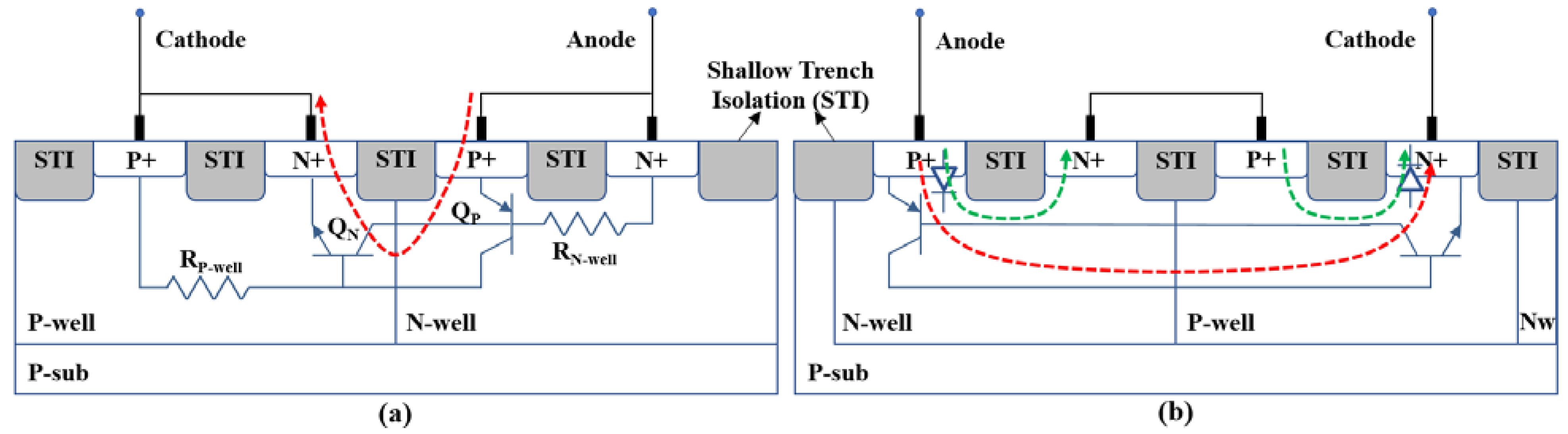
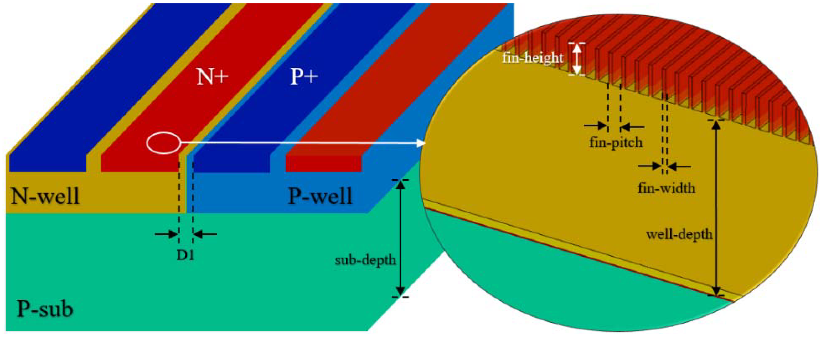
2. Design and Analysis

Figure 1a shows the cross-sectional view of a conventional SCR composing two bipolar transistors with two parasitic well resistors. When the SCR is turned on, the positive feedback path formed by the two transistors enables a large current flow between the cathode and anode to bypass the ESD current with a very small size; however, the turn-on time of the SCR is very long in the order of 20 ns, and the trigger voltage is too high to fit in the design windows of MOS technologies. In the modified structure SCR-D shown in Figure 1b, we introduce diodes to both the cathode and anode to reduce the trigger voltage. In contrast to Figure 1a, the P-well and N-well of the SCR-D are swapped, as is the cathode and anode, although the P+ and N+ junctions connected to the terminals and the fabrication process remain unchanged. This new arrangement results in two additional PN junctions and two different bipolar transistors. On the anode side, the PNP transistor is constituted by P+, N-well, and P-well, whereas the NPN transistor on the cathode side is constituted by N+, P-well, and N-well. This structure effectively increases the distance between cathode and anode, thus resulting in a larger holding voltage and a smaller snapback voltage.
Two-dimensional technology computer-aided design (TCAD) simulation was carried out to illustrate the operation of the devices. Figure 2 shows the current distribution of the SCR-D for two different situations. Figure 2a shows the low-level current conduction case. The major current-conduction path is via the anode diode (P+/N-well junction), to the metal wire connecting N-well and P-well and then the cathode diode (P-well/N+ junction). The two-diode string can release the initial ESD current. As the diode current in the anode increases to a certain level and triggers the avalanche breakdown of the reversely biased PN junction between the N-well and P-well (see Figure 2b), the SCR will be turned on. A significant amount of current flows from the anode to cathode via the N-well and P-well, and the current level of the conduction becomes high.

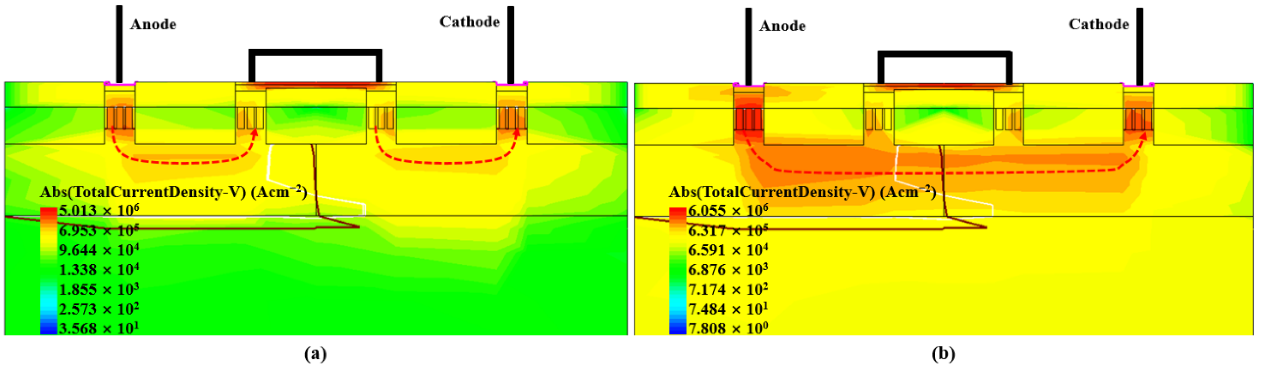
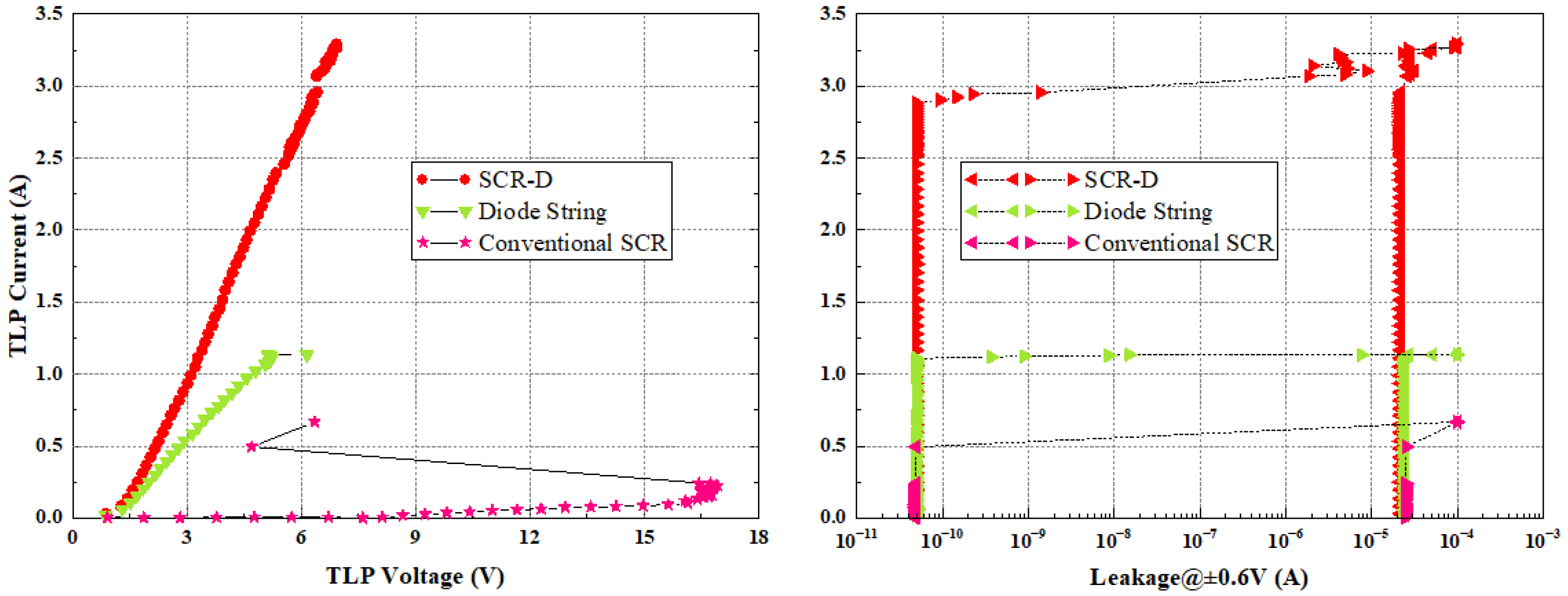
3. Result and Discussion
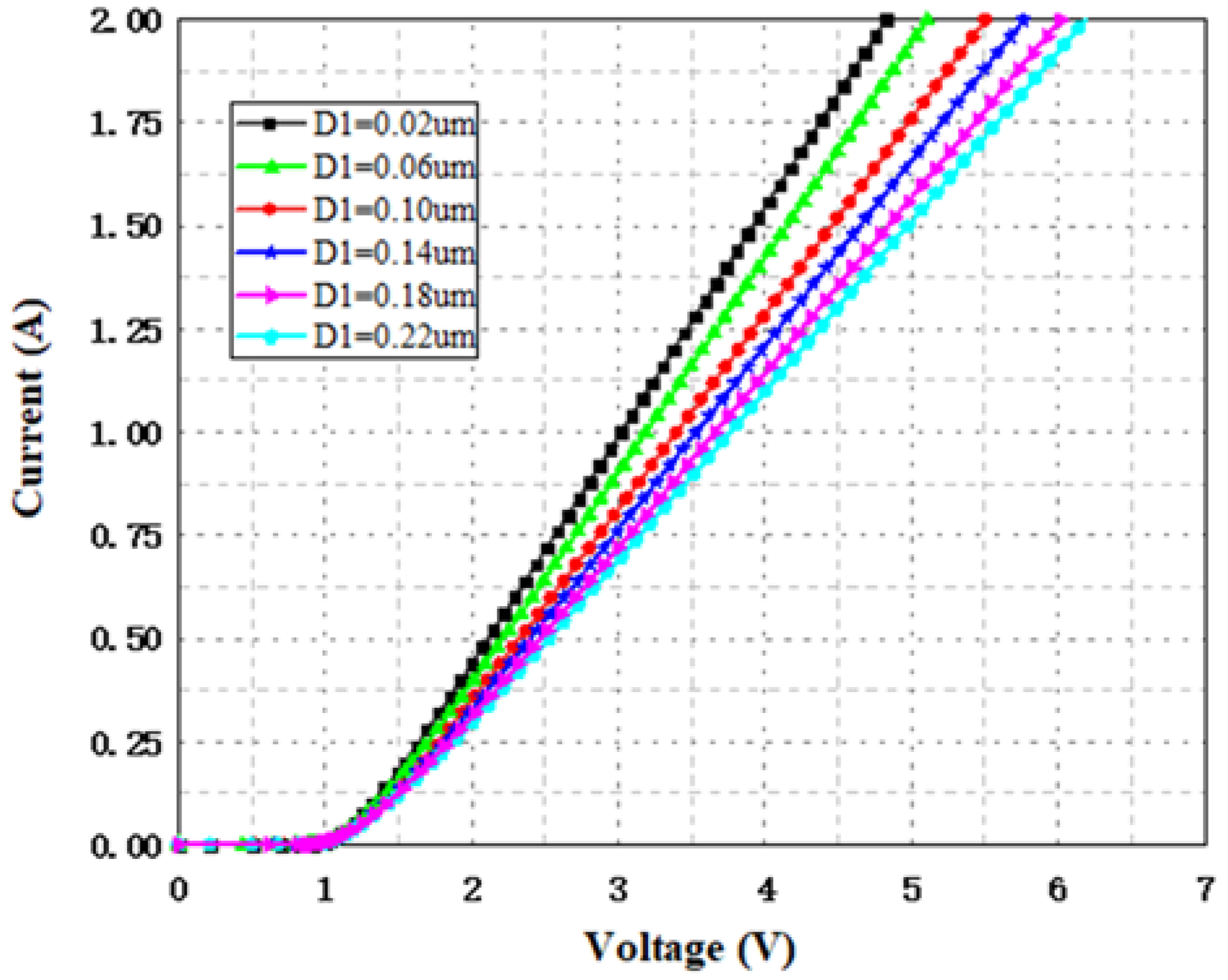
3.1. TLP Results

The TLP I-V characteristics of the diode string, conventional SCR and SCR-D are shown in Figure 3. It is noted that the conventional SCR is broken down almost immediately when it is turned on at 16 V. For the forward-biased two-diode string, although the turn-on voltage is 1.4 V, which can meet the 7 nm FinFET application requirement (1.1 V to 5 V), the failure current is very low (~1.2 A), which is not particularly suitable for the application. Increasing the failure current requires larger sizes of the diodes, which will result in a larger leakage current. For the new SCR-D structure, the trigger voltage is lowered to 1.77 V. The failure current (It2) of SCR-D increases to about 2.25 A, and the leakage current is below nA level because of the much smaller size of the diodes. Table 1 compares the characteristics of these three ESD protection devices. To have a fair comparison, we define the failure current per device area as the robustness figure-of-merit (FOM), as shown in the last column Table 1. For the same device area, SCR-D provides 80% more current-sinking capability than the two-diode string. The sinking current of SCR-D is about 2.2 times of that of the conventional SCR with the same device area.

3.2. Optimization Device Sturcture

Having verified the operation mechanism of the SCR-D in FinFET process with TCAD simulation, we will next simulate the effects of device parameters on the ESD protection characteristics of the SCR-D device. Different from the planar process, we need to consider the three-dimensional fin structure in FinFET process in the simulation. Figure 4 shows some parameters for SCR-D and parameters of the fin structure for TCAD simulation. We focus on the impact of the variation of key parameters on the device performance, such as the spacing between the N+ and P+ regions, which is represented as D1 in Figure 4. Table 2 shows the intrinsic parameters in FinFET process, which are fixed irrelevant to integrated circuit layout and are used in the TCAD simulation.
The lower trigger voltage and on-state resistance indicate that SCR-D has the combined advantages of the conventional SCR and diode string. When an ESD pulse comes, the trigger diode string conducts first, which takes part of the trigger voltage, and then the SCR path is turned on, providing a low-resistance current discharge through not only through the surface of silicon but also the bulk. Figure 5 simulates the I-V curve of SCR-D with different D1 values. The simulation results are summarized in Table 3, which show that a smaller D1 value is required to reduce the trigger voltage and on-state resistance.

4. Conclusions

A new silicon-controlled rectifier embedded diode (SCR-D) is proposed for 7 nm FinFET process by swapping the N-well and P-well in the conventional SCR process. The new SCR-D introduces two additional diodes that provide an additional low-current conduction path to reduce the trigger voltage to about 1.77 V and enhance the maximum conducting current by about 1.8-to-2.2 times, respectively, as compared with the diode string and conventional SCR with the same device size. These parameters meet the design window specifications as derived from the 7 nm FinFET process. The proposed SCR-D does not need any additional process steps and can be applied in an actual circuit.

Author Contributions

Methodology, X.Z., S.D. and F.Y.; investigation, F.D., K.S., K.L.P. and J.L.; data curation, X.Z., F.Y., F.D. and K.S.; writing—original draft preparation, X.Z., F.Y., K.S., K.L.P. and J.L.; writing—review and editing, S.D., K.S. and J.L.; project administration, X.Z.; funding acquisition, K.S. and J.L. All authors have read and agreed to the published version of the manuscript.

Funding

This research and the APC was funded in part by the NSFC-Zhejiang Joint Fund for the Integration of Industrialization and information under the grant of U20A20172, and in part by the Zhejiang Province Key Research & Development Project under the grant of 2021C05004.

Institutional Review Board Statement

Not applicable.

Informed Consent Statement

Not applicable.

Data Availability Statement

Not applicable.

Acknowledgments

We thank ESDEMC Technology LLC for TLP testing.

Conflicts of Interest

The authors declare no conflict of interest.

References

  1. Wong, H.; Iwai, H. On the scaling of subnanometer EOT gate dielectrics for ultimate nano CMOS technology. Microelectron. Eng. 2015, 138, 57–76. [Google Scholar] [CrossRef]
  2. Wong, H.; Zhou, J.; Zhang, J.; Jin, H.; Kakushima, K.; Iwai, H. The interfaces of lanthanum oxide-based subnanometer EOT gate dielectrics. Nanoscale Res. Lett. 2014, 9, 472. [Google Scholar] [CrossRef] [PubMed] [Green Version]
  3. Wong, H. Nano-CMOS Gate Dielectric Engineering; CRC Press: Boca Raton, FL, USA, 2012; pp. 1–234. [Google Scholar]
  4. Wong, H.; Dong, S.; Chen, Z. On the ESD Protection and Non-Fatal ESD Strike on Nano CMOS Devices. In Proceedings of the IEEE 31st International Conference on Microelectronics (MIEL), Nis, Serbia, 16–18 September 2019; pp. 3–8. [Google Scholar]
  5. Wu, J.; Rosenbaum, E. Gate oxide reliability under ESD-like pulse stress. IEEE Trans. Electron Devices 2004, 51, 1528–1532. [Google Scholar] [CrossRef]
  6. Li, Y.; Miao, M.; Gauthier, R. ESD Protection Design Overview in Advanced SOI and Bulk FinFET Technologies. In Proceedings of the IEEE Custom Integrated Circuits Conference (CICC), Boston, MA, USA, 22–25 March 2020; pp. 1–4. [Google Scholar]
  7. Linten, D.; Hellings, G.; Chen, S.-H.; Groeseneken, G. ESD in FinFET technologies: Past learning and emerging challenges. In Proceedings of the IEEE International Reliability Physics Symposium (IRPS), Monterey, CA, USA, 14–18 April 2013; pp. 2B.5.1–2B.5.8. [Google Scholar]
  8. Chen, S.-H. ESD Challenges in Advanced FinFET and GAA Nanowire CMOS Technologies: Designing Diode Based ESD Protection in Advanced State of the Art Technologies. In Proceedings of the IEEE Custom Integrated Circuits Conference (CICC), Austin, TX, USA, 14–17 April 2019; pp. 1–100. [Google Scholar]
  9. Li, Y.; Wang, Y.; Wang, Y. ESD Diode Devices Simulation and Analysis in a FinFET Technology. In Proceedings of the International EOS/ESD Symposium on Design and System (IEDS), Chengdu, China, 23–25 June 2021; pp. 1–4. [Google Scholar]
  10. Song, S.; Du, F.; Hou, F.; Song, W.; Liu, Z.; Liu, J. A New dual directional SCR with high holding voltage for High Voltage ESD protection. In Proceedings of the IEEE International Conference on Electron Devices and Solid-State Circuits (EDSSC), Xi’an, China, 12–14 June 2019; pp. 1–2. [Google Scholar]
  11. Huang, X.; Liu, Z.; Liu, F.; Liu, J.; Song, W. High holding voltage SCRs with segmented layout for high-robust ESD protection. Electron. Lett. 2017, 53, 1274–1275. [Google Scholar] [CrossRef]
  12. Lin, L.; Gauthier, R.; Loiseau, A.; Lu, X. Design optimization of a breakdown silicon controlled rectifier (BDSCR) for cell phone antenna switch pin electrostatic discharge (ESD) protection. In Proceedings of the Electrical Overstress/Electrostatic Discharge Symposium Proceedings, Reno, NV, USA, 23–28 September 2018; pp. 1–8. [Google Scholar]
  13. Liang, H.; Xu, Q.; Zhu, L.; Gu, X.; Sun, G.; Lin, F.; Zhang, S.; Xiao, K.; Yu, Z. Design of a Gate Diode Triggered SCR for Dual-Direction High-Voltage ESD Protection. IEEE Electron Device Lett. 2019, 40, 163–166. [Google Scholar] [CrossRef]
  14. Lai, D.-W.; Tseng, W.-J.; De Raad, G.; Smedes, T. DNW-controllable triggered voltage of the integrated diode triggered SCR (IDT-SCR) ESD protection device. In Proceedings of the 39th Electrical Overstress/Electrostatic Discharge Symposium (EOS/ESD), Tucson, AZ, USA, 10–14 September 2017; pp. 1–9. [Google Scholar]
  15. Du, F.; Song, W.; Hou, F.; Liu, J.; Liu, Z.; Liou, J.J.; Xiong, X.; Li, Q.; Liu, Y. Augmented DTSCR With Fast Turn-On Speed for Nanoscale ESD Protection Applications. IEEE Trans. Electron Devices 2020, 67, 1353–1356. [Google Scholar] [CrossRef]
Figure 1. Cross-sectional views of SCR structures: (a) conventional SCR device;(b) SCR-D proposed in this work. Color lines indicate the current flow when it is turned on.
Nanomaterials 12 01743 g001
Figure 2. TCAD simulated current distribution of SCR-D at different stages: (a) low ESD current; (b) large ESD current.
Nanomaterials 12 01743 g002
Figure 3. TLP I-V characteristics and leakage measured from diode string, conventional SCR, and SCR-D proposed in this work.
Nanomaterials 12 01743 g003
Figure 4. SCR-D parameters in TCAD simulation; enlarged view of Fin structure.
Nanomaterials 12 01743 g004
Figure 5. I-V curves for SCR-D in TCAD simulation with different D1 values.
Nanomaterials 12 01743 g005
Table 1. Comparison of the key parameters of three ESD protection devices.
DeviceTrigger Voltage (V)It2 (A)Robustness (mA/μm2)
SCR16.90.102.70
2-diode string1.401.203.30
SCR-D1.772.255.96
Table 2. The intrinsic parameters in FinFET process used in simulation.
Size NameValue (μm)Doping RegionValue (cm3)
sub-depth10.000P-sub1 × 1015
well-depth0.450P-well1.9 × 1018
fin-height0.070N-well1.9 × 1018
fin-width0.008P+1.2 × 10²¹
fin-pitch0.030N+1.2 × 10²¹
Table 3. Comparison of the key parameters of SCR-D with different D1 values.
D1 (μm)0.020.060.100.140.180.22
Trigger Voltage (V)1.3241.3511.3851.4041.4191.436
On-State Resistance (Ω)1.811.922.112.242.372.45
Publisher’s Note: MDPI stays neutral with regard to jurisdictional claims in published maps and institutional affiliations.

