Article

Plasma-Wind-Assisted In2S3 Preparation with an Amorphous Surface Structure for Enhanced Photocatalytic Hydrogen Production

1
College of Chemistry, Taiyuan University of Technology, Taiyuan 030024, China
2
Department of Chemical Engineering, Imperial College London, South Kensington Campus, London SW7 2AZ, UK
3
Department of Mechanical Engineering, University of Delaware, Newark, DE 19716, USA
4
Key Laboratory of Interface Science and Engineering in Advanced Material, Ministry of Education, Taiyuan University of Technology, Taiyuan 030024, China
*
Authors to whom correspondence should be addressed.
Nanomaterials 2022, 12(10), 1761; https://0-doi-org.brum.beds.ac.uk/10.3390/nano12101761
Submission received: 27 April 2022 / Revised: 17 May 2022 / Accepted: 20 May 2022 / Published: 21 May 2022
(This article belongs to the Topic Catalysis for Sustainable Chemistry and Energy)

Abstract

:
Photocatalytic production from water is considered an effective solution to fossil fuel-related environmental concerns, and photocatalyst surface science holds a significant interest in balancing photocatalysts’ stability and activity. We propose a plasma-wind method to tune the surface properties of a photocatalyst with an amorphous structure. Theoretical calculation shows that the amorphous surface structure can cause an unsaturated coordination environment to adjust the electron distribution, forming more adsorption sites. Thus, the photocatalyst with a crystal–amorphous (C–A) interface can strengthen light absorption, harvest photo-induced electrons, and enrich the active sites, which help improve hydrogen yield. As a proof of concept, with indium sulfide (In2S3) nanosheets used as the catalyst, an impressive hydrogen production rate up to 457.35 μmol cm−2 h−1 has been achieved. Moreover, after plasma-assisted treatment, In2S3 with a C–A interface can produce hydrogen from water under natural outdoor conditions. Following a six-hour test, the rate of photocatalytic hydrogen evolution is found to be 400.50 μmol cm−2 g−1, which demonstrates that a catalyst prepared through plasma treatment is both effective and highly practical.

Graphical Abstract

1. Introduction

Overusing fossil fuels is the primary cause of global environmental problems and the energy crisis. Photocatalytic hydrogen production from water is a promising green route to address such issues. With its high energy density, hydrogen gas is a clean replacement for fossil fuels [1,2,3,4,5]. However, a significant obstacle to the industrialization of photocatalytic hydrogen production is low conversion efficiency. Many strategies have been therefore proposed to enhance the optical, electrical, and catalytic properties of photocatalysts to improve their efficiency, including heterojunction structural design [6,7], the introduction of plasmonic materials [8,9,10], defect engineering (e.g., oxygen or sulfur vacancy) [11,12], phase transition [13,14], and single-atom catalysis [15,16,17]. It is worth noting that catalysis is a surface redox reaction on the photocatalyst, where the water molecules split into hydrogen and oxygen [18]. Therefore, it makes sense to tune and improve the surface structure of photocatalysts to enhance their reactive interface with water molecules. However, some photocatalysts’ surface structure can usually be adversely affected in the liquid water environment, degrading catalytic stability and the chemical reaction. Thus, any industrially promising photocatalyst for hydrogen evolution reaction should balance material stability and activity with a harmonized surface structure design.
We report a plasma-wind strategy to realize the “surface amorphous engineering” to improve photocatalysts’ surface structure. A photocatalyst with a crystalline–amorphous (C–A) interface can boost light absorption and accelerate charge transfer [19,20,21]. In this work, In2S3 nanosheets are used as a typical catalyst with plasma treatment to obtain a tunable amorphous surface structure. In2S3 is a standard IIIA-VIA semiconductor that can be prepared through sol–gel or hydrothermal methods. This nanosheet has been researched as a visible-light-driven photocatalyst for water splitting and degradation [22,23,24,25]. Based on experimental observations and theoretical calculations, the coordination environment in the In2S3 nanosheet has been tuned through the plasma treatment. Thus, plasma-treated In2S3 (P-In2S3) with rich active sites has been achieved. Furthermore, considering the convenience of this plasma treatment, we have tested a practical model under natural outdoor conditions for further development, which displays the potential of this technique for industrialization.

2. Materials and Methods

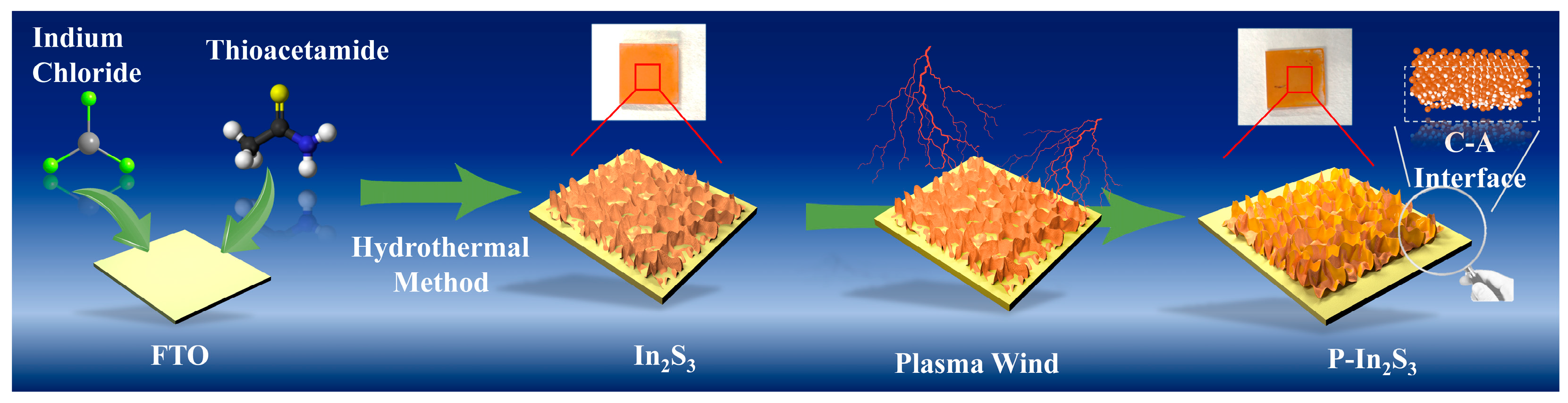
2.1. Synthesis of the In2S3

FTO glass was pre-cleaned through ultrasonic cleaning in ultrapure water and ethanol. After that, FTO glass was further treated with UV cleaning. InCl3 (0.05 g), thioacetamide (0.05 g), and the treated FTO glass were added into a Teflon-lined stainless steel autoclave. Then, 40 mL of ultrapure water was added to obtain a mixed solution. The autoclave was heated at 150 °C (about 0.4 MPa) for 6 h and cooled to room temperature naturally. Hereafter, the resulting samples were named In2S3.

2.2. Synthesis of the P-In2S3

The prepared In2S3 in FTO was placed in the plasma-treatment device (AC220-2g). The Ar gas was the carrier gas, and the time was set for 60 min. The power was 200 W. The chamber pressure was 200 Torr, and the Ar flow rate was 50 cc min−1. The sample was placed 25 mm away from the powered electrode. Then, after the reaction, the P-In2S3 was obtained.

2.3. Characterization of the Photocatalysts

The morphology and structure of the samples were characterized using a scanning electron microscope (SEM) (FEI NOVA 450, FEI Company, Hillsboro, OR, USA) and transmission electron microscope (TEM) (FEI Talos F200X). The absorption spectrum was measured using an ultraviolet-visible (UV-Vis) spectrophotometer (Perkin-Elmer Lambda 35 UV-VIS-NIR, Waltham, MA, USA). The electrochemical workstation (Chenhua 760e, CH Instruments, Shanghai, China) was used for the photoelectric performance test. The EIS at a frequency range from 100 kHz to 1 Hz was measured. The Raman spectra were collected through the Renishaw with the 532 nm laser. During the catalytic measurements, the Raman spectra were collected at the same interval voltage to eliminate the extra influence induced through bias voltage (the measurement voltage was 0.05, 0.00, −0.05, −0.10, and −0.15 V) under the same light intensity (5 mW), and the exposure time was 5 s.

2.4. Photocatalytic Activity

The photocatalytic reaction was conducted by photocatalysts (1 cm−2) with 50 mL of deionized water in a quartz cell, loaded with 0.3 M Na2S and 0.3 M Na2SO3 as hole scavengers. A light source was equipped with a fin-like heat sink for dissipating excessive heat effectively. The incident power was measured by a power meter. The average power was determined to be 100 mW cm−2. The gases evolved during the photocatalytic reaction and were transferred into a sample loop by a peristaltic pump. They were further quantified using gas chromatography (Shimadzu GC-2014c (Kyoto, Japan), Ar carrier gas, and molecular sieve-5A column), equipped with a thermal conductivity detector (TCD) with a set temperature of 422 K. The yield of hydrogen gas produced from the reactor was measured every 15 min. For the cyclic test, the reactor is replenished with 0.3 M Na2S and 0.3 M Na2SO3 and degassed in a vacuum before starting the irradiation for another measurement.

2.5. Computational Details

All calculations presented here were implemented in the Vienna ab initio simulation package (VASP 5.4, Hafner Group, Wien, Austria) [26]. The generalized gradient approximation (GGA) in Perdew–Burke–Ernzerhof (PBE) format was used for the exchange-correlation function [27]. The long-range van der Waals interaction was described by the DFT-D3 approach [28]. The cut-off energy for the plane wave was set at 400 eV. The energy and force convergence criteria for structure relaxations were 0.1 meV/atom and 0.03 eV/Å, respectively. The geometry was optimized with a 3 × 3 × 1 k-mesh grid.
The bulk In2S3 constituted 80 atoms, the lattice parameters were obtained by fully relaxing the structure, and the obtained a and c were 7.74 Å and 32.85 Å, respectively. Amorphous In2S3 structure was constructed by density functional theory molecular dynamics (DFT-MD). The atoms in the crystal structure were melted at 2000 K for 7000 MD steps and quenched from 2000 to 300 K for 7000 MD steps [29]. A surface model of In2S3 in (002) orientation was created based on the optimized crystal and amorphous bulk geometry. A vacuum region of 15 Å was added perpendicular to the sheet to avoid artificial interaction between periodic images; the bottom layers of the slabs were fixed during relaxation.
The free energies were calculated by treating the H adsorbate within the harmonic oscillator approximation, which is given by Δ G = Δ E   + Δ ZPE   T Δ S , where Δ ZPE and Δ S are the changes in the zero-point energy and entropy, respectively, and T is the temperature of 298.15 K.

3. Results and Discussion

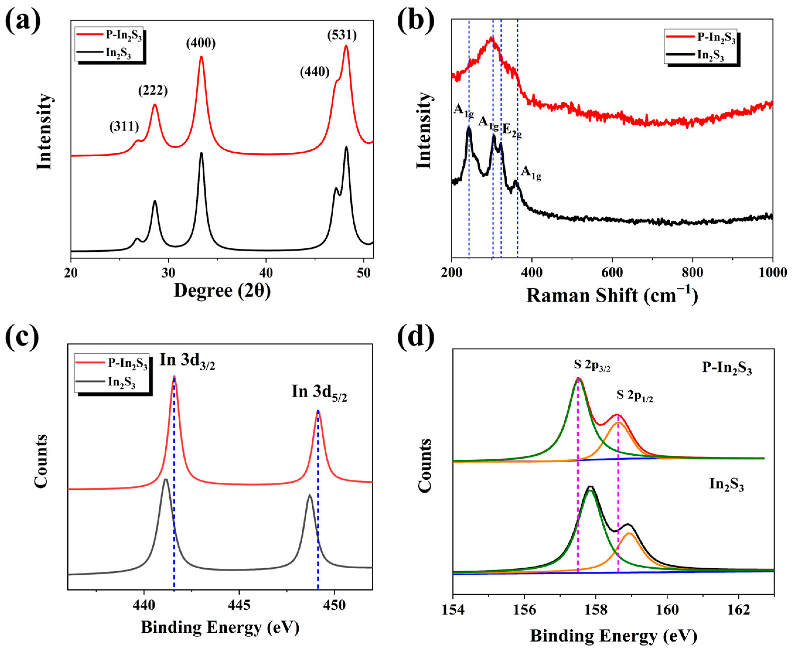
3.1. The Synthesis Process and Related Morphological, Spectroscopic Characterization

As shown in Figure 1, indium chloride and thioacetamide are used to prepare the In2S3 nanosheets. The nucleation event of In2S3 nanosheets takes place on the surface of fluorine-doped tin oxide (FTO) glass. The In2S3 nanosheets are distributed uniformly on the surface of the FTO glass, and the assembly is then subject to plasma treatment. Thus, the plasma-wind-assisted In2S3 (P-In2S3) with a C–A interface is obtained. Compared to bare In2S3 nanosheets, there is a slight difference in the surface gloss of the P-In2S3 nanosheets.
Both samples are measured for further analyzing the surface structure. As shown in Figure S1, the morphology and the crystalline structure of the In2S3 sample are displayed, and the nanosheets grow vertically on the substrate. Figure 2 illustrates the morphology and structure of the P-In2S3 sample. Similarly, the SEM image in Figure 2a shows that the P-In2S3 sheets are vertically distributed on the substrate. As shown in Figure 2b, the nanosheets are tangled with the black lines on the nanosheet edges, most notably the gradually structural changing of the crystalline–amorphous (C–A) interface in Figure 2c. The four box areas in Figure 2c show Fourier transforms. Witness how the demonstrating microstructure changes from box 1 to box 4. Furthermore, the HRTEM and the related filtered images (Figure 2d,e) show that the lattice fringes are inconsecutive, and some of the lattice fringes are ambiguous, indicating the existence of an amorphous region.
To obtain the structural information, X-ray diffraction (XRD), Raman, and X-ray spectroscopy (XPS) are used to analyze the samples. In Figure 3a, the XRD patterns of both In2S3 and P-In2S3 nanosheets are indexable with the standard powder diffraction card #84-1385. The peaks of the bare In2S3 nanosheets located at 2θ degrees of 27.2°, 28.5°, 33.5°, 47.1°, and 48.2° are attributed to crystal faces (311), (222), (400), (440), and (531), respectively. After the plasma treatment, there is little change in the crystal face position but the weakened intensity of the crystal face (440), exhibiting robust long-range lattice arrangement and short-range structure conversion. As shown in Figure 3b, the different vibration modes, A1g and E2g of In2S3, are d, with the related Raman peaks located at 244.23, 305.96, 320.69, and 360.40 cm−1, respectively [30,31]. After plasma treatment, the Raman vibration modes have been heavily altered. The Raman vibration modes are affected by local atomic arrangement, including factors such as stress, defects, and structural disorder [31], thus exhibiting the partial conversion of the atomic structure.
The XPS spectra further explore the conversion of crystal structure due to plasma treatment. Figure 3c shows high-resolution XPS spectra of elemental indium from samples. The In 3d3/2 and 3d5/2 peaks at 441.1 and 448.7 eV for the bare In2S3 nanosheets red-shift to 441.6 and 449.2 eV for the P-In2S3 nanosheets, respectively [32]. The red-shift of In binding energy shows that the electron cloud density of In atoms is reduced to indicate the coordination structure variation. Additionally, the sulfur’s 2p3/2 and 2p1/2 peak locations at 157.8 and 158.9 eV show a b (Figure 3d), indicating the electron cloud density around the S atom has increased [33,34], which would favor the hydrogen adsorption. All these measurements show that the atomic structure of In2S3 nanosheets can be altered through the plasma treatment, confirming the C–A interface present in the P-In2S3 nanosheets.

3.2. The Photocatalytic Hydrogen Production Performance

The photocatalytic reaction activity is mainly controlled by optical properties, electronic structure, and catalytic reactivity. First, as shown in Figure 4a, the light absorption spectra of the two samples have been measured, and the P-In2S3 sample has better light absorption compared with bare In2S3. This implies that plasma treatment is an effective way of improving photocatalyst optical absorption. The highest apparent quantum yield (AQY) of bare In2S3 is just 20.1% at 380 nm, whereas the AQY of P-In2S3 at 380 nm and 420 nm is 26.2% and 19.8%, respectively.
As for electronic properties, as shown in Figure 4b, the bandgap (Eg) of these two materials can be calculated based on the UV-vis light absorption spectra. The bandgap of bare In2S3 is about 1.7 eV; it is about 1.5 eV for P-In2S3, which is beneficial to the use of visible light in the catalytic reaction. The Mott–Schottky (MS) curves of the samples are used to evaluate the carrier density (Figure 4c) preliminarily. The MS curve slope of P-In2S3 is larger than that of bare In2S3, indicating that more charge carriers exist in the P-In2S3 sample under illumination. As a result of the positive values of these MS slopes, the two samples behave as n-type semiconductors [35]. Considering that the conduction band is near the flat potential in an n-type semiconductor, the conduction bands of P-In2S3 and bare In2S3 are estimated to be −0.47 eV and −0.45 eV, respectively. Based on this analysis, the energy band structure can be summarized in Figure 4d, where the conduction band of P-In2S3 is more negative to the H+/H2 potential than that of In2S3, favoring the hydrogen production reaction in water molecules splitting. The changing trend of electron structure is also supported by the theoretical calculations (Figures S2 and S3).
The optical–electrical property is also mined through the photocurrent density, as shown in Figure 4e. The photocurrent density of P-In2S3 is about 0.48 mA cm−2, which is 2.4 times higher than that of In2S3 (0.21 mA cm−2). Such high photocurrent density results in a highly effective hydrogen production reaction. The charge separation efficiency (ηsep) of the sample is calculated based on the equation
η s e p = J s u l f i t e J a b s
where Jsulfite is the photocurrent density with the addition of Na2SO3 in the electrolyte solution, Jabs is the photocurrent density when the adsorbed photons completely convert to currents. The calculated process is presented in supporting information [36,37]. The photocurrent densities Jsulfite of the In2S3 and P-In2S3 samples are measured to be 0.21 and 0.48 mA cm−2, as shown in Figure 5e, and the Jabs of the In2S3 and P-In2S3 samples are calculated to be 0.51 and 0.85 mA cm−2, respectively. Thus, the ηsep values of the In2S3 and P-In2S3 are 41.3 % and 56.2 %, respectively, exhibiting that the plasma treatment can regulate the electronic structure to accelerate the separation of the charge carriers. In addition, the electrochemical impedance curves of the P-In2S3 and bare In2S3 samples are measured and shown in Figure 4f, where a smaller arc radius is observed for the P-In2S3 sample, implying faster interfacial electron transfer. The equivalent circuit of the impedance curve fitting of the resistance–capacitance scheme is displayed, and the addition of the C–A interface resulting from plasma treatment plays a crucial role in boosting electron transfer.
The active electrochemical area is a significant indication of the catalytic reaction property of the sample. As shown in Figure S4, the electrochemical surface area in bare In2S3 is about 3.62 mF cm−2, whereas, with P-In2S3, the electrochemical surface area is 10.88 mF cm−2, which favors hydrogen adsorption in a catalytic reaction.
Moreover, the hydrogen adsorption process is further explored through the operando Raman measurement displayed in Figure 5a and Figure S5. Both bare In2S3 and P-In2S3 samples are deposited on the FTO as the working electrode. The counter and reference electrodes are platinum and silver/silver chloride (saturated potassium chloride electrolyte). After hydrogen adsorption to the active regions of the catalyst surface, intermediate bonds can form and be detected by Raman. At the same time, linear sweep voltammetry curves are measured to monitor the catalytic reaction stage, as shown in Figure 5b. As potential increases in value, the current density also increases in value. At the same potential, the current density of P-In2S3 is higher than that of bare In2S3, indicating more reactive electrons in the P-In2S3 sample. At different potentials, specifically −0.05, −0.10, −0.15, and −0.20 V, Raman spectra are collected to analyze hydrogen adsorption in the catalytic reaction (Figure 5c and Figure S6). The Raman peak at 2611 cm−1 is attributed to the S−H Raman vibration [38], which implies that the active sites are the sulfur atoms to adsorb the hydrogen atoms. Figure 5c shows that S−H Raman intensity rises with increased potential, suggesting that more hydrogen adsorption can be realized at a relatively high potential range. Importantly, it is noticed that the S−H Raman intensity of P-In2S3 is higher than that of bare In2S3 at any given potential, indicating that more hydrogen atoms are adsorbed onto the P-In2S3 surface during the catalytic reaction process compared with that of bare In2S3 (Figure S7).
The theoretical calculation is applied to analyze the catalytic performance of hydrogen adsorption (Figure 5d and Figure S8). About 0.373 (e) electron transfer on the amorphous surface, which is larger than that on the crystal surface (0.282 (e)). The Gibbs free energy of the hydrogen adsorption is calculated in Figure 5e, and a value closer to zero corresponds to better hydrogen adsorption performance [39]. On the crystal–amorphous surface, the free energy of the hydrogen adsorption is −0.27 eV, which is closer to zero than that on the crystal surface (−0.37 eV) in value (i.e., the absolute value of free energy of the hydrogen adsorption on the crystal–amorphous surface is smaller than that on the crystal surface), indicating that the crystal–amorphous surface favors the hydrogen adsorption.
Photocatalytic hydrogen production is measured with different samples, as shown in Figure 6a. The sacrificial agents of 0.3 M Na2S and 0.3 M Na2SO3 are used to capture photo-induced holes. At the end of a 120 min test, the amount of hydrogen production with bare In2S3 is about 337.5 μmol, and the average hydrogen production rate is calculated to be 168.60 μmol cm−2 h−1. In comparison, hydrogen production with P-In2S3 is about 914.7 μmol after 120 min, and the average hydrogen production rate is estimated to be 457.35 μmol cm−2 h−1 (the mass catalyst: 133 mg, converted rate 3438.72 μmol h−1 g−1). The comparison of the measurement data from this work with other references, including the hydrogen production rate, current density, and bandgap, has been made in Table S1 in the supporting information, exhibiting that the photocatalytic performance of P-In2S3 is dominant in these In2S3-based catalysts. These results have shown that plasma treatment can substantially enhance photocatalytic hydrogen production from water. It is easily observed from Figure 6b that the level of hydrogen production after the seventh test (about 840 min) is slightly smaller than that of the initial stage for P-In2S3, which is in sharp contrast to the catalytic performance of bare In2S3, which shows drastic reduction of hydrogen production after only four test cycles, exhibiting high stability in the photocatalytic reaction of P-In2S3, also reflected by the morphology and structure of the samples (Figures S9 and S10).
A schematic of the photocatalytic hydrogen production reaction using P-In2S3 is shown in Figure 6c. After the plasma treatment of bare In2S3, the atomic arrangement of the nanosheets is altered to form an amorphous surface layer based on the bombardment from the plasma gas [40,41,42]. The amorphous region in the In2S3 nanosheets creates an unsaturated coordination environment to tune the electron structure. Therefore, P-In2S3 nanosheets with a C–A interface can improve light absorption and electron transfer. Moreover, the unsaturated coordination environment from the amorphous region endows the electrons gathering around S atoms, providing rich active sites for the catalytic reaction, thus leading to a highly efficient hydrogen production reaction.
A practical demo of the P-In2S3 photocatalytic system to satisfy real-world conditions is shown in Figure 6d. The P-In2S3 catalysts are laid on the surface of a perforated diaphragm, and the photocatalyst construction is immersed in water with the sacrificial agent. Owing to the transparency of the reactor, natural sunshine can illuminate the catalytic system. The reaction chamber outlet is connected to a gas collector, and the collected gas is detected through gas chromatography (GC) every two hours. A molecular hydrogen (H2) GC signal is detected, showing that the photocatalytic reaction works under natural outdoor conditions (Figure 6e). Three two-hour measurements are also shown in Figure 6f with a rate of H2 production of about 400.96 μmol cm−2 g−1 at the first 2 h, and the production rate of 400.50 μmol cm−2 g−1 after the 6 h test, indicating excellent stability.

4. Conclusions

We have designed and demonstrated a plasma-wind strategy for preparing In2S3 with an amorphous surface. We can achieve a photocatalytic water-splitting hydrogen production rate of 457.35 μmol cm−2 h−1 with high stability. Such impressive performance is due to the C–A interface, which improves light absorption and boosts charge carrier transfer to gather photo-induced electrons on the catalyst surface better. More importantly, the surface amorphous structure can cause an unsaturated coordination environment and gather electrons around the S atoms. In addition, the active reaction sites can be enriched as a result of the disordered atomic structure. This C–A interface can effectively balance catalytic activity and stability. Extending the P-In2S3 photocatalytic system under natural light conditions, a catalytic hydrogen production rate of 400.50 μmol cm−2 g−1 has been achieved, hopefully taking photocatalytic water splitting to a whole new level in practical energy applications.

Supplementary Materials

The following supporting information can be downloaded at: https://0-www-mdpi-com.brum.beds.ac.uk/article/10.3390/nano12101761/s1, Figure S1: (a) The SEM image, (b) the TEM image, and (c) the HRTEM image of the In2S3 sample. The inset is the Fourier transform of the black box area, and (d) the magnified HRTEM image of the In2S3 sample. The inset is the diffraction pattern of the sample; Figure S2: The material structures from the theoretical calculations. The yellow spheres are S atoms, and the purple spheres are In atoms; Figure S3: (a) The band structure of the crystal In2S3, (b) the band structure of the crystal–amorphous In2S3; Figure S4: (a) Electrochemical active area of the In2S3. The inset is the CVs of the In2S3 with different scan rates and (b) the Electrochemical active area of the P-In2S3. The inset is the CVs of the P-In2S3 with different scan rates; Figure S5: The photo of the operando Raman measurement; Figure S6: The potential impact on the operando Raman intensity of the bare In2S3 sample; Figure S7: The S–H bond Raman intensity after background subtraction versus the different potential during the operando Raman measurement; Figure S8: The hydrogen adsorption on the crystal surface and crystal–amorphous surface. The yellow spheres are S atoms, and the purple spheres are In atoms. The white sphere is the adsorption H atom; Figure S9: The morphology of the sample after the catalytic reaction. (a) bare In2S3, (b) P-In2S3. It is noticed that the surface of the bare In2S3 has been destroyed through the HRTEM imaging; comparatively, the structure of the P-In2S3 is well maintained; Figure S10: The Raman spectra of the P-In2S3 sample before and after catalytic reaction; Table S1: The comparison of hydrogen production rate, morphology, current density, and bandgap. References [24,25,43,44,45,46,47,48] are cited in the supplementary materials.

Author Contributions

Conceptualization, S.G.; validation, S.G. and H.L.; writing—original draft preparation, S.G.; writing—review and editing, H.L. and X.D.; supervision, B.W. and X.Z.; funding acquisition, S.G., X.D. and X.Z. All authors have read and agreed to the published version of the manuscript.

Funding

This study was financially supported by the Youth Science Research Project of Shanxi Province (No. 202103021223053), the Natural Science Foundation of Shanxi Province (No. 20210302123107), the National Natural Science Foundation of China (NSFC 21871167), and 1331 Project of Shanxi Province.

Data Availability Statement

Data presented in this article is available on request from the corresponding author.

Acknowledgments

Thanks to the assistance from Jia Xu.

Conflicts of Interest

The authors declare no conflict of interest.

References

  1. Chen, R.; Wang, Y.; Ma, Y.; Mal, A.; Gao, X.Y.; Gao, L.; Qiao, L.; Li, X.B.; Wu, L.Z.; Wang, C. Rational design of isostructural 2D porphyrin-based covalent organic frameworks for tunable photocatalytic hydrogen evolution. Nat. Commun. 2021, 12, 1354. [Google Scholar] [CrossRef] [PubMed]
  2. Kosco, J.; Bidwell, M.; Cha, H.; Martin, T.; Howells, C.T.; Sachs, M.; Anjum, D.H.; Gonzalez Lopez, S.; Zou, L.; Wadsworth, A.; et al. Enhanced photocatalytic hydrogen evolution from organic semiconductor heterojunction nanoparticles. Nat. Mater. 2020, 19, 559–565. [Google Scholar] [CrossRef] [PubMed]
  3. Zhang, L.J.; Jang, H.; Liu, H.H.; Kim, M.G.; Yang, D.J.; Liu, S.G.; Liu, X.E.; Cho, J. Sodium-decorated amorphous/crystalline RuO2 with rich oxygen vacancies: A robust pH-universal oxygen evolution electrocatalyst. Angew. Chem. Int. Ed. 2021, 60, 18821–18829. [Google Scholar] [CrossRef] [PubMed]
  4. Zhu, Q.H.; Xu, Z.H.; Qiu, B.C.; Xing, M.Y.; Zhang, J.L. Emerging cocatalysts on g-C3N4 for photocatalytic hydrogen evolution. Small 2021, 17, 2101070. [Google Scholar] [CrossRef] [PubMed]
  5. Guo, S.H.; Li, X.H.; Li, J.; Wei, B.Q. Boosting photocatalytic hydrogen production from water by photothermally induced biphase systems. Nat. Commun. 2021, 12, 1343. [Google Scholar] [CrossRef]
  6. Xiao, R.; Zhao, C.; Zou, Z.; Chen, Z.; Tian, L.; Xu, H.; Tang, H.; Liu, Q.; Lin, Z.; Yang, X. In situ fabrication of 1D CdS nanorod/2D Ti3C2 MXene nanosheet Schottky heterojunction toward enhanced photocatalytic hydrogen evolution. Appl. Catal. B Environ. 2020, 268, 118382. [Google Scholar] [CrossRef]
  7. Cai, C.; Teng, Y.; Wu, J.H.; Li, J.Y.; Chen, H.Y.; Chen, J.H.; Kuang, D.B. In situ photosynthesis of an MAPbI3/CoP hybrid heterojunction for efficient photocatalytic hydrogen evolution. Adv. Funct. Mater. 2020, 30, 2001478. [Google Scholar] [CrossRef]
  8. Yang, J.L.; He, Y.L.; Ren, H.; Zhong, H.L.; Lin, J.S.; Yang, W.M.; Li, M.D.; Yang, Z.L.; Zhang, H.; Tian, Z.Q.; et al. Boosting photocatalytic hydrogen evolution reaction using dual plasmonic antennas. ACS Catal. 2021, 11, 5047–5053. [Google Scholar] [CrossRef]
  9. Mo, J.; Barbosa, E.C.M.; Wu, S.; Li, Y.Y.; Sun, Y.C.; Xiang, W.K.; Li, T.; Pu, S.D.; Robertson, A.; Wu, T.S.; et al. Atomic-Precision Tailoring of Au-Ag Core-Shell Composite Nanoparticles for Direct Electrochemical-Plasmonic Hydrogen Evolution in Water Splitting. Adv. Funct. Mater. 2021, 31, 2102517. [Google Scholar] [CrossRef]
  10. Li, S.; Miao, P.; Zhang, Y.; Wu, J.; Zhang, B.; Du, Y.; Han, X.; Sun, J.; Xu, P. Recent advances in plasmonic nanostructures for enhanced photocatalysis and electrocatalysis. Adv. Mater. 2021, 33, 2000086. [Google Scholar] [CrossRef]
  11. Wang, X.; Wang, X.; Huang, J.; Li, S.; Meng, A.; Li, Z. Interfacial chemical bond and internal electric field modulated Z-scheme Sv-ZnIn2S4/MoSe2 photocatalyst for efficient hydrogen evolution. Nat. Commun. 2021, 12, 4112. [Google Scholar] [CrossRef] [PubMed]
  12. Luo, M.L.; Yang, Q.; Yang, W.B.; Wang, J.H.; He, F.F.; Liu, K.W.; Cao, H.M.; Yan, H.J. Defects engineering leads to enhanced photocatalytic H2 evolution on graphitic carbon nitride-covalent organic framework nanosheet composite. Small 2020, 16, 2001100. [Google Scholar] [CrossRef] [PubMed]
  13. Zhu, C.; Xian, Q.; He, Q.; Chen, C.; Zou, W.; Sun, C.; Wang, S.; Duan, X. Edge-rich bicrystalline 1T/2H-MoS2 cocatalyst-decorated {110} terminated CeO2 nanorods for photocatalytic hydrogen evolution. ACS Appl. Mater. Interfaces 2021, 13, 35818–35827. [Google Scholar] [CrossRef] [PubMed]
  14. Liang, Z.; Xue, Y.; Guo, Y.; Zhang, G.; Cui, H.; Tian, J. Rationalizing and controlling the phase transformation of semi-metallic 1T′-phase and semi-conductive 2H-phase MoS2 as cocatalysts for photocatalytic hydrogen evolution. Chem. Eng. J. 2020, 396, 125344. [Google Scholar] [CrossRef]
  15. Jin, X.X.; Wang, R.Y.; Zhang, L.X.; Si, R.; Shen, M.; Wang, M.; Tian, J.J.; Shi, J.L. Electron configuration modulation of nickel single atoms for elevated photocatalytic hydrogen evolution. Angew. Chem. Int. Ed. 2020, 59, 6827–6831. [Google Scholar] [CrossRef] [PubMed]
  16. Jiang, X.H.; Zhang, L.S.; Liu, H.Y.; Wu, D.S.; Wu, F.Y.; Tian, L.; Liu, L.L.; Zou, J.P.; Luo, S.L.; Chen, B.B. Silver single atom in carbon nitride catalyst for highly efficient photocatalytic hydrogen evolution. Angew. Chem. Int. Ed. 2020, 59, 23112–23116. [Google Scholar] [CrossRef]
  17. Chen, Y.; Ji, S.; Sun, W.; Lei, Y.; Wang, Q.; Li, A.; Chen, W.; Zhou, G.; Zhang, Z.; Wang, Y.; et al. Engineering the atomic interface with single platinum atoms for enhanced photocatalytic hydrogen production. Angew. Chem. Int. Ed. 2020, 59, 1295–1301. [Google Scholar] [CrossRef]
  18. Wang, D.; Gong, X.Q. Function-oriented design of robust metal cocatalyst for photocatalytic hydrogen evolution on metal/titania composites. Nat. Commun. 2021, 12, 158. [Google Scholar] [CrossRef]
  19. Li, J.; Liu, X.; Che, H.; Liu, C.; Li, C. Facile construction of O-doped crystalline/non-crystalline g-C3N4 embedded nano-homojunction for efficiently photocatalytic H2 evolution. Carbon 2021, 172, 602–612. [Google Scholar] [CrossRef]
  20. Li, Y.; Je, M.; Kim, J.; Xia, C.; Roh, S.H.; So, W.; Lee, H.; Kim, D.; Cho, S.M.; Bae, J.W.; et al. Rational nanopositioning of homogeneous amorphous phase on crystalline tungsten oxide for boosting solar water oxidation. Chem. Eng. J. 2022, 438, 135532. [Google Scholar] [CrossRef]
  21. Zhou, D.; Fan, K.; Zhuo, Q.; Zhao, Y.; Sun, L. In situ induced crystalline−amorphous heterophase junction by K+ to improve photoelectrochemical water oxidation of BiVO4. ACS Appl. Mater. Interfaces 2021, 13, 2723–2733. [Google Scholar] [CrossRef] [PubMed]
  22. Heng, H.; Gan, Q.; Meng, P.; Liu, X. The visible-light-driven type III heterojunction H3PW12O40/TiO2-In2S3: A photocatalysis composite with enhanced photocatalytic activity. J. Alloys Compd. 2017, 696, 51–59. [Google Scholar] [CrossRef]
  23. Hou, J.; Cao, S.; Sun, Y.; Wu, Y.; Liang, F.; Lin, Z.; Sun, L. Atomically thin mesoporous In2O3x/In2S3 lateral heterostructures enabling robust broadband-light photo-electrochemical water splitting. Adv. Energy Mater. 2018, 8, 1701114. [Google Scholar] [CrossRef]
  24. Li, Y.; Han, P.; Hou, Y.; Peng, S.; Kuang, X. Oriented ZnmIn2Sm+3@In2S3 heterojunction with hierarchical structure for efficient photocatalytic hydrogen evolution. Appl. Catal. B Environ. 2019, 244, 604–611. [Google Scholar] [CrossRef]
  25. Wang, Y.; Xing, Z.; Zhao, H.; Song, S.; Liu, M.; Li, Z.; Zhou, W. MoS2@In2S3/Bi2S3 Core-shell dual Z-scheme tandem heterojunctions with Broad-spectrum response and enhanced Photothermal-photocatalytic performance. Chem. Eng. J. 2022, 431, 133355. [Google Scholar] [CrossRef]
  26. Kresse, G.; Joubert, D. From ultrasoft pseudopotentials to the projector augmented-wave method. Phys. Rev. B 1991, 59, 1758–1775. [Google Scholar] [CrossRef]
  27. Perdew, J.P.; Burke, K.; Ernzerhof, M. Generalized gradient approximation made simple. Phys. Rev. Lett. 1996, 77, 3865–3868. [Google Scholar] [CrossRef] [Green Version]
  28. Grimme, S.; Antony, J.; Ehrlich, S.; Krieg, H. A consistent and accurate ab initio parametrization of density functional dispersion correction (DFT-D) for the 94 elements H-Pu. J. Chem. Phys. 2010, 132, 154104. [Google Scholar] [CrossRef] [Green Version]
  29. Sakuda, A.; Ohara, K.; Fukuda, K.; Nakanishi, K.; Kawaguchi, T.; Arai, H.; Uchimoto, Y.; Ohta, T.; Matsubara, E.; Ogumi, Z.; et al. Amorphous metal polysulfides: Electrode materials with unique insertion/extraction reactions. J. Am. Chem. Soc. 2017, 139, 8796–8799. [Google Scholar] [CrossRef]
  30. Zhao, Y.; Yu, D.; Lu, J.; Tao, L.; Chen, Z.; Yang, Y.; Wei, A.; Tao, L.; Liu, J.; Zheng, Z.; et al. Thickness-dependent optical properties and in-plane anisotropic Raman response of the 2D β-In2S3. Adv. Opt. Mater. 2019, 7, 1901085. [Google Scholar] [CrossRef]
  31. Kärber, E.; Otto, K.; Katerski, A.; Mere, A.; Krunks, M. Raman spectroscopic study of In2S3 films prepared by spray pyrolysis. Mater. Sci. Semicon. Proc. 2014, 25, 137–142. [Google Scholar] [CrossRef]
  32. Rengaraj, S.; Venkataraj, S.; Tai, C.W.; Kim, Y.; Repo, E.; Sillanpaa, M. Self-assembled mesoporous hierarchical-like In2S3 hollow microspheres composed of nanofibers and nanosheets and their photocatalytic activity. Langmuir 2011, 27, 5534–5541. [Google Scholar] [CrossRef] [PubMed]
  33. Jiang, Z.; Wang, B.; Yu, J.C.; Wang, J.; An, T.; Zhao, H.; Li, H.; Yuan, S.; Wong, P.K. AglnS2/In2S3 heterostructure sensitization of Escherichia coli for sustainable hydrogen production. Nano Energy 2018, 46, 234–240. [Google Scholar] [CrossRef] [Green Version]
  34. Zhang, K.; Wang, L.; Kim, J.K.; Ma, M.; Veerappan, G.; Lee, C.L.; Kong, K.J.; Lee, H.; Park, J.H. An order/disorder/water junction system for highly efficient co-catalyst-free photocatalytic hydrogen generation. Energy Environ. Sci. 2016, 9, 499–503. [Google Scholar] [CrossRef]
  35. Guo, S.; Li, X.; Ren, X.; Yang, L.; Zhu, J.; Wei, B. Optical and electrical enhancement of hydrogen evolution by MoS2@MoO3 core-shell nanowires with designed tunable plasmon resonance. Adv. Funct. Mater. 2018, 28, 1802567. [Google Scholar] [CrossRef]
  36. Sun, H.; Hua, W.; Li, Y.; Wang, J.G. Promoting photoelectrochemical activity and stability of WO3/BiVO4 heterojunctions by coating a tannin Nickel iron complex. ACS Sustain. Chem. Eng. 2020, 8, 12637–12645. [Google Scholar] [CrossRef]
  37. Ma, Y.M.; Pendlebury, S.R.; Reynal, A.; le Formal, F.; Durrant, J.R. Dynamics of photogenerated holes in undoped BiVO4 photoanodes for solar water oxidation. Chem. Sci. 2014, 5, 2964–2973. [Google Scholar] [CrossRef] [Green Version]
  38. Guo, S.H.; Li, Y.H.; Tang, S.W.; Zhang, Y.Y.; Li, X.H.; Sobrido, A.J.; Titirici, M.M.; Wei, B.Q. Monitoring hydrogen evolution reaction intermediates of transition metal dichalcogenides via operando Raman spectroscopy. Adv. Funct. Mater. 2020, 30, 2003035. [Google Scholar] [CrossRef]
  39. Chen, H.D.; Chen, Z.; Zhang, X.; Lu, Z.; Xiao, S.; Xiao, B.; Singh, C.V. Exploring single atom catalysts of transition-metal doped phosphorus carbide monolayer for HER: A first-principles study. J. Energy Chem. 2021, 52, 155. [Google Scholar] [CrossRef]
  40. Liang, H.F.; Ming, F.W.; Alshareef, H.N. Applications of plasma in energy conversion and storage materials. Adv. Energy Mater. 2018, 8, 1801804. [Google Scholar] [CrossRef]
  41. Hefny, M.M.; Necas, D.; Zajickova, L.; Benedikt, J. The transport and surface reactivity of O atoms during the atmospheric plasma etching of hydrogenated amorphous carbon films. Plasma Sources Sci. Technol. 2019, 28, 035010. [Google Scholar] [CrossRef]
  42. Sun, Z.G.; Li, X.S.; Liu, J.L.; Zhu, B.; Li, X.G.; Zhu, A.M. Effect of ammonia-derived species on visible-light photocatalytic activity of Au supported on amorphous TiO2 activated by plasma. Plasma Process. Polym. 2018, 15, 1800095. [Google Scholar] [CrossRef]
  43. Ma, X.; Li, W.; Li, H.; Dong, M.; Li, X.; Geng, L.; Fan, H.; Li, Y.; Qiu, H.; Wang, T. Fabrication of novel and noble-metal-free MoP/In2S3 Schottky heterojunction photocatalyst with efficient charge separation for enhanced photocatalytic H2 evolution under visible light. J. Colloid Interface Sci. 2022, 617, 284–292. [Google Scholar] [CrossRef] [PubMed]
  44. Ma, X.; Ren, C.; Li, H.; Liu, X.; Li, X.; Han, K.; Li, W.; Zhan, Y.; Khan, A.; Chang, Z.; et al. A novel noble-metal-free Mo2C-In2S3 heterojunction photocatalyst with efficient charge separation for enhanced photocatalytic H2 evolution under visible light. J. Colloid Interface Sci. 2020, 582, 488–495. [Google Scholar] [CrossRef]
  45. Ma, X.; Li, W.; Ren, C.; Li, H.; Liu, X.; Li, X.; Wang, T.; Dong, M.; Liu, S.; Chen, S. A novel noble-metal-free binary and ter-nary In2S3 photocatalyst with WC and “W-Mo auxiliary pairs” for highly-efficient visible-light hydrogen evolution. J. Alloys Compd. 2021, 875, 160058. [Google Scholar] [CrossRef]
  46. Li, X.; Lyu, X.; Zhao, X.; Zhang, Y.; Akanyange, S.N.; Crittenden, J.C.; Zhao, H.; Jiang, T. Enhanced photocatalytic H2 evolu-tion over In2S3 via decoration with GO and Fe2P co-catalysts. Int. J. Hydrogen Energy 2021, 46, 18376–18390. [Google Scholar] [CrossRef]
  47. Geng, H.; Ying, P.; Li, K.; Zhao, Y.; Gu, X. Epitaxial In2S3/ZnIn2S4 heterojunction nanosheet arrays on FTO substrates for photoelectrochemical water splitting. Appl. Surf. Sci. 2021, 563, 150289. [Google Scholar] [CrossRef]
  48. Song, H.; Zhang, Q.; Hu, D.; Sun, Z.; Han, Y.; Meng, H.; Sun, T.; Zhang, X. In-situ partial cation exchange-derived ZnIn2S4 nanoparticles hybridized 1D MIL-68/In2S3 microtubes for highly efficient visible-light induced photocatalytic H2 production. Sep. Purif. Technol. 2022, 287, 120585. [Google Scholar] [CrossRef]
Figure 1. The schematic of the fabrication process of the sample P-In2S3.
Nanomaterials 12 01761 g001
Figure 2. (a) The SEM image, (b) the TEM image, (c) the HRTEM image of the P-In2S3 sample. The Fourier transforms of the image involving the four box areas are displayed. (d) the HRTEM image of the P-In2S3 sample, (e) the filtered image of the red square area in (d).
Nanomaterials 12 01761 g002
Figure 3. (a) The XRD patterns, (b) the Raman spectra, (c) the high-resolution XPS of element In, and (d) the high-resolution XPS of element S of the In2S3 and P-In2S3 samples.
Nanomaterials 12 01761 g003
Figure 4. (a) The light absorption spectra and AQY, (b) the bandgap calculation based on the light absorption spectra, (c) the Mott–Schottky curves, (d) the schematic of energy band positions, (e) the current density versus time, and (f) the EIS curves of the In2S3 and P-In2S3 samples. The inset is the fitting resistance and capacitance diagram.
Nanomaterials 12 01761 g004
Figure 5. (a) The schematic of the operando Raman measurement of the samples. The RE, WE, and CE are the reference electrode, working electrode, and counter electrode, respectively. (b) LSV curves of the samples during the operando Raman measurement, (c) potential impact on the S–H bond Raman intensity during the operando Raman measurement of P-In2S3. The inset scheme is the hydrogen adsorption process of P-In2S3. (d) differential charge of hydrogen adsorption on the crystal surface and crystal–amorphous surface structures. The yellow spheres are S atoms, and the purple spheres are In atoms. The white sphere is the adsorption H atom. (e) Gibbs free energy of the hydrogen adsorption.
Nanomaterials 12 01761 g005
Figure 6. (a) accumulated amount of hydrogen production of different samples, (b) seven photocatalytic hydrogen production cycles of the P-In2S3 vs. four cycles of the bare In2S3, (c) the schematic of the photocatalytic hydrogen evolution reaction of the P-In2S3, (d) the photo of the P-In2S3 photocatalytic system, (e) the GC signal of the gas collector after 2 h collection, and (f) the rate of H2 evolution of the P-In2S3 photocatalytic system during the outdoor measurement.
Nanomaterials 12 01761 g006
Publisher’s Note: MDPI stays neutral with regard to jurisdictional claims in published maps and institutional affiliations.

