
Revisiting the van der Waals Epitaxy in the Case of (Bi0.4Sb0.6)2Te3 Thin Films on Dissimilar Substrates

 ,
,  , , and
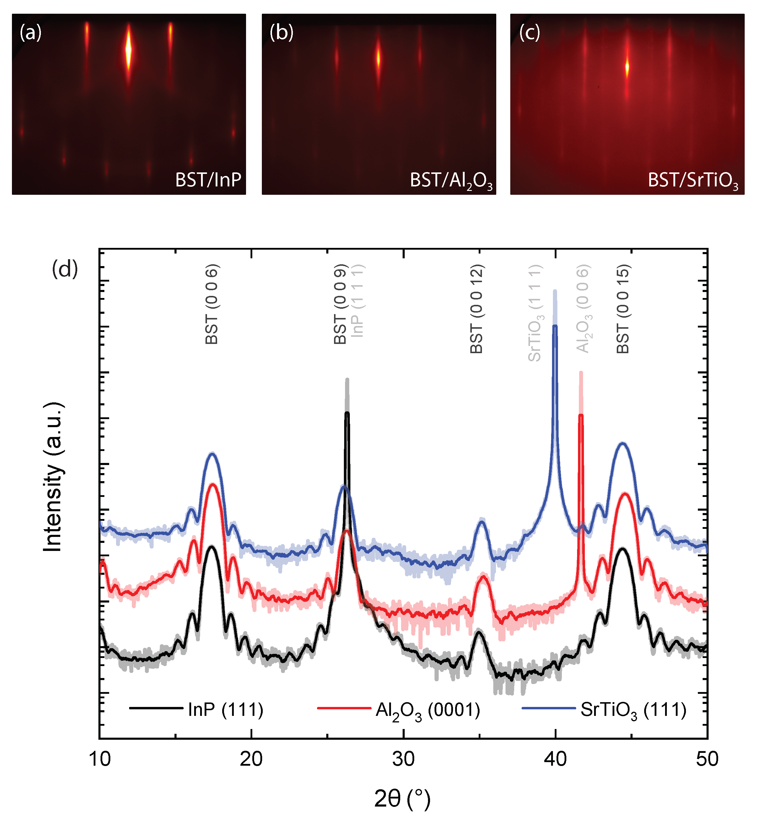
Abstract
:1. Introduction
2. Materials and Methods
3. Results and Discussion
3.1. Substrate and Material Choice
3.2. High Degree of Crystallinity, Consistent with vdW Epitaxy
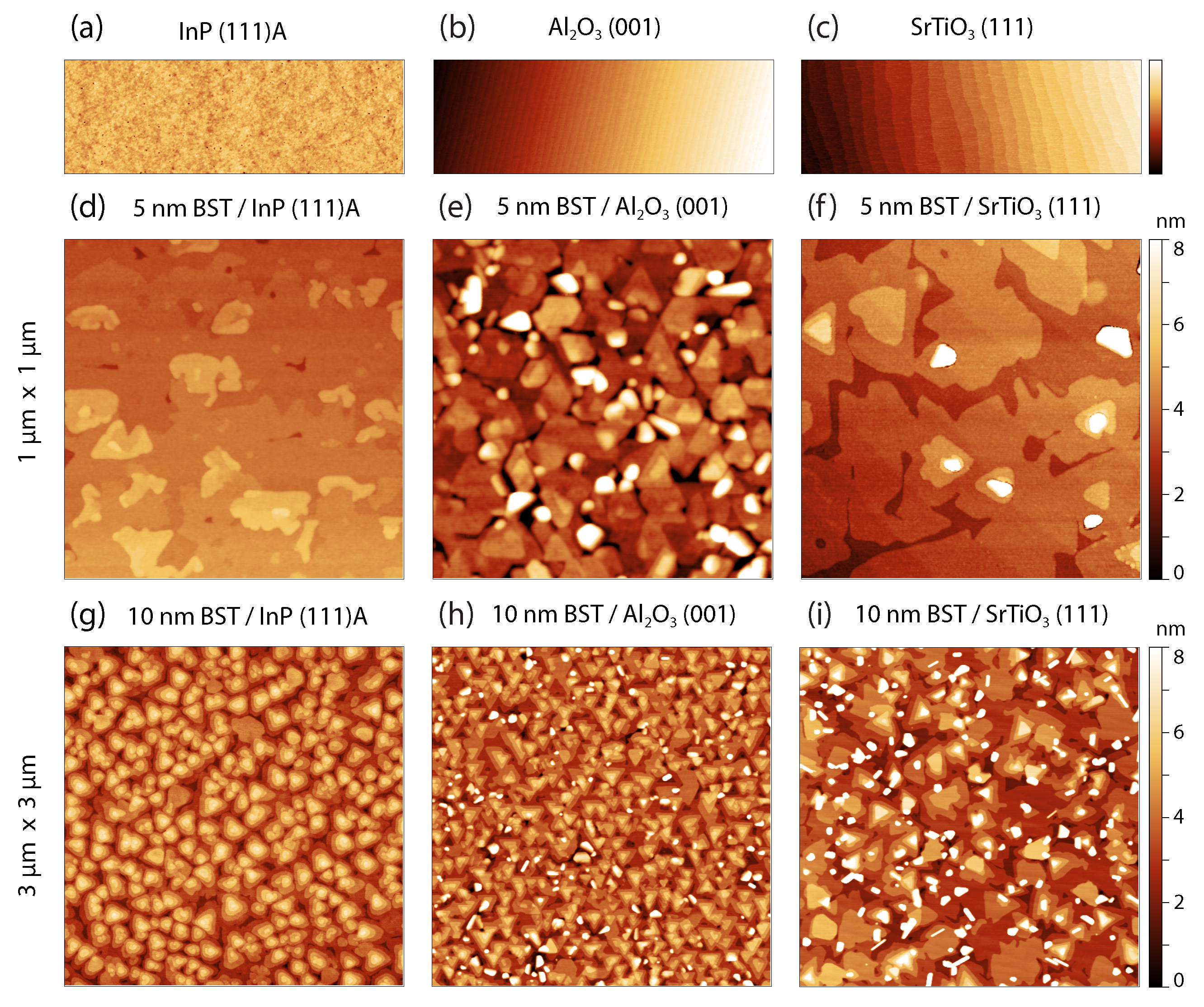
3.3. Morphological Differences, Indicating Quasi-vdW Epitaxy
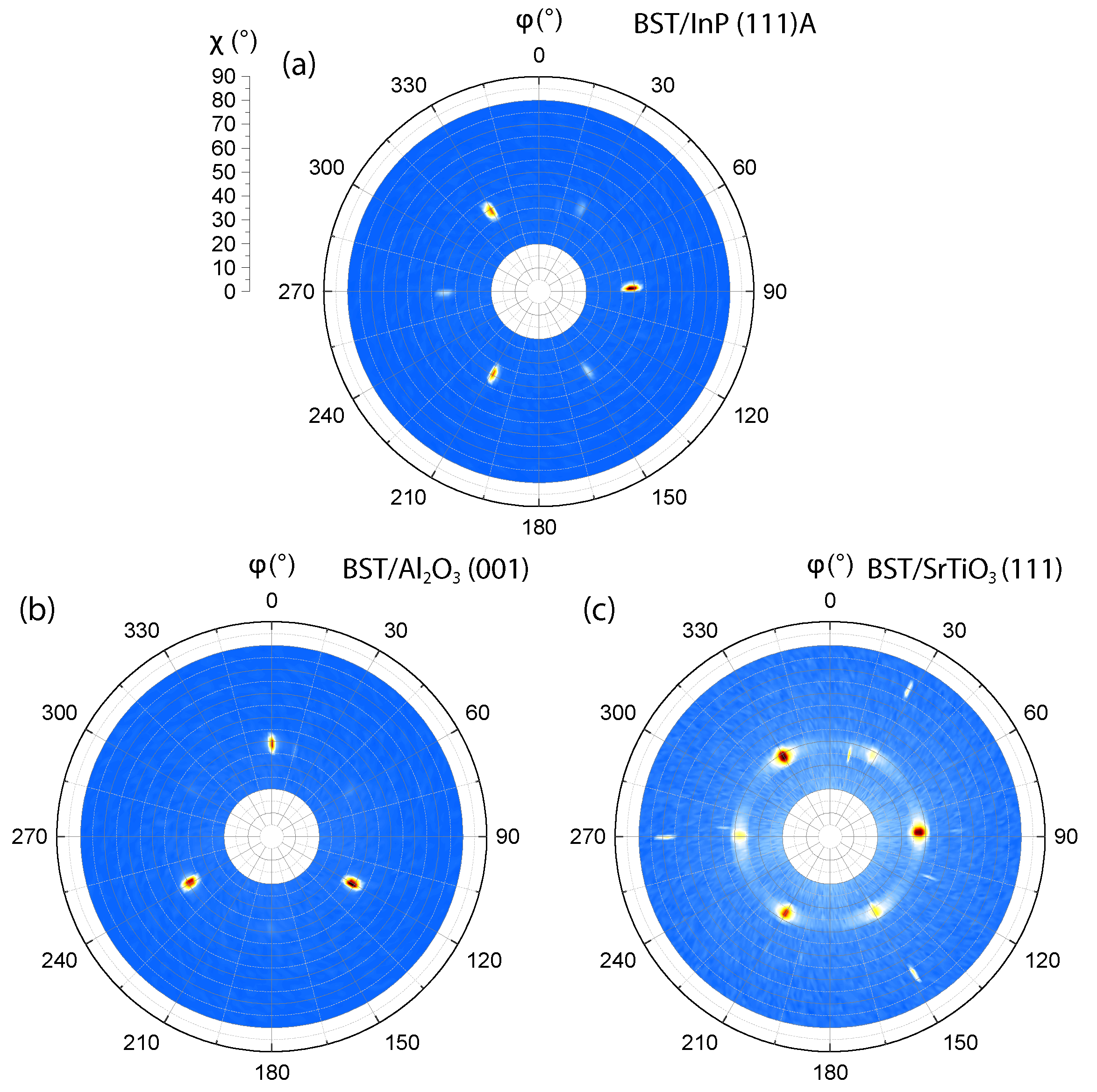
3.4. Employing Quasi-vdW Epitaxy to Enhance Single Domain Rotational Alignment with the Substrate
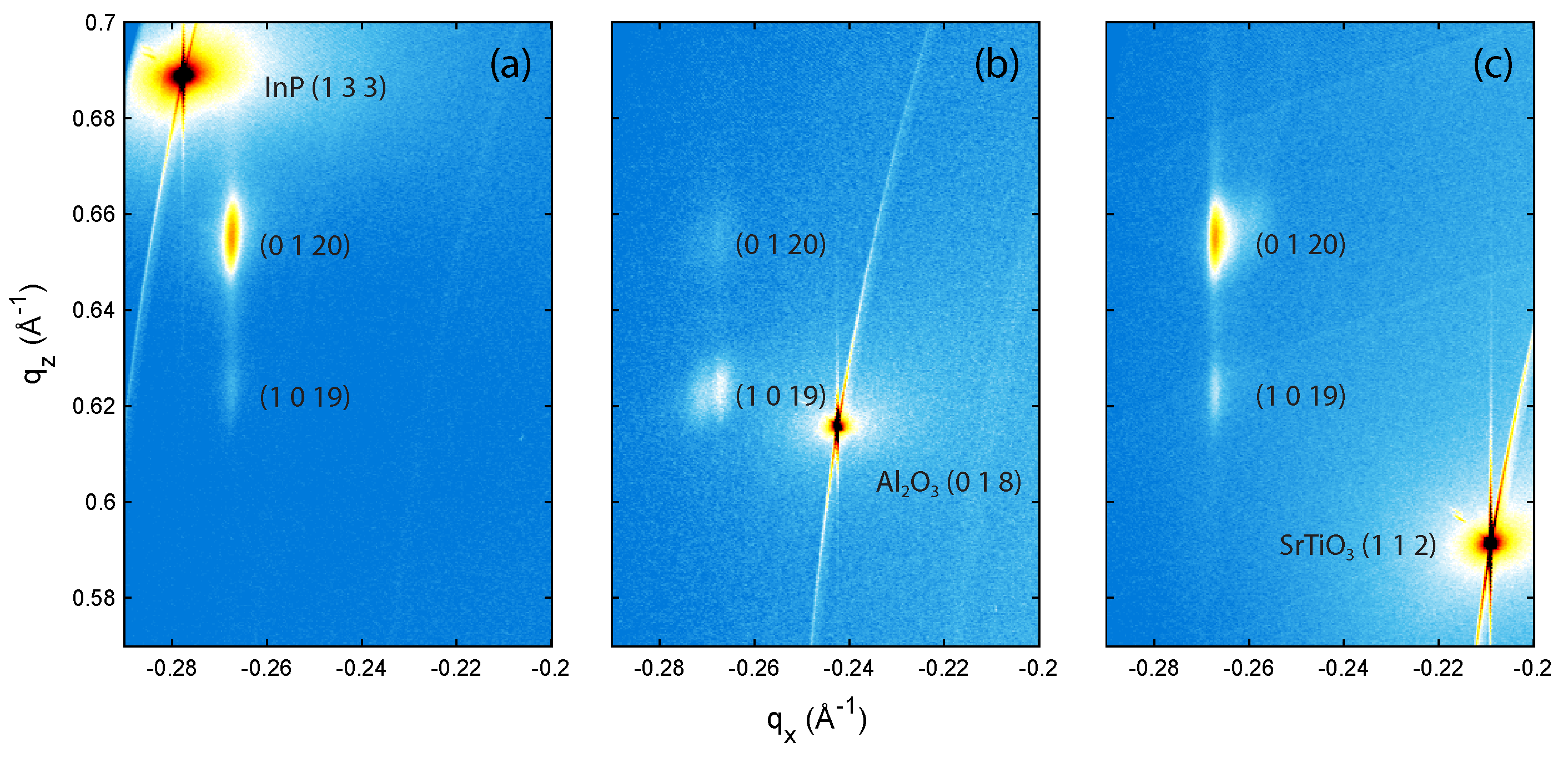
3.5. Revealing the Nature of the Film-Substrate Interaction in Quasi-vdW Epitaxy
4. Conclusions
Supplementary Materials
Author Contributions
Funding
Institutional Review Board Statement
Informed Consent Statement
Data Availability Statement
Acknowledgments
Conflicts of Interest
References
- Zhang, Y.; He, K.; Chang, C.Z.; Song, C.L.; Wang, L.L.; Chen, X.; Jia, J.F.; Fang, Z.; Dai, X.; Shan, W.Y.; et al. Crossover of the three-dimensional topological insulator Bi2Se3 to the two-dimensional limit. Nat. Phys. 2010, 6, 584–588. [Google Scholar] [CrossRef] [Green Version]
- Zhang, H.; Liu, C.X.; Qi, X.L.; Dai, X.; Fang, Z.; Zhang, S.C. Topological insulators in Bi2Se3, Bi2Te3 and Sb2Te3 with a single Dirac cone on the surface. Nat. Phys. 2009, 5, 438–442. [Google Scholar] [CrossRef]
- Xia, Y.; Qian, D.; Hsieh, D.; Wray, L.; Pal, A.; Lin, H.; Bansil, A.; Grauer, D.; Hor, Y.S.; Cava, R.J.; et al. Observation of a large-gap topological-insulator class with a single Dirac cone on the surface. Nat. Phys. 2009, 5, 398–402. [Google Scholar] [CrossRef] [Green Version]
- Hsieh, D.; Xia, Y.; Qian, D.; Wray, L.; Dil, J.H.; Meier, F.; Osterwalder, J.; Patthey, L.; Checkelsky, J.G.; Ong, N.P.; et al. A tunable topological insulator in the spin helical Dirac transport regime. Nature 2009, 460, 1101–1105. [Google Scholar] [CrossRef] [PubMed] [Green Version]
- Chen, Y.L.; Analytis, J.G.; Chu, J.H.; Liu, Z.K.; Mo, S.K.; Qi, X.L.; Zhang, H.J.; Lu, D.H.; Dai, X.; Fang, Z.; et al. Experimental realization of a three-dimensional topological insulator, Bi2Te3. Science 2009, 325, 178–181. [Google Scholar] [CrossRef] [Green Version]
- Hsieh, D.; Xia, Y.; Qian, D.; Wray, L.; Meier, F.; Dil, J.H.; Osterwalder, J.; Patthey, L.; Fedorov, A.V.; Lin, H.; et al. Observation of time-reversal-protected single-Dirac-cone topological-insulator states in Bi2Te3 and Sb2Te3. Phys. Rev. Lett. 2009, 103, 146401. [Google Scholar] [CrossRef] [Green Version]
- Fu, L.; Kane, C.L. Superconducting Proximity Effect and Majorana Fermions at the Surface of a Topological Insulator. Phys. Rev. Lett. 2008, 100, 096407. [Google Scholar] [CrossRef] [Green Version]
- Das Sarma, S.; Freedman, M.; Nayak, C. Majorana zero modes and topological quantum computation. npj Quantum Inf. 2015, 1, 15001. [Google Scholar] [CrossRef] [Green Version]
- Qi, X.L.; Li, R.; Zang, J.; Zhang, S.C. Inducing a Magnetic Monopole with Topological Surface States. Science 2009, 323, 1184–1187. [Google Scholar] [CrossRef] [Green Version]
- Nogueira, F.S.; Nussinov, Z.; van den Brink, J. Fractional Angular Momentum at Topological Insulator Interfaces. Phys. Rev. Lett. 2018, 121, 227001. [Google Scholar] [CrossRef] [Green Version]
- Zhang, J.; Chang, C.Z.; Zhang, Z.; Wen, J.; Feng, X.; Li, K.; Liu, M.; He, K.; Wang, L.; Chen, X.; et al. Band structure engineering in (Bi1−xSbx)2Te3 ternary topological insulators. Nat. Commun. 2011, 2, 574. [Google Scholar] [CrossRef] [PubMed] [Green Version]
- Richardella, A.; Kandala, A.; Lee, J.S.; Samarth, N. Characterizing the structure of topological insulator thin films. APL Mater. 2015, 3, 083303. [Google Scholar] [CrossRef] [Green Version]
- Ngabonziza, P. Quantum transport and potential of topological states for thermoelectricity in Bi2Te3 thin films. Nanotechnology 2022, 33, 192001. [Google Scholar] [CrossRef] [PubMed]
- Liu, W.; Endicott, L.; Stoica, V.A.; Chi, H.; Clarke, R.; Uher, C. High-quality ultra-flat BiSbTe3 films grown by MBE. J. Cryst. Growth 2015, 410, 23–29. [Google Scholar] [CrossRef] [Green Version]
- Yang, F.; Taskin, A.A.; Sasaki, S.; Segawa, K.; Ohno, Y.; Matsumoto, K.; Ando, Y. Top gating of epitaxial (Bi1−xSbx)2Te3 topological insulator thin films. Appl. Phys. Lett. 2014, 104, 161614. [Google Scholar] [CrossRef] [Green Version]
- He, L.; Kou, X.; Lang, M.; Choi, E.S.; Jiang, Y.; Nie, T.; Jiang, W.; Fan, Y.; Wang, Y.; Xiu, F.; et al. Evidence of the two surface states of (Bi0.53Sb0.47)2Te3 films grown by van der Waals epitaxy. Sci. Rep. 2013, 3, 3406. [Google Scholar] [CrossRef] [Green Version]
- Kim, K.C.; Lee, J.; Kim, B.K.; Choi, W.Y.; Chang, H.J.; Won, S.O.; Kwon, B.; Kim, S.K.; Hyun, D.B.; Kim, H.J.; et al. Free-electron creation at the 60° twin boundary in Bi2Te3. Nat. Commun. 2016, 7, 12449. [Google Scholar] [CrossRef] [Green Version]
- Shimizu, S.; Yoshimi, R.; Hatano, T.; Takahashi, K.S.; Tsukazaki, A.; Kawasaki, M.; Iwasa, Y.; Tokura, Y. Gate control of surface transport in MBE-grown topological insulator (Bi1−xSbx)2Te3 thin films. Phys. Rev. B 2012, 86, 045319. [Google Scholar] [CrossRef]
- Weyrich, C.; Drögeler, M.; Kampmeier, J.; Eschbach, M.; Mussler, G.; Merzenich, T.; Stoica, T.; Batov, I.E.; Schubert, J.; Plucinski, L.; et al. Growth, characterization, and transport properties of ternary (Bi1−xSbx)2Te3 topological insulator layers. J. Phys. Condens. Matter 2016, 28, 495501. [Google Scholar] [CrossRef] [Green Version]
- Zhang, G.; Qin, H.; Chen, J.; He, X.; Lu, L.; Li, Y.; Wu, K. Growth of topological insulator Bi2Se3 thin films on SrTiO3 with large tunability in chemical potential. Adv. Funct. Mater. 2011, 21, 2351–2355. [Google Scholar] [CrossRef]
- He, X.; Guan, T.; Wang, X.; Feng, B.; Cheng, P.; Chen, L.; Li, Y.; Wu, K. Highly tunable electron transport in epitaxial topological insulator (Bi1−xSbx)2Te3 thin films. Appl. Phys. Lett. 2012, 101, 123111. [Google Scholar] [CrossRef]
- He, X.; Li, H.; Chen, L.; Wu, K. Substitution-induced spin-splitted surface states in topological insulator (Bi1−xSbx)2Te3. Sci. Rep. 2015, 5, 8830. [Google Scholar] [CrossRef] [PubMed]
- Qin, H.; Guo, B.; Wang, L.; Zhang, M.; Xu, B.; Shi, K.; Pan, T.; Zhou, L.; Chen, J.; Qiu, Y.; et al. Superconductivity in single-quintuple-layer Bi2Te3 grown on epitaxial FeTe. Nano Lett. 2020, 20, 3160–3168. [Google Scholar] [CrossRef] [PubMed]
- Zhao, H.; Rachmilowitz, B.; Ren, Z.; Han, R.; Schneeloch, J.; Zhong, R.; Gu, G.; Wang, Z.; Zeljkovic, I. Superconducting proximity effect in a topological insulator using Fe(Te, Se). Phys. Rev. B 2018, 97, 224504. [Google Scholar] [CrossRef] [Green Version]
- Harrison, S.E.; Li, S.; Huo, Y.; Zhou, B.; Chen, Y.L.; Harris, J.S. Two-step growth of high quality Bi2Te3 thin films on Al2O3 (0001) by molecular beam epitaxy. Appl. Phys. Lett. 2013, 102, 171906. [Google Scholar] [CrossRef]
- Koirala, N.; Brahlek, M.; Salehi, M.; Wu, L.; Dai, J.; Waugh, J.; Nummy, T.; Han, M.G.; Moon, J.; Zhu, Y.; et al. Record Surface State Mobility and Quantum Hall Effect in Topological Insulator Thin Films via Interface Engineering. Nano Lett. 2015, 15, 8245–8249. [Google Scholar] [CrossRef]
- Wang, Y.; Ginley, T.P.; Law, S. Growth of high-quality Bi2Se3 topological insulators using (Bi1−xInx)2Se3 buffer layers. J. Vac. Sci. Technol. B 2018, 36, 02D101. [Google Scholar] [CrossRef]
- Wang, Z.; Li, H.; Guo, X.; Ho, W.; Xie, M. Growth characteristics of topological insulator Bi2Se3 films on different substrates. J. Cryst. Growth 2011, 334, 96–102. [Google Scholar] [CrossRef]
- Hwang, J.Y.; Kim, Y.M.; Lee, K.H.; Ohta, H.; Kim, S.W. Te monolayer-driven spontaneous van der Waals epitaxy of two-dimensional pnictogen chalcogenide film on sapphire. Nano Lett. 2017, 17, 6140–6145. [Google Scholar] [CrossRef]
- Walsh, L.A.; Hinkle, C.L. Van der Waals epitaxy: 2D materials and topological insulators. Appl. Mater. Today 2017, 9, 504–515. [Google Scholar] [CrossRef]
- Nečas, D.; Klapetek, P. Gwyddion: An open-source software for SPM data analysis. Cent. Eur. J. Phys. 2012, 10, 181–188. [Google Scholar] [CrossRef]
- Degen, T.; Sadki, M.; Bron, E.; König, U.; Nénert, G. The HighScore Suite. Powder Diffr. 2014, 29, S13–S18. [Google Scholar] [CrossRef] [Green Version]
- Yang, F.; Taskin, A.A.; Sasaki, S.; Segawa, K.; Ohno, Y.; Matsumoto, K.; Ando, Y. Dual-gated topological insulator thin-film device for efficient fermi-level tuning. ACS Nano 2015, 9, 4050–4055. [Google Scholar] [CrossRef] [PubMed]
- Li, B.; Guo, X.; Ho, W.; Xie, M. Strain in epitaxial Bi2Se3 grown on GaN and graphene substrates: A reflection high-energy electron diffraction study. Appl. Phys. Lett. 2015, 107, 081604. [Google Scholar] [CrossRef] [Green Version]
- Tarakina, N.V.; Schreyeck, S.; Luysberg, M.; Grauer, S.; Schumacher, C.; Karczewski, G.; Brunner, K.; Gould, C.; Buhmann, H.; Dunin-Borkowski, R.E.; et al. Suppressing twin formation in Bi2Se3 thin films. Adv. Mater. Interfaces 2014, 1, 1400134. [Google Scholar] [CrossRef] [Green Version]
- Borisova, S.; Krumrain, J.; Luysberg, M.; Mussler, G.; Grützmacher, D. Mode of growth of ultrathin topological insulator Bi2Te3 films on Si (111) substrates. Cryst. Growth Des. 2012, 12, 6098–6103. [Google Scholar] [CrossRef]
- Borisova, S.; Kampmeier, J.; Luysberg, M.; Mussler, G.; Grützmacher, D. Domain formation due to surface steps in topological insulator Bi2Te3 thin films grown on Si (111) by molecular beam epitaxy. Appl. Phys. Lett. 2013, 103, 081902. [Google Scholar] [CrossRef] [Green Version]
- Lanius, M.; Kampmeier, J.; Kölling, S.; Mussler, G.; Koenraad, P.M.; Grützmacher, D. Topography and structure of ultrathin topological insulator Sb2Te3 films on Si(111) grown by means of molecular beam epitaxy. J. Cryst. Growth 2016, 453, 158–162. [Google Scholar] [CrossRef]
- Winnerlein, M.; Schreyeck, S.; Grauer, S.; Rosenberger, S.; Fijalkowski, K.M.; Gould, C.; Brunner, K.; Molenkamp, L.W. Epitaxy and structural properties of (V,Bi,Sb)2Te3 layers exhibiting the quantum anomalous Hall effect. Phys. Rev. Mater. 2017, 1, 011201(R). [Google Scholar] [CrossRef] [Green Version]
- Mu, X.; Zhou, H.; He, D.; Zhao, W.; Wei, P.; Zhu, W.; Nie, X.; Liu, H.; Zhang, Q. Enhanced electrical properties of stoichiometric Bi0.5Sb1.5Te3 film with high-crystallinity via layer-by-layer in-situ growth. Nano Energy 2017, 33, 55–64. [Google Scholar] [CrossRef]
- Kandala, A. Transport Studies of Mesoscopic and Magnetic Topological Insulators. Ph.D. Thesis, Pennsylvania State University, State College, PA, USA, 2015. [Google Scholar]
- Kremer, G.; Zhu, K.; Pierron, T.; Fournee, V.; Ledieu, J.; Andrieu, S.; Kierren, B.; Moreau, L.; Malterre, D.; He, K.; et al. Recovery of surface state bands after desorption of Te capping layer on (Bi1−xSbx)2Te3 ternary topological insulators. J. Phys. D Appl. Phys. 2019, 52, 494002. [Google Scholar] [CrossRef]
- Ferhat, M.; Tedenac, J.C.; Nagao, J. Mechanisms of spiral growth in Bi2Te3 thin films grown by the hot-wall-epitaxy technique. J. Cryst. Growth 2000, 218, 250–258. [Google Scholar] [CrossRef]
- Gilmer, G.H.; Grabow, M.H. Models of thin film growth modes. J. Met. 1987, 39, 19–23. [Google Scholar] [CrossRef]
- Guo, X.; Xu, Z.J.; Liu, H.C.; Zhao, B.; Dai, X.Q.; He, H.T.; Wang, J.N.; Liu, H.J.; Ho, W.K.; Xie, M.H. Single domain Bi2Se3 films grown on InP(111)A by molecular-beam epitaxy. Appl. Phys. Lett. 2013, 102, 151604. [Google Scholar] [CrossRef] [Green Version]
- Richardson, C.L.; Devine-Stoneman, J.M.; Divitini, G.; Vickers, M.E.; Chang, C.Z.; Amado, M.; Moodera, J.S.; Robinson, J.W.A. Structural properties of thin-film ferromagnetic topological insulators. Sci. Rep. 2017, 7, 12061. [Google Scholar] [CrossRef] [Green Version]
- Lanius, M.; Kampmeier, J.; Weyrich, C.; Kölling, S.; Schall, M.; Schüffelgen, P.; Neumann, E.; Luysberg, M.; Mussler, G.; Koenraad, P.M.; et al. P–N junctions in ultrathin topological insulator Sb2Te3/Bi2Te3 heterostructures grown by molecular beam epitaxy. Cryst. Growth Des. 2016, 16, 2057–2061. [Google Scholar] [CrossRef]
- Reed, T.B. Free Energy of Formation of Binary Compounds: An Atlas of Charts for High-Temperature Chemical Calculations; MIT Press: Cambridge, MA, USA, 1971. [Google Scholar]
- Volykhov, A.A.; Sánchez-Barriga, J.; Batuk, M.; Callaert, C.; Hadermann, J.; Sirotina, A.P.; Neudachina, V.S.; Belova, A.I.; Vladimirova, N.V.; Tamm, M.E.; et al. Can surface reactivity of mixed crystals be predicted from their counterparts? A case study of (Bi1−xSbx)2Te3 topological insulators. J. Mater. Chem. C 2018, 6, 8941–8949. [Google Scholar] [CrossRef] [Green Version]
- Koster, G.; Kropman, B.L.; Rijnders, G.J.H.M.; Blank, D.H.A.; Rogalla, H. Quasi-ideal strontium titanate crystal surfaces through formation of strontium hydroxide. Appl. Phys. Lett. 1998, 73, 2920–2922. [Google Scholar] [CrossRef] [Green Version]
- Kampmeier, J.; Borisova, S.; Plucinski, L.; Luysberg, M.; Mussler, G.; Grützmacher, D. Suppressing twin domains in molecular beam epitaxy grown Bi2Te3 topological insulator thin films. Cryst. Growth Des. 2015, 15, 390–394. [Google Scholar] [CrossRef]
- Mussler, G. Molecular-beam epitaxy of 3D topological insulator thin films and devices on Si substrates. Phys. Status Solidi B 2021, 258, 2000007. [Google Scholar] [CrossRef]
- Ginley, T.P.; Wang, Y.; Law, S. Topological insulator film growth by molecular beam epitaxy: A review. Crystals 2016, 6, 154. [Google Scholar] [CrossRef]
- Bouwmeester, R.L.; de Hond, K.; Gauquelin, N.; Verbeeck, J.; Koster, G.; Brinkman, A. Stabilization of the Perovskite Phase in the Y–Bi–O System By Using a BaBiO3 Buffer Layer. Phys. Status Solidi (RRL)—Rapid Res. Lett. 2019, 13, 1800679. [Google Scholar] [CrossRef] [Green Version]


Publisher’s Note: MDPI stays neutral with regard to jurisdictional claims in published maps and institutional affiliations. |
© 2022 by the authors. Licensee MDPI, Basel, Switzerland. This article is an open access article distributed under the terms and conditions of the Creative Commons Attribution (CC BY) license (https://creativecommons.org/licenses/by/4.0/).
Share and Cite
Mulder, L.; Wielens, D.H.; Birkhölzer, Y.A.; Brinkman, A.; Concepción, O. Revisiting the van der Waals Epitaxy in the Case of (Bi0.4Sb0.6)2Te3 Thin Films on Dissimilar Substrates. Nanomaterials 2022, 12, 1790. https://0-doi-org.brum.beds.ac.uk/10.3390/nano12111790
Mulder L, Wielens DH, Birkhölzer YA, Brinkman A, Concepción O. Revisiting the van der Waals Epitaxy in the Case of (Bi0.4Sb0.6)2Te3 Thin Films on Dissimilar Substrates. Nanomaterials. 2022; 12(11):1790. https://0-doi-org.brum.beds.ac.uk/10.3390/nano12111790
Chicago/Turabian StyleMulder, Liesbeth, Daan H. Wielens, Yorick A. Birkhölzer, Alexander Brinkman, and Omar Concepción. 2022. "Revisiting the van der Waals Epitaxy in the Case of (Bi0.4Sb0.6)2Te3 Thin Films on Dissimilar Substrates" Nanomaterials 12, no. 11: 1790. https://0-doi-org.brum.beds.ac.uk/10.3390/nano12111790