Empirical Equation Based Chirality (n, m) Assignment of Semiconducting Single Wall Carbon Nanotubes from Resonant Raman Scattering Data

Abstract
:1. Introduction
2. ModifiedTight Binding Model

 , and n is an integer. This equation gives first optical transition energy for i = 1, j =1,


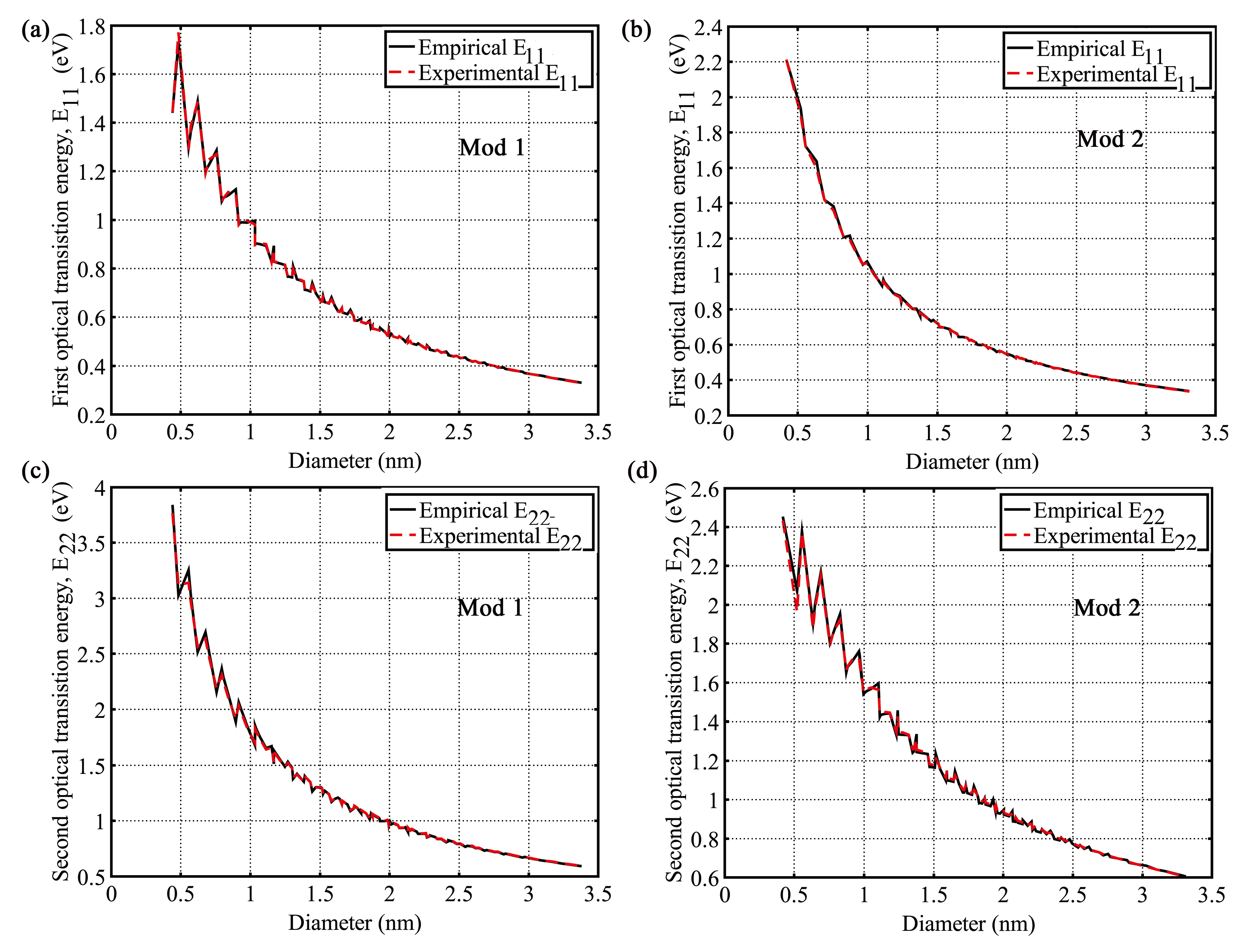
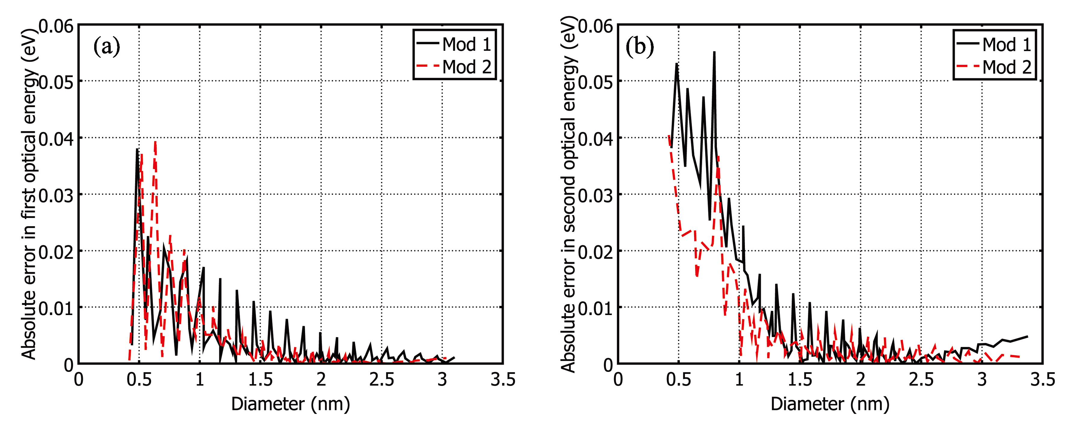
| MOD 1 Type | MOD 2 Type | |||
|---|---|---|---|---|
| Diameter, dt (nm) | Average | Average | Average | Average |
| | Δ E | | % | Δ E | | | Δ E | | % | Δ E | | |
| 0.4 ≤ dt ≤ 3.0 | 0.0036 | 0.43% | 0.0033 | 0.32% |
| 1.0 ≤ dt ≤ 3.0 | 0.0023 | 0.36% | 0.0015 | 0.20% |
| 1.5 ≤ dt ≤ 3.0 | 0.0015 | 0.29% | 0.0006 | 0.11% |
| MOD 1 Type | MOD 2 Type | |||
|---|---|---|---|---|
| Diameter, dt (nm) | Average | Average | Average | Average |
| | ΔE | | % | ΔE | | | ΔE | | % | ΔE | | |
| 0.4 ≤ dt ≤ 3.0 | 0.0115 | 0.66% | 0.0083 | 0.57% |
| 1.0 ≤ dt ≤ 3.0 | 0.0052 | 0.46% | 0.0037 | 0.35% |
| 1.5 ≤ dt ≤ 3.0 | 0.0037 | 0.39% | 0.0031 | 0.33% |
3. Method
 and
and  , respectively. From Equations (20) and (21), the values of and can be expressed as


 and
and  , respectively. From Equations (18) and (19), corresponding values of and are

 , ) and ( , ), which are the candidates for chiral index of unknown SWCNT.
  and
and  , respectively. From Equations (24) and (25), the values of and can be expressed as


 and
and  , respectively. From Equations (22) and (23), corresponding values of and are

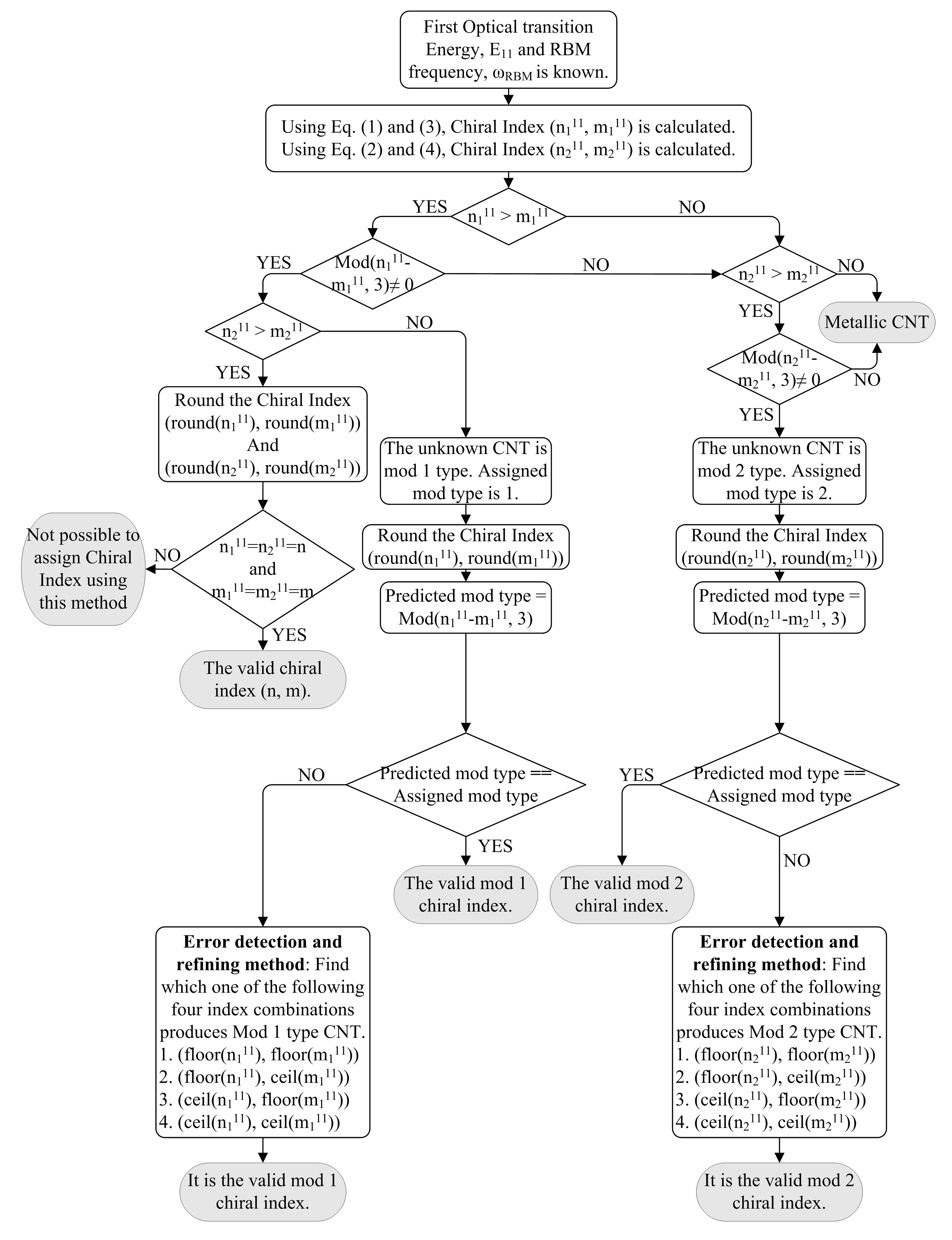
 and and corresponding and may become fractions. Finally, Equations (12)-(15) give two pairs ( , ) and ( , ) that are the candidates for chiral index of unknown SWCNT. , ) and ( , ) are calculated from Equations (8)-(11). The pair ( , ) originates from mod 1 type’s equation, whereas the pair ( , ) originates from mod 2 type’s equation. > and < , assigned mod type is mod 1. Rounding the pair ( , ), the predicted mod type is calculated using mod(round( ) − round( ), 3). If the assigned mod type is same as the predicted mod type, the rounded pair gives the actual mod 1 type chiral index. If the assigned mod type is not equal to the predicted mod type, error detection and refining method is applied on the ( , ) pair. Second, assigned mod type is mod 2 if < and > . The predicted mod type is calculated using mod( − , 3) after rounding the pair ( , ).The rounded pair gives the actual mod 2 type chiral index if the assigned mod type is same as the predicted mod type. If the assigned mod type is not equal to the predicted mod type, error detection and refining method is applied on the ( , ) pair. Third, for > and > conditions, if rounding to nearest interger results round( ) = round( ) = n and round( ) = round( ) = m, the chirality of the unknown CNT is (n, m). Otherwise, the chirality of that unknown CNT cannot be determined. Finally, though the empirical equations are formulated for mod 1 and mod 2 SWCNT, it can be extended for metallic CNTs only to detect. If the unknown CNT is metallic rather than SWCNT, the values of ( , ) and ( , ) pairs follow the condition: < and < . Since both conditions fail to satisfy the condition of semiconducting SWCNT, the sample is a metallic CNT. This condition is particularly useful to detect the presence of metallic CNT as clean separation of metallic CNT from semiconducting CNT is experimentally difficult.
  ), floor( )), (floor( ), ceil( )), (ceil( ), floor( )), and (ceil( ), ceil( )). From this list, the one that matches with assigned mod type (mod 1) is reassigned as the true chiral index of that semiconducting SWCNT. Similarly, possible chiral index pairs for mod 2 are listed as four combinations and one pair is reassigned as true chiral index that matches with assigned mod type (mod 2). , ) and ( , ) are calculated from Equations (12)-(15). > and > satisfy, but the conditions round( ) = round( ) and round( ) = round( ) do not satisfy, the chirality of that CNT cannot be determined using this algorithm. In this situation, alternate optical transition energy information may determine the actual chirality.
 4. Results
> and < (mod 1) or > and < (mod 2), while two of them satisfy round( ) = round( ) and round( ) = round( ) conditions. The remaining four semiconducting SWCNTs are further treated using error detection and refining method. For example, consider the actual chirality of (7, 3) whose (n, m) pairs are calculated as (6.7, 3.37) and (4.85, 5.4). Since these pairs satisfy the conditions > and < , the assigned mod type and the predicted chirality after rounding is 1 and (7, 3), respectively. The assigned mod type is the same as the predicted mod type (calculated from predicted chirality) in this case. Therefore, the mod type and chirality is 1 and (7, 3), respectively. Next, consider the actual chirality of (5, 4). The (n, m) pairs for mod 1 and mod 2 calculated from the empirical equations are (5.01, 3.99) and (4.83, 4.18), respectively. As rounding the values gives same pair, the assigned chirality is (5, 4). Lastly, consider the case where error detection and refining method is necessary. For the actual chirality of (13, 2), the (n, m) pairs are calculated as (8.17, 8.22) and (12.73, 2.57). These pairs satisfy the conditions < and > , and consequently, the assigned mod type and the predicted chirality after rounding is 2 and (13, 3), respectively. Here, the assigned mod type is not the same as the predicted mod type (calculated from predicted chirality) in this case. The values that have fraction parts of n and m within 0.40 to 0.60, are prone to wrong assignment due to the error margin of our empirical equations or due to slight deviation in experimental data. Therefore, the valid pair is in the close vicinity of the actual chiral index. From the four possible nearest integer pairs, (12, 2), (12, 3), (13, 2), and (13,3), only (13,2) is mod 2 type. Therefore, (13, 2), which has the same mod type as the assigned mod type, is considered as the correct chiral index of that SWCNT. Following the presented algorithm, all 28 semiconducting SWCNTs were properly assigned with their actual chiral index from E11 and ωrbm. > and < (mod 1) or > and < (mod 2), while four of them satisfy round( ) = round( ) and round( ) = round( ) conditions. The remaining three semiconducting SWCNTs are further treated using error detection and refining method. Similar algorithm is applied to determine the actual chiral index from E22 and ωrbm. | RRS Data | (n, m) pair for mod 1a | (n, m) pair for mod 2b | Predicted chiralityc | Predi--ctedd | Assi--gnede | Re-assi--gnedf | Actual chiral | |||
| ωrbm (cm−1) | E11 (ev) | | | | | (n, m) | Mod | Mod | Chirality | (n, m) |
| 373.0 [50] | 1.488 [50] | 5.01 | 3.99 | 4.83 | 4.18 | (5, 4) | 1 | 1 | (5, 4) | |
| 335.2 [50] | 1.420 [50] | 5.28 | 4.79 | 6.03 | 3.97 | (6, 4) | 2 | 2 | (6, 4) | |
| 329.5 [43] | 1.249 [43] | 6.7 | 3.37 | 4.85 | 5.4 | (7, 3) | 1 | 1 | (7, 3) | |
| 309.0 [43] | 1.283 [43] | 6.04 | 4.9 | 5.97 | 4.98 | (6, 5) | 1 | 1 | (6, 5) | |
| 304.0 [34] | 1.362 [43] | 5.5 | 5.65 | 8.84 | 1.47 | (9, 1) | 2 | 2 | (9, 1) | |
| 297.0 [43] | 1.306 [43] | 5.78 | 5.64 | 7.78 | 3.36 | (8, 3) | 2 | 2 | (8, 3) | |
| 291.0 [38] | 1.100 [43] | 8.75 | 2.32 | 5.28 | 6.37 | (9, 2) | 1 | 1 | (9, 2) | |
| 283.0 [50] | 1.212 [50] | 6.39 | 5.62 | 7.01 | 4.95 | (7, 5) | 2 | 2 | (7, 5) | |
| 280.0 [42] | 1.110 [35] | 7.85 | 4.11 | 5.79 | 6.36 | (8, 4) | 1 | 1 | (8, 4) | |
| 263.0 [50] | 1.117 [50] | 6.49 | 6.48 | 9.75 | 2.54 | (10, 3) | 1 | 2 | (10, 2) | (10, 2) |
| 264.0 [43] | 1.110 [43] | 7.26 | 5.63 | 7.87 | 6.05 | (7, 6) | 1 | 1 | (7, 6) | |
| 256.0 [37] | 0.982 [50] | 11.23 | 0.63 | 5.91 | 7.42 | (11, 1) | 1 | 1 | (11, 1) | |
| 256.8 [43] | 1.140 [43] | 6.73 | 6.57 | 9.22 | 3.7 | (9, 4) | 2 | 2 | (9, 4) | |
| 251.0 [50] | 0.992 [50] | 9.85 | 3.24 | 6.23 | 7.38 | (10, 3) | 1 | 1 | (10, 3) | |
| 246.4 [39] | 1.060 [35] | 7.53 | 6.35 | 7.84 | 6.02 | (8, 6) | 2 | 2 | (8, 6) | |
| 242.0 [42] | 0.997 [50] | 8.77 | 5.25 | 6.91 | 7.25 | (9, 5) | 1 | 1 | (9, 5) | |
| 231.8 [42] | 1.036 [50] | 7.46 | 7.35 | 10.67 | 3.58 | (11, 4) | 1 | 2 | (11, 3) | (11, 3) |
| 229.0 [34] | 0.979 [50] | 8.41 | 6.57 | 8.04 | 6.96 | (8, 7) | 1 | 1 | (8, 7) | |
| 226.0 [42] | 0.901 [50] | 11.89 | 2.29 | 6.82 | 8.37 | (12, 2) | 1 | 1 | (12, 2) | |
| 221.8 [37] | 0.904 [50] | 10.74 | 4.34 | 7.19 | 8.32 | (11, 4) | 1 | 1 | (11, 4) | |
| 215.0 [50] | 0.937 [50] | 8.63 | 7.41 | 9.25 | 6.73 | (9, 7) | 2 | 2 | (9, 7) | |
| 213.4 [50] | 0.898 [50] | 9.81 | 6.24 | 8.01 | 8.17 | (10, 6) | 1 | 1 | (10, 6) | |
| 210.9 [50] | 0.949 [50] | 8.17 | 8.22 | 12.73 | 2.57 | (13, 3) | 1 | 2 | (13, 2) | (13, 2) |
| 206.0 [34] | 0.924 [50] | 8.43 | 8.37 | 12.47 | 3.51 | (12, 4) | 2 | 2 | (12, 4) | |
| 203.3 [39] | 0.828 [50] | 12.97 | 3.08 | 7.67 | 9.34 | (13, 3) | 1 | 1 | (13, 3) | |
| 198.5 [39] | 0.829 [50] | 11.43 | 5.73 | 8.27 | 9.2 | (11, 6) | 2 | 1 | (12, 5) | (12, 5) |
| 192.5 [50] | 0.841 [50] | 9.78 | 8.25 | 10.27 | 7.73 | (10, 8) | 2 | 2 | (10, 8) | |
| 187.2 [50] | 0.835 [50] | 9.49 | 9.12 | 12.82 | 5.26 | (13, 5) | 2 | 2 | (13, 5) | |
, ) pair and ( , ) pair, the assigned mod type is mod 1 and mod 2, respectively; f If the predicted mod type and assigned mod type is not same, chiral index is selected from four index combination using error detection and refining method. < and < , the sample is detected as metallic CNTs. | RRS Data | (n, m) pair for mod 1a | (n, m) pair for mod 2b | Predicted chiralityc | Predi--ctedd | Assi--gnede | Re-assi--gnedf | Actual chiral | |||
| ωrbm (cm−1) | E22 (ev) | | | | | (n, m) | Mod | Mod | Chirality | (n, m) |
| 309.0 [38] | 2.180 [38] | 6.01 | 4.94 | 5.44 | 5.52 | (6, 5) | 1 | 1 | (6, 5) | |
| 304.0 [34] | 1.800 [42] | 5.07 | 6.07 | 9.22 | 0.83 | (9, 1) | 2 | 2 | (9, 1) | |
| 299.0 [38] | 1.860 [38] | 5.33 | 6.03 | 7.71 | 3.35 | (8, 3) | 2 | 2 | (8, 3) | |
| 283.0 [50] | 1.920 [42] | 6.01 | 6.01 | 6.69 | 5.34 | (7, 5) | 2 | 2 | (7, 5) | |
| 278.8 [43] | 2.110 [42] | 7.62 | 4.45 | 5.69 | 6.51 | (8, 4) | 1 | 1 | (8, 4) | |
| 264.6 [39] | 1.690 [39] | 5.93 | 6.95 | 9.98 | 2.09 | (10, 2) | 2 | 2 | (10, 2) | |
| 264.2 [37] | 1.910 [37] | 6.98 | 5.92 | 6.54 | 6.38 | (7, 6) | 1 | 1 | (7, 6) | |
| 257.5 [39] | 1.720 [39] | 6.31 | 6.95 | 8.55 | 4.51 | (9, 5) | 1 | 2 | (9, 4) | (9, 4) |
| 245.0 [42] | 1.720 [42] | 6.98 | 6.99 | 7.92 | 6.02 | (8, 6) | 2 | 2 | (8, 6) | |
| 242.0 [42] | 1.850 [42] | 8.66 | 5.37 | 6.69 | 7.46 | (9, 5) | 1 | 1 | (9, 5) | |
| 236.0 [50] | 1.556 [50] | 6.65 | 7.88 | 12.24 | 0.69 | (12, 1) | 2 | 2 | (12, 1) | |
| 233.0 [50] | 1.565 [50] | 6.84 | 7.89 | 11.04 | 2.95 | (11, 3) | 2 | 2 | (11, 3) | |
| 230.0 [42] | 1.700 [42] | 8.08 | 6.85 | 7.63 | 7.31 | (8, 7) | 1 | 1 | (8, 7) | |
| 227.0 [50] | 1.820 [37] | 11.88 | 2.21 | 6.76 | 8.37 | (12, 2) | 1 | 1 | (12, 2) | |
| 226.0 [46] | 1.570 [46] | 7.29 | 7.93 | 9.77 | 5.22 | (10, 5) | 2 | 2 | (10, 5) | |
| 221.8 [37] | 1.760 [37] | 11.16 | 3.77 | 7.04 | 8.47 | (11, 4) | 1 | 1 | (11, 4) | |
| 216.0 [39] | 1.564 [39] | 8.20 | 7.74 | 8.68 | 7.25 | (9, 7) | 2 | 2 | (9, 7) | |
| 212.0 [42] | 1.640 [50] | 9.98 | 6.16 | 7.74 | 8.55 | (10, 6) | 1 | 1 | (10, 6) | |
| 207.1 [46] | 1.447 [46] | 7.85 | 8.85 | 11.9 | 4.21 | (12, 4) | 2 | 2 | (12, 4) | |
| 204.0 [37] | 1.535 [37] | 9.36 | 7.65 | 8.64 | 8.39 | (9, 8) | 1 | 1 | (9, 8) | |
| 203.0 [42] | 1.620 [42] | 12.49 | 3.83 | 7.73 | 9.31 | (12, 4) | 2 | 1 | (13, 3) | (1, 3) |
| 200.0 [34] | 1.440 [34] | 8.45 | 8.88 | 10.66 | 6.51 | (11, 7) | 1 | 2 | (11, 6) | (11, 6) |
| 197.7 [46] | 1.560 [46] | 11.73 | 5.44 | 8.12 | 9.42 | (12, 5) | 1 | 1 | (12, 5) | |
| 192.5 [50] | 1.428 [50] | 9.28 | 8.78 | 9.94 | 8.08 | (10, 8) | 2 | 2 | (10, 8) | |
| 189.3 [46] | 1.479 [46] | 11.42 | 6.77 | 8.72 | 9.66 | (11, 7) | 1 | 1 | (11, 7) | |
| 183.0 [34] | 1.466 [34] | 14.14 | 4.00 | 8.63 | 10.40 | (14, 4) | 1 | 1 | (14, 4) | |
| 183.3 [50] | 1.390 [50] | 10.27 | 8.74 | 9.88 | 9.15 | (10, 9) | 1 | 1 | (10, 9) | |
, ) pair and ( , ) pair, the assigned mod type is mod 1 and mod 2, respectively; f If the predicted mod type and assigned mod type is not same, chiral index is selected from four index combination using error detection and refining method.5. Conclusions
Appendix
A. Chirality Assignment from First Optical Transition Energy

 , we get,


 and , respectively. Solving Equations (17) and (18) for gives
 gives
gives
 and gives two values for (+) and (−) terms. The values of and corresponding to the (−) terms of the above two expressions were always found to give negative value and hence become invalid as the chirality index (n and m) cannot be negative. So, only the values of and corresponding to the (+) terms can be taken for consideration. and are = 2 - a1 and = 2 - a2, respectively. As the values of and and the corresponding and may become fractions, they are rounded to nearest integers. These give two integer pairs ( , ) and ( , ) who are the candidates for chiral index of unknown SWCNT.
B. Chirality assignment from Second Optical Transition Energy

 and , respectively. Solving Equations (17) and (22) for gives
 gives
gives
 and gives two values for the (+) and (−) terms. Just like before, the values of and corresponding to the (−) terms of the above two expressions were always found to give negative value and become invalid. Only the values of and corresponding to the (+) terms can be taken. and are = 2 - b1 and = 2 - b2, respectively. As the values of and and the corresponding and may become fractions, they are rounded to nearest integers. These give two integer pairs ( , ) and ( , ) who are the candidates for chiral index of unknown SWCNT.
References
- Chen, C.X.; Lu, Y.; Kong, E.S.; Zhang, Y.F.; Lee, S.T. Nanowelded carbon-nanotube-based solar microcells. Small 2008, 4, 1313–1318. [Google Scholar] [CrossRef]
- Lee, J.U. Photovoltaic effect in ideal carbon nanotube diodes. Appl. Phys. Lett. 2005, 87, 073101. [Google Scholar] [CrossRef]
- Lu, S.; Panchapakesan, B. Photoconductivity in single wall carbon nanotube sheets. Nanotechnology 2006, 17, 1843–1850. [Google Scholar] [CrossRef]
- Blackburn, J.L.; Barnes, T.M.; Beard, M.C.; Kim, Y.H.; Tenent, R.C.; McDonald, T.J.; To, B.; Coutts, T.J.; Heben, M.J. Transparent conductive single-walled carbon nanotube networks with precisely tunable ratios of semiconducting and metallic nanotubes. ACS Nano. 2008, 2, 1266–1274. [Google Scholar]
- Bindl, D.J.; Arnold, M.S. Semiconducting carbon nanotube photovoltaic photodetectors. Int. J. High Speed Electron. Syst. 2011, 20, 687. [Google Scholar] [CrossRef]
- Bindl, D.J.; Safron, N.S.; Arnold, M.S. Dissociating excitons photogenerated in semiconducting carbon nanotubes at polymeric photovoltaic heterojunction interfaces. ACS Nano. 2010, 4, 5657–5664. [Google Scholar] [CrossRef]
- Avouris, P.; Freitag, M.; Perebeinos, V. Carbon-nanotube photonics and optoelectronics. Nat. Photon. 2008, 2, 341–350. [Google Scholar] [CrossRef]
- Avouris, P.; Chen, J. Nanotube electronics and optoelectronics. Mater. Today 2006, 9, 46–54. [Google Scholar]
- Fuhrer, M.S.; Kim, B.M.; Dulrkop, T.; Brintlinger, T. High-mobility nanotube transistor memory. Nano Lett. 2002, 2, 755–759. [Google Scholar] [CrossRef]
- Javey, A.; Guo, J.; Wang, Q.; Lundstrom, M.; Dai, H.J. Ballistic carbon nanotube field-effect transistors. Nature 2003, 424, 654–657. [Google Scholar] [CrossRef]
- Barone, P.W.; Baik, S.; Heller, D.A.; Strano, M.S. Near-infrared optical sensors based on single-walled carbon nanotubes. Nat. Mater. 2005, 4, 86–92. [Google Scholar]
- Hamada, N.; Sawada, S.I.; Oshiyama, A. New one-dimensional conductors: Graphitic microtubules. Phys. Rev. Lett. 1992, 68, 1579–1581. [Google Scholar] [CrossRef]
- Zeng, H.; Hu, H.F.; Wei, J.W.; Wang, Z.Y.; Wang, L.; Peng, P. Curvature effects on electronic properties of small radius nanotube. Appl. Phys. Lett. 2007, 91, 033102. [Google Scholar]
- Lim, Y.; Yee, K.; Kim, J.; Hároz, E.H.; Shaver, J.; Kono, J.; Doorn, S.K.; Hauge, R.H.; Smalley, R.E. Chirality assignment of micelle-suspended single-walled carbon nanotubes using coherent phonon oscillations. J. Korean Phys. Soc. 2007, 51, 306–311. [Google Scholar] [CrossRef]
- Thomsen, C.; Telg, H.; Maultzsch, J.; Reich, S. Chirality assignments in carbon nanotubes based on resonant Raman scattering. Phys. Stat. Sol. B 2005, 242, 1802–1806. [Google Scholar]
- Strano, M.S.; Doorn, S.K.; Haroz, E.H.; Kittrell, C.; Hauge, R.H.; Smalley, R.E. Assignment of (n, m) Raman and optical features of metallic single-walled carbon nanotubes. Nano Lett. 2003, 3, 1091–1096. [Google Scholar] [CrossRef]
- Krupke, R.; Hennrich, F.; von Lohneysen, H.; Kappes, M.M. Separation of metallic from semiconducting single-walled carbon nanotubes. Science 2003, 301, 344–347. [Google Scholar] [CrossRef]
- Mattsson, M.; Gromov, A.; Dittmer, S.; Eriksson, E.; Nerushev, O.A.; Campbell, E.E.B. Dielectrophoresis-induced separation of metallic and semiconducting single-wall carbon nanotubes in a continuous flow microfluidic system. J. Nanosci. Nanotechnol. 2007, 7, 3431–3435. [Google Scholar] [CrossRef]
- Ghosh, S.; Bachilo, S.M.; Weisman, R.B. Advanced sorting of single-walled carbon nanotubes by nonlinear density-gradient ultracentrifugation. Nat. Nanotechnol. 2010, 5, 443–450. [Google Scholar]
- Arnold, M.S; Stupp, S.I.; Hersam, M.C. Enrichment of single-walled carbon nanotubes by diameter in density gradients. Nano Lett. 2005, 5, 713–718. [Google Scholar] [CrossRef]
- Hennrich, F.; Moshammer, K.; Kappes, M.M. Separation of metallic from semiconducting single walled carbon nanotubes by size exclusion chromatography. Nat. Nanotechnol. 2009, 344, 76128. [Google Scholar]
- Duesberg, G.S.; Muster, J.; Krstic, V.; Burghard, M.; Roth, S. Chromatographic size separation of single-walled carbon nanotubes. Appl. Phys. A 1998, 67, 117–119. [Google Scholar] [CrossRef]
- Tanaka, T.; Jin, H.; Miyata, Y.; Fujii, S.; Suga, H.; Naitoh, Y.; Minari, T.; Miyadera, T.; Tsukagoshi, K.; Kataura, H. Simple and scalable gel-based separation of metallic and semiconducting carbon nanotubes. Nano Lett. 2009, 9, 1497–1500. [Google Scholar] [CrossRef]
- Tu, X.; Manohar, S.; Jagota, A.; Zheng, M. DNA sequence motifs for structure-specific recognition and separation of carbon nanotubes. Nature 2009, 460, 250–253. [Google Scholar] [CrossRef]
- Hwang, J.Y.; Nish, A.; Doig, J.; Douven, S.; Chen, C.W.; Chen, L.C.; Nicholas, R.J. Polymer structure and solvent effects on the selective dispersion of single-walled carbon nanotubes. J. Am. Chem. Soc. 2008, 130, 3543–3553. [Google Scholar]
- Voggu, R.; Rao, K.V.; George, S.J.; Rao, C.N.R. A simple method of separating metallic and semiconducting single-walled carbon nanotubes based on molecular charge transfer. J. Am. Chem. Soc. 2010, 132, 5560–5561. [Google Scholar] [CrossRef]
- Dyke, C.A.; Tour, J.M. Covalent functionalization of single-walled carbon nanotubes for materials applications. J. Phys. Chem. A 2004, 108, 11151–11159. [Google Scholar] [CrossRef]
- Ghosh, S.; Rao, C.N.R. Separation of metallic and semiconducting single-walled carbon nanotubes through fluorous chemistry. Nano Res. 2009, 2, 183–191. [Google Scholar]
- Qin, C.; Peng, L.M. Measurement accuracy of the diameter of a carbon nanotube from TEM images. Phys. Rev. B 2002, 65, 155431. [Google Scholar] [CrossRef]
- Venema, L.C.; Meunier, V.; Lambin, Ph.; Dekker, C. Atomic structure of carbon nanotubes from scanning tunneling microscopy. Phys. Rev. B 2000, 61, 2991–2996. [Google Scholar] [CrossRef]
- Odom, T.W.; Huang, J.L.; Lieber, C.M. STM studies of single-walled carbon nanotubes. J. Phys. Condens. Matter 2002, 14, R145–R167. [Google Scholar]
- Herrera, J.E.; Balzano, L.; Pompeo, F.; Resasco, D.E. Raman characterizatiuon of single wall nanotubes of various diameters obtained by catalytic disproportionation of CO. J. Nanosci. Nanotech. 2003, 3, 133–138. [Google Scholar] [CrossRef]
- Yu, Z.; Brus, L.E. (n, m) structural assignments and chirality dependence in single-wall carbon nanotube Raman scattering. J. Phys. Chem. B 2001, 105, 6831–6837. [Google Scholar] [CrossRef]
- doorn, S.K.; Heller, D.A.; Barone, P.W.; Usrey, M.L.; Strano, M.S. Resonant Raman excitation profiles of individually dispersed single walled carbon nanotubes in solution. Appl. Phys. A 2004, 78, 1147–1155. [Google Scholar] [CrossRef]
- Wang, Z.; Zhao, H.; Mazumdar, S. Quantitative calculations of the excitonic energy spectra of semiconducting single-walled carbon nanotubes within a π-electron model. Phys. Rev. B 2006, 74, 195406. [Google Scholar] [CrossRef]
- Telg, H.; Maultzsch, J.; Reich, S.; Hennrich, F.; Thomsen, C. Chirality distribution and transition energies of carbon nanotubes. Phys. Rev. Lett. 2004, 93, 177401. [Google Scholar] [CrossRef]
- Maultzsch, J.; Telg, H.; Reich, S.; Thomsen, C. Radial breathing mode of single-walled carbon nanotubes optical transition energies and chiral-index assignment. Phys. Rev. B 2005, 72, 205438. [Google Scholar]
- Jorio, A.; Santos, A.P.; Ribeiro, H.B.; Fantini, C.; Souza, M.; Vieira, J.P.M.; Furtado, C.A.; Jiang, J.; Saito, R.; Balzano, L.; et al. Quantifying carbon-nanotube species with resonance Raman scattering. Phys. Rev. B 2005, 72, 075207. [Google Scholar]
- Telg, H.; Maultzsch, J.; Reich, S.; Hennrich, F.; Thomsen, C. Raman excitation profiles for the (n1, n2) assignment in carbon nanotubes. AIP Conf. Proc. 2004, 723, 330. [Google Scholar] [CrossRef]
- Weisman, R.B.; Bachilo, S.M. Dependence of optical transition energies on structure for single-walled carbon nanotubes in aqueous suspension: An empirical kataura plot. Nano Lett. 2003, 3, 1235–1238. [Google Scholar] [CrossRef]
- Dresselhausa, M.S.; Dresselhausc, G.; Jorio, A.; Filho, A.G.S.; Saito, R. Raman spectroscopy on isolated single wall carbon nanotubes. Carbon 2002, 40, 2043–2061. [Google Scholar] [CrossRef]
- Fantini, C.; Jorio, A.; Souza, M.; Strano, M.S.; Dresselhaus, M.S.; Pimenta, M.A. Optical transition energies for carbon nanotubes from resonant Raman spectroscopy: Environment and temperature effects. Phys. Rev. Lett. 2004, 93, 147406. [Google Scholar]
- Telg, H.; Maultzsch, J.; Reich, S.; Thomsen, C. Resonant-Raman intensities and transition energies of the E11 transition in carbon nanotubes. Phys. Rev. B 2006, 74, 115415. [Google Scholar]
- Hagen, A.; Hertel, T. Quantitative analysis of optical spectra from individual single-wall carbon nanotubes. Nano Lett. 2003, 3, 383–388. [Google Scholar] [CrossRef]
- Lian, Y.; Maeda, Y.; Wakahara, T.; Akasaka, T.; Kazaoui, S.; Minami, N.; Choi, N.; Tokumoto, H. Assignment of the fine structure in the optical absorption spectra of soluble single-walled carbon nanotubes. J. Phys. Chem. B 2003, 107, 12082–12087. [Google Scholar] [CrossRef]
- Namkung, M.; Williams, P.A.; Mayweather, C.D.; Wincheski, B.; Park, C.; Namkung, J.S. Chirality Characterization of Dispersed Single Wall Carbon Nanotubes. In Proceedings of the NASA MRS Spring Meeting, San Francisco, CA, USA, 28 March–1 April 2005.
- Berciaud, S.; Cognet, L.; Poulin, P.; Weisman, R.B.; Lounisa, B. Absorption spectroscopy of individual single-walled carbon nanotubes. Nano Lett. 2007, 7, 1203–1207. [Google Scholar] [CrossRef]
- Araujo, P.T.; Doorn, S.K.; Kilina, S.; Tretiak, S.; Einarsson, E.; Maruyama, S.; Chacham, H.; Pimenta, M.A.; Jorio, A. Third and fourth optical transitions in semiconducting carbon nanotubes. Phys. Rev. Lett. 2007, 98, 067401. [Google Scholar]
- Weisman, R.B. Fluorimetric characterization of single-walled carbon nanotubes. Anal. Bioanal. Chem. 2010, 396, 1015–1023. [Google Scholar] [CrossRef]
- Bachilo, S.M.; Strano, M.S.; Kittrell, C.; Hauge, R.H.; Smalley, R.E.; Weisman, R.B. Structure-assigned optical spectra of single-walled carbon nanotubes. Science 2002, 298, 2361. [Google Scholar]
- O’Connell, M.J.; Bachilo, S.M.; Huffman, C.B.; Moore, V.C.; Strano, M.S.; Haroz, E.H.; Rialon, K.L.; Boul, P.J.; Noon, W.H.; Kittrell, C. Bandgap fluorescence from individual single-walled carbon nanotubes. Science 2002, 297, 5581–5593. [Google Scholar]
- Tsyboulski, D.A.; Rocha, J.D.R.; Bachilo, S.M.; Cognet, L.; Weisman, R.B. Structure-dependent fluorescence efficiencies of individual single-walled carbon nanotubes. Nano Lett. 2007, 7, 3080–3085. [Google Scholar]
- Jones, M.; Engtrakul, C.; Metzger, W.K.; Ellingson, R.J.; Nozik, A.J.; Heben, M.J.; Rumbles, G. Analysis of photoluminescence from solubilized single-walled carbon nanotubes. Phys. Rev. B 2005, 71, 115426. [Google Scholar]
- Sauvajol, J.L.; Anglaret, E.; Rols, S.; Alvarez, L. Phonons in single wall carbon nanotube bundles. Carbon 2002, 40, 1697–1714. [Google Scholar] [CrossRef]
- Venkateswaran, U.D.; Rao, A.M.; Richter, E.; Menon, M.; Rinzler, A.; Smalley, R.E.; Eklund, P.C. Probing the single-wall carbon nanotube bundle: Raman scattering under high pressure. Phys. Rev. B 1999, 59, 10928. [Google Scholar]
- Kane, C.L.; Mele, E.J. The ratio problem in single carbon nanotube fluorescence spectroscopy. Phys. Rev. Lett. 2003, 90, 207401. [Google Scholar] [CrossRef]
- Correa, J.D.; da Silva, A.J.R.; Pacheco, M. Tight-binding model for carbon nanotubes from ab-initio calculations. J. Phys. Condens. Matter 2010, 22, 275503. [Google Scholar] [CrossRef]
- Reich, S.; Maultzsch, J.; Thomsen, C.; Ordejon, P. Tight-binding description of graphene. Phys. Rev. B 2002, 66, 035412. [Google Scholar]
- Zόlyomi, V.; Kürti, J. First-principles calculations for the electronic band structures of small diameter single-wall carbon nanotubes. Phys. Rev. B 2004, 70, 085403. [Google Scholar] [CrossRef]
- Popov, V.N. Curvature effects on the structural, electronic and optical properties of isolated single-walled carbon nanotubes within a symmetry-adapted non-orthogonal tight-binding model. New J. Phys. 2004, 6, 17. [Google Scholar] [CrossRef]
- Ding, J.W.; Yan, X.H.; Cao, J.X. Analytical relation of band gaps to both chirality and diameter of single-wall carbon nanotubes. Phys. Rev. B 2002, 66, 073401. [Google Scholar] [CrossRef]
- Jorio, A.; Araujo, P.; Doorn, S.K.; Maruyama, S.; Chacham, H.; Pimenta, M.A. The Kataura plot over broad energy and diameter ranges. Phys. Stat. Sol. B 2006, 243, 3117–3121. [Google Scholar] [CrossRef]
- Reich, S.; Thomsen, C. Chirality dependence of the density-of-states singularities in carbon nanotubes. Phys. Rev. B 2000, 62, 4273. [Google Scholar]
- Saito, R.; Dresselhaus, G.; Dresselhaus, M.S. Trigonal warping effect of carbon nanotubes. Phys. Rev. B 2000, 61, 2981–2990. [Google Scholar] [CrossRef]
- Sfeir, M.Y.; Beetz, T.; Wang, F.; Huang, L.; Huang, X.M.H.; Huang, M.; Hone, J.; O’Brien, S.; Misewich, J.A.; Heinz, T.F.; et al. Optical spectroscopy of individual single-walled carbon nanotubes of defined chiral structure. Science 2006, 312, 554–556. [Google Scholar]
- Liu, K.; Deslippe, J.; Xiao, F.; Capaz, R.B.; Hong, X.; Aloni, S.; Zettl, A.; Wang, W.; Bai, X.; Louie, S.G.; et al. An atlas of carbon nanotube optical transitions. Nat. Nanotechnol. 2012, 7, 325–329. [Google Scholar]
- Nugraha, A.R.T.; Saito, R.; Sato, K.; Araujo, P.T.; Jorio, A.; Dresselhaus, M.S. Dielectric constant model for environmental effects on the exciton energies of single wall carbon nanotubes. Appl. Phys. Lett. 2010, 97, 091905. [Google Scholar]
© 2013 by the authors; licensee MDPI, Basel, Switzerland. This article is an open-access article distributed under the terms and conditions of the Creative Commons Attribution license (http://creativecommons.org/licenses/by/3.0/).
Share and Cite
Arefin, M.S. Empirical Equation Based Chirality (n, m) Assignment of Semiconducting Single Wall Carbon Nanotubes from Resonant Raman Scattering Data. Nanomaterials 2013, 3, 1-21. https://0-doi-org.brum.beds.ac.uk/10.3390/nano3010001
Arefin MS. Empirical Equation Based Chirality (n, m) Assignment of Semiconducting Single Wall Carbon Nanotubes from Resonant Raman Scattering Data. Nanomaterials. 2013; 3(1):1-21. https://0-doi-org.brum.beds.ac.uk/10.3390/nano3010001
Chicago/Turabian StyleArefin, Md Shamsul. 2013. "Empirical Equation Based Chirality (n, m) Assignment of Semiconducting Single Wall Carbon Nanotubes from Resonant Raman Scattering Data" Nanomaterials 3, no. 1: 1-21. https://0-doi-org.brum.beds.ac.uk/10.3390/nano3010001