DC Self-Field Critical Current in Superconductor/Dirac-Cone Material/Superconductor Junctions


1
M. N. Mikheev Institute of Metal Physics, Ural Branch, Russian Academy of Sciences, 18, S. Kovalevskoy St., Ekaterinburg 620108, Russia
2
NANOTECH Centre, Ural Federal University, 19 Mira St., Ekaterinburg 620002, Russia
Nanomaterials 2019, 9(11), 1554; https://0-doi-org.brum.beds.ac.uk/10.3390/nano9111554
Submission received: 25 September 2019
/
Revised: 24 October 2019
/
Accepted: 29 October 2019
/
Published: 1 November 2019
(This article belongs to the Special Issue Superconductivity in Nanoscaled Systems)
Abstract
:Recently, several research groups have reported on anomalous enhancement of the self-field critical currents, Ic(sf,T), at low temperatures in superconductor/Dirac-cone material/superconductor (S/DCM/S) junctions. Some papers attributed the enhancement to the low-energy Andreev bound states arising from winding of the electronic wave function around DCM. In this paper, Ic(sf,T) in S/DCM/S junctions have been analyzed by two approaches: modified Ambegaokar-Baratoff and ballistic Titov-Beenakker models. It is shown that the ballistic model, which is traditionally considered to be a basic model to describe Ic(sf,T) in S/DCM/S junctions, is an inadequate tool to analyze experimental data from these type of junctions, while Ambegaokar-Baratoff model, which is generally considered to be a model for Ic(sf,T) in superconductor/insulator/superconductor junctions, provides good experimental data description. Thus, there is a need to develop a new model for self-field critical currents in S/DCM/S systems.
1. Introduction
Intrinsic superconductors [1] of rectangular cross-section (with width 2a and thickness 2b) exhibit non-dissipative temperature dependent transport self-field critical current, Ic(sf,T) (i.e., when no external magnetic field applies), which is given by the following universal equation [2,3,4]:
where T is sample temperature, is the magnetic flux quantum, is the magnetic permeability of free space, and are the in-plane and out-of-plane London penetration depths respectively, , is the in-plane coherence length, and is the electron mass anisotropy. It has been shown in previous research that Equation (1) quantitatively and accurately describes Ic(sf,T) in more than 100 superconductors, ranging from elemental Zn with Tc = 0.65 K to highly-compressed H3S with [2,3,4], and samples dimensions from several Å to about 1 mm [5].
All intrinsic superconductors [1] can induce a superconducting state in non-superconducting materials by the Holm-Meissner effect [6]. However, a universal equation for non-dissipative self-field critical transport current, Ic(sf,T), in superconductor/non-superconductor/superconductor junctions is still unknown. Ambegaokar and Baratoff (AB) [7,8] were the first who proposed an equation for Ic(sf,T) in superconductor/insulator/superconductor (S/I/S) systems [9]. Later, Kulik and Omel’yanchuk (KO) [10,11,12] proposed two models for different types of superconductor/normal conductor/superconductor junctions (which are known as KO-1 [10] and KO-2 [11]).
In general, superconductor/normal metal/superconductor (S/N/S) junctions are classified by the comparison of the device length (L) to two characteristic length scales of the junction, which are the mean free path of the charge carriers, le, and the superconducting correlation length, ξs. These length scales classify whether the junction is in short (L ≪ ξs) or long (i.e., L ≫ ξs) regime and ballistic (L ≪ le) or diffusive (L ≫ le) limit, respectively.
For about one decade, the KO-1 model was considered to be the primary model to describe Ic(sf,T) in superconductor/graphene/superconductor (S/G/S) junctions (a detailed review of different models for Ic(sf,T) in S/G/S junctions was given by Lee and Lee [13]). However, recent technological progress in fabricating high-quality S/G/S junctions demonstrates a large difference between the KO-1 model and experimental Ic(sf,T) data [14]. A detailed discussion of all models, including a model by Takane and Imura [15], which was proposed to describe Ic(sf,T) in superconductor/Dirac-cone material/superconductor (S/DCM/S) junctions, is given by Lee and Lee [13].
It should be noted that a universal quantitatively accurate equation for critical currents at the applied magnetic field, B, is unknown to date for intrinsic superconductors [16,17,18,19,20] and for Josephson junctions [13,21,22]. However, the discussion of these important problems, as well as the discussion of interface superconductivity [23,24,25] and generic case of two-dimensional (2D) superconductivity [26,27,28,29,30,31,32,33,34,35,36,37,38,39,40,41,42,43,44,45,46,47,48,49,50], is beyond the scope of this paper.
The primary task for this work is to show that Ic(sf,T), in a variety of S/DCM/S junctions in the ballistic regime, cannot be described by the KO-based model. To prove this, experimental Ic(sf,T) datasets in S/DCM/S junctions were analyzed by two models: the modified Ambegaokar-Baratoff model [51,52] and ballistic Titov-Beenakker model [53].
It needs to be noted that some S/DCM/S junctions show the Ic(sf,T) enhancement at a reduced temperature of T ≤ 0.25·Tc. For instance, the enhancement in atomically-thin MoRe/single layer graphene (SLG)/MoRe junction was first reported by Calado et al. [54]. Raw experimental Ic(sf,T) data reported by Borzenets et al. [55] in nominally the same MoRe/SLG/MoRe junctions also shows the enhancement at T ≤ 0.25·Tc. Based on this, the Ic(sf,T) enhancement at low reduced temperatures in Nb/BiSbTeSe2-nanoribon/Nb reported by Kayyalha et al. [56] cannot be considered as a unique property of superconductor/topological insulator/superconductor (S/TI/S) junctions, but is rather the demonstration of a general feature of S/DCM/S devices and atomically thin superconducting systems. Additionally, it is important to mention that Kurter et al. [57] were the first who reported Ic(sf,T) enhancement in S/TI-nanoribbon/S junction at reduced temperature of T ≤ 0.25·Tc.
As a result of the performed Ic(sf,T) analysis in this paper, it is shown that a new model is needed to describe dissipation-free transport currents in S/DCM/S junctions.
2. Models Description
The amplitude of dissipation-free transport current, Ic(sf,T), in S/I/S junction was first given by Ambegaokar and Baratoff (AB) [7,8]:
where ∆(T) is the temperature-dependent superconducting gap, e is the electron charge, Rn is the normal-state tunneling resistance in the junction, and kB is the Boltzmann constant. In one research [51], it was proposed to substitute ∆(T) in Equation (2) by the analytical expression given by Gross et al. [58]:
where Δ(0) is the ground-state amplitude of the superconducting band, ΔC/C is the relative jump in electronic specific heat at the transition temperature, Tc, and η = 2/3 for s-wave superconductors [56]. In the result, Tc, ΔC/C, Δ(0), and normal-state tunneling resistance, Rn, of the S/I/S junction, or in the more general case of S/N/S junction, can be deduced by fitting experimental Ic(sf,T) datasets to Equation (2), for which the full expression is [51]:
It should be noted that direct experiments performed by Natterer et al. [59] showed that the superconducting gap does exist in graphene, which is in proximity contact with superconducting electrodes. The gap amplitude, Δ(T), has a characteristic decaying length [59], which is the expected behavior from primary idea of the proximity effect [6]. As a direct consequence, clear physical meaning remains for the relative jump in electronic specific heat at the transition temperature, ΔC/C, due to this parameter is an essential thermodynamic consequence for the appearance of the superconducting energy gap, Δ(T). As was shown in another study [51], ΔC/C is the fastest decaying parameter of the superconducting state in S/N/S junctions, over the junction length, L, while Tc is the most robust one.
In References [51,52], it was shown that S/SLG/S and S/Bi2Se3/S junctions exhibit two-decoupled band superconducting state. Thus, for the general case of N-decoupled bands, the temperature-dependent self-field critical current, Ic(sf,T), can be described by the following equation:
where the subscript i refers to the i-band, θ(x) is the Heaviside step function, and each band has its own independent parameters of Tc,i, ΔCi/Ci, Δi(0), and Rn,i. Equation (5) was also used to analyze experimental Ic(sf,T) data for several S/DCM/S junctions [60].
Titov and Beenakker [53] proposed that Ic(sf,T) in S/DCM/S junction at the conditions near the Dirac point can be described by the equation:
where W is the junction width. In this paper, analytical equation for the gap (Equation (3) [57]) is substituted in Equation (6):
with the purpose to deduce Tc, ΔC/C, and Δ(0) values in the S/DCM/S junctions from the fit of experimental Ic(sf,T) datasets to Equation (7). For a general case of N-decoupled bands, temperature-dependent self-field critical current Ic(sf,T) in S/DCM/S junctions can be described by the following equation:
Based on a fact that W and L can be measured with very high accuracies, Equation (7) has the minimal ever proposed number of free-fitting parameters (which are Tc, ΔC/C, Δ(0)) to fit to the experimental Ic(sf,T) dataset. However, as we demonstrate below, the ballistic model (Equation (6) [53]) is not the most correct model to describe Ic(sf,T) in S/DCM/S junctions. It should be noted that Equation (4) utilizes the same minimal set of parameters within the Bardeen-Cooper-Schrieffer (BCS) theory [60], i.e., Tc, ΔC/C, Δ(0), to describe superconducting state in S/N/S junction and Rn as a free-fitting parameter to describe the junction.
It should be stressed that a good reason must be presented for requiring a more complex model than is needed to adequately explain the experimental data [61,62].
In the next section, Equations (4), (5), (7), and (8) will be applied to fit experimental Ic(sf,T) datasets for a variety of S/DCM/S junctions with the purpose to reveal the primary superconducting parameters of these systems and by comparison deduced parameters with weak-coupling s-wave BCS limits we show that the modified Ambegaokar and Baratoff model (Equations (4) and (5)) [51,52] describes the superconducting state in S/DCM/S junctions with higher accuracy.
3. Results
3.1. Micrometer-Long Tantalum/Graphene/Tantalum (Ta/G/Ta) Junction
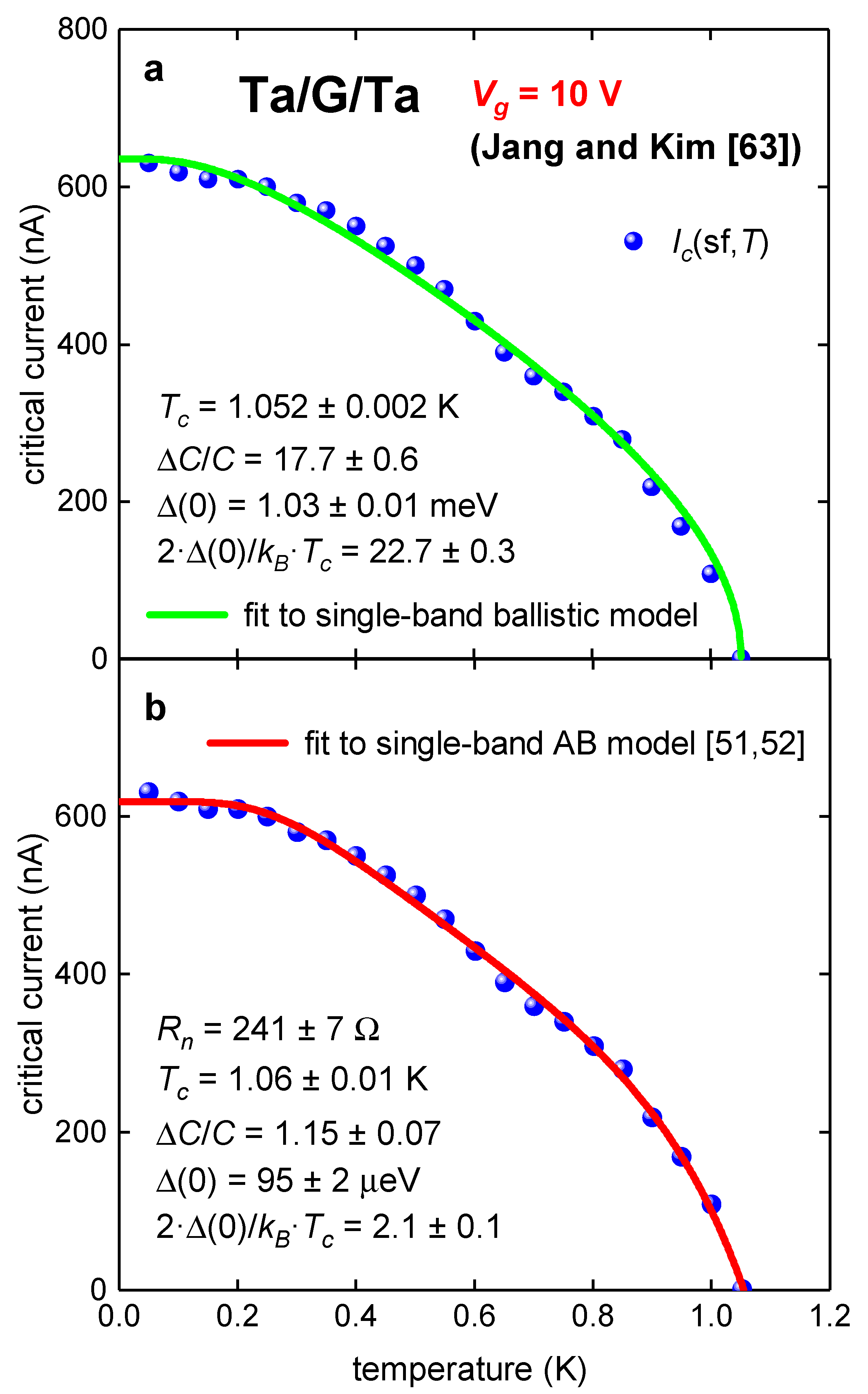
Jang and Kim [63] reported experimental Ic(sf,T) datasets and fit to KO-1 model (in their Figure 2d [63]) for micrometer long ballistic Ta/G/Ta junctions. The Ic(sf,T) fit to KO-1 model (Figure 2d [63]) and deduced parameters are in disagreement with experimental values based on IcRn product. In Figure 1, we show Ic(sf,T) datasets for Device 1 [63] (recorded at gate voltage Vg = 10 V) and fits to single-band ballistic model, Equation (7) (in Figure 1a) and single-band modified AB model Equation (4) (Figure 1b). Device 1 has W = 6 µm, L = 1 µm, and ξs = 16 µm [63]. This means that the ballistic limit of L << ξs is satisfied for these junctions.
Results of fits to both models are presented in Table 1.
Deduced parameters from the fit to ballistic model (Equation (7)) in Figure 1a are in remarkable disagreement with any physical-backgrounded expectations, i.e., the ratio of (which should be comparable with s-wave BCS weak coupling limit of ) and (which should be comparable with s-wave BCS weak coupling limit of ).
It needs to be noted that the highest experimental value for phonon-mediated superconductors of was measured for lead- and bismuth-based alloys [64,65], and the deduced value by the ballistic model does not have a physical interpretation.
In contract, the fit to Equation (4) reveals superconducting parameters in expected ranges of and , i.e., these parameters are slightly suppressed from s-wave BCS weak-coupling limits as expected [52,60]. It should also be noted that free-fitting parameter Rn = 241 ± 7 Ω is in a good agreement with experimental measured value for this junction [63].
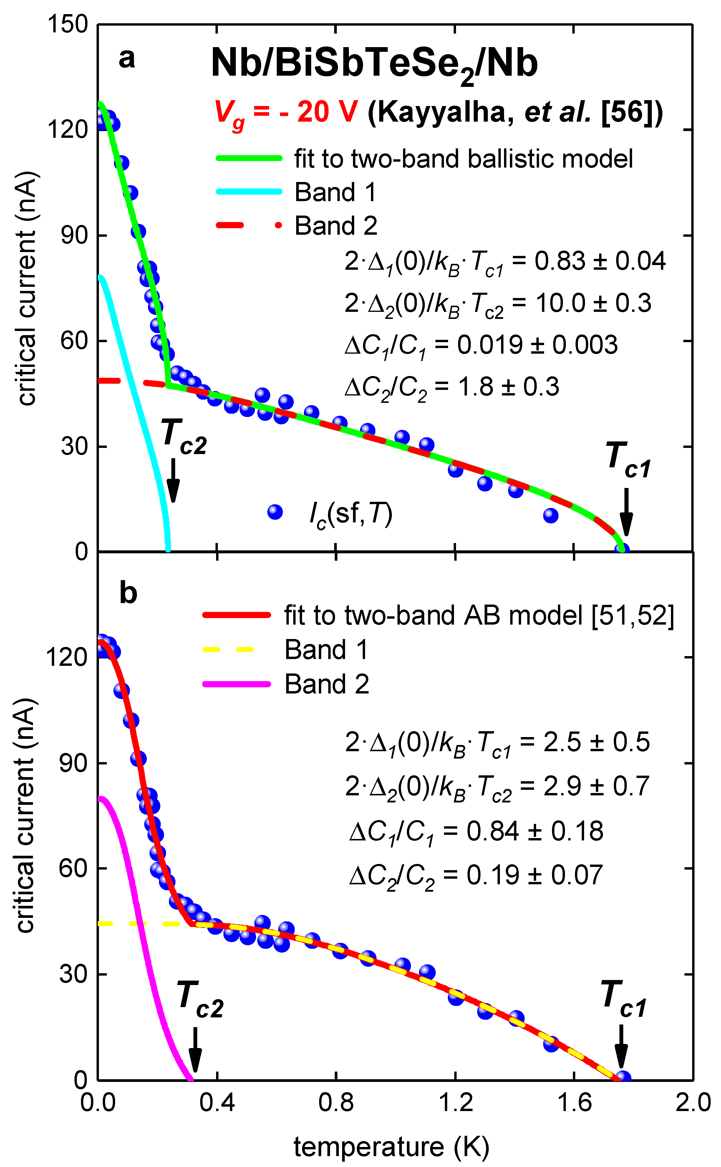
It can be seen (Figure 1), that there is an upturn in experimental Ic(sf,T) at T ~ 0.65 K, which is a manifestation of the second superconducting band opening in this atomically thin S/N/S junction [51,52]. Thus, the experimental Ic(sf,T) dataset was fitted to two-band models (Equations (8) and (5)). Results of these fits are shown in Figure 2 and deduced parameters are in Table 2.
The fit reveals a large disagreement of parameters deduced by ballistic model with expected values within frames for BCS theory. In contrast with this, deduced parameters by modified AB model [51,52] are within weak-coupling limits of BCS. As shown in Reference [51], raw experimental Ic(sf,T) datasets should be reasonably dense to deduce parameters by AB model with small uncertainties.
3.2. Planar Nb/BiSbTeSe2-Nanoribbon/Nb Junctions
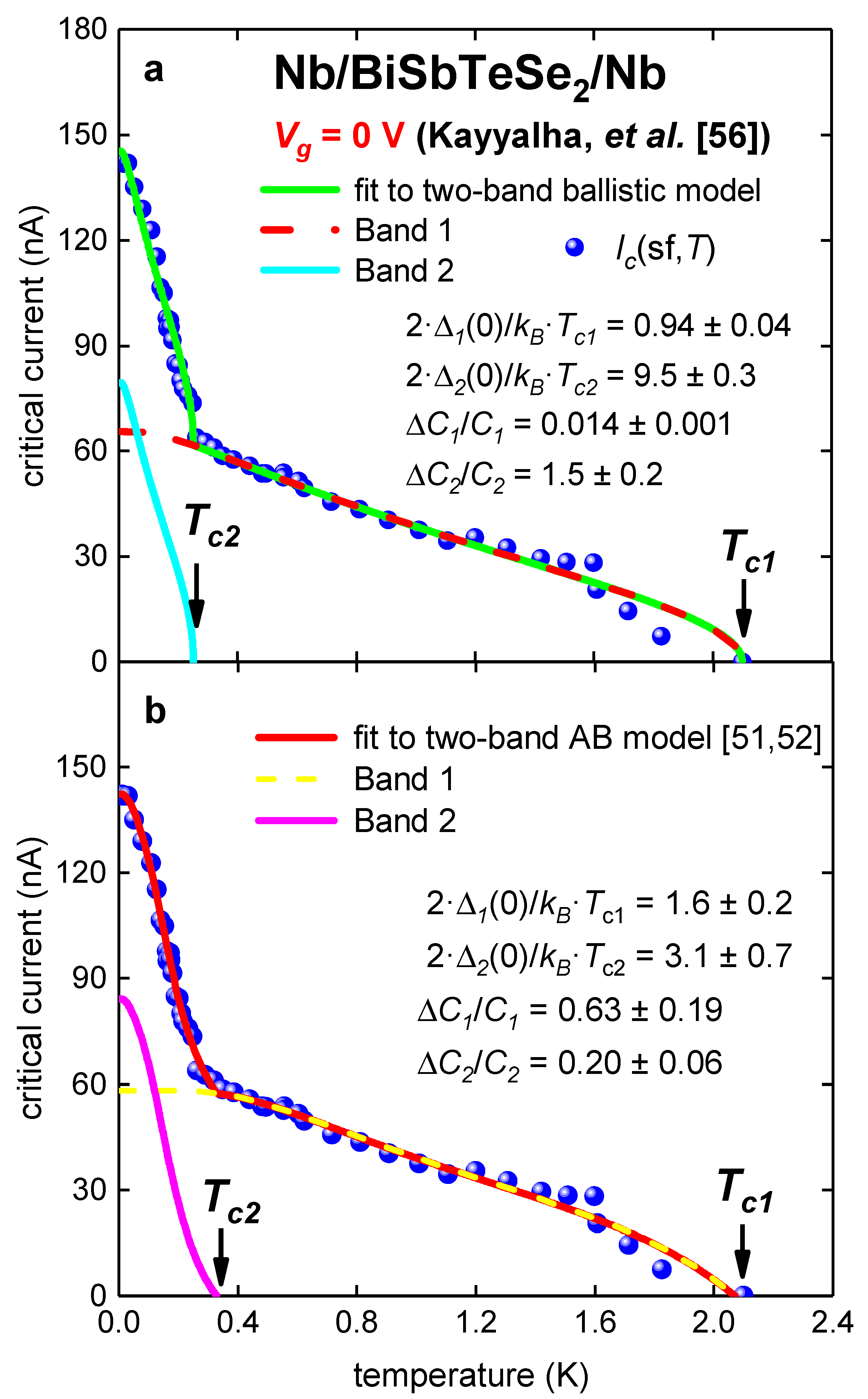
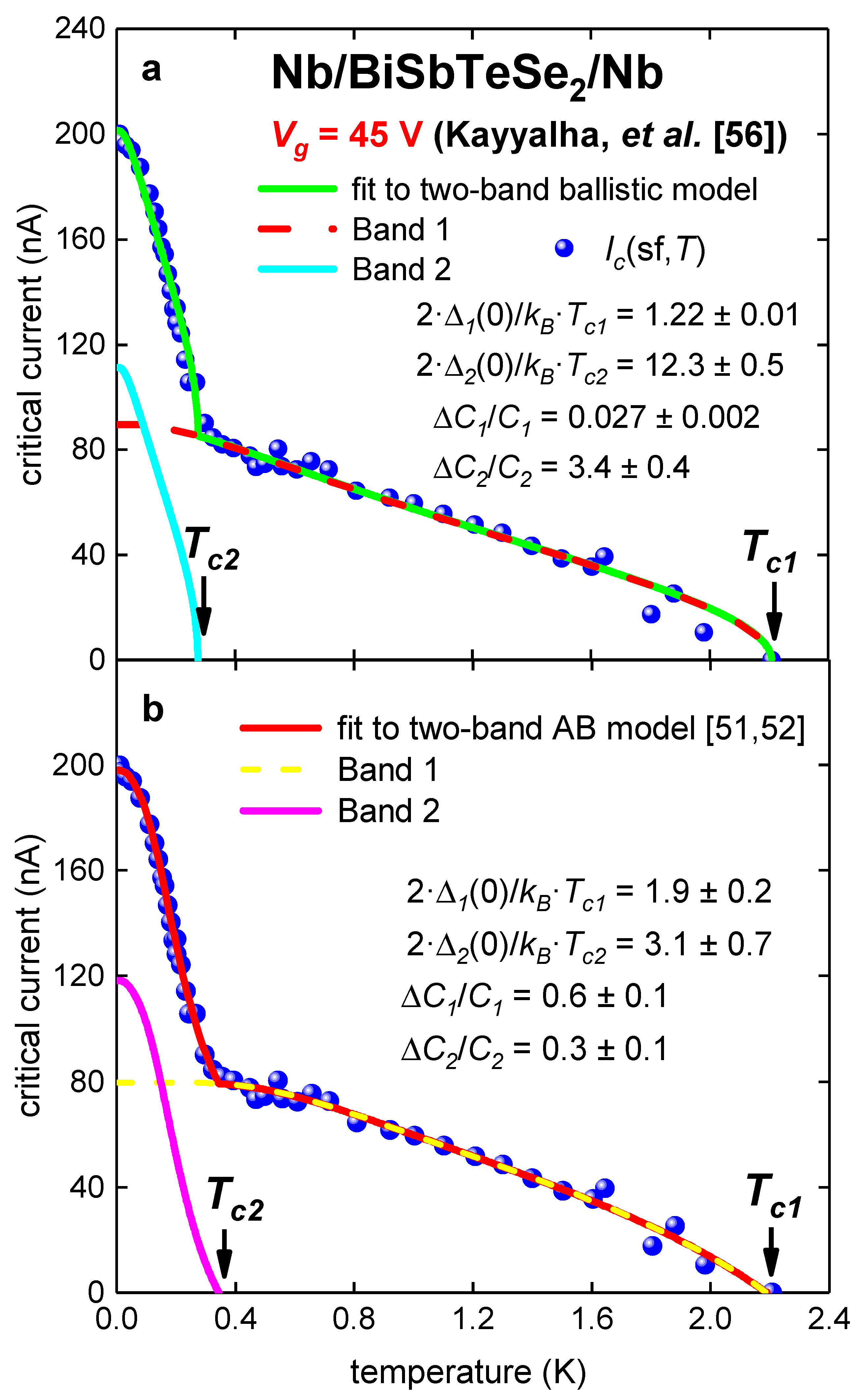
Kayyalha et al. [56] reported Ic(sf,T) for five Nb/BiSbTeSe2-nanopribbon/Nb junctions at different gate voltage, Vg. In this paper Ic(sf,T) datasets for Sample 1 at Vg = −20 V, 0 V and 45 V [56] were analyzed by two-band models (Equations (5) and (8)), because it was already shown in Reference [60] that these junctions exhibit two-band superconducting state. In Figure 3 experimental Ic(sf,T) dataset [56] and fits are shown. For this junction, L = 40 nm [56] and ξs = 640 nm [56]; thus, the ballistic regime, L << ξs, is well satisfied.
Despite the fact that fits to both models have a similar quality, deduced parameters of the superconducting state (Table 3), i.e., ΔCi/Ci, Δi(0), and , for the case of the ballistic models (Figure 3a), similar to the case of Ta/G/Ta junction (Figure 1 and Figure 2), are remarkably different from values expected from BCS theory. Additionally, there are two orders of magnitude difference between deduced ΔCi/Ci for two bands for the same sample, and one order of magnitude for , which is unavoidable evidence that the ballistic model needs to be reexamined. In contrast with this, the fit to the modified AB model [51] (Figure 3b) reveals deduced parameters, including Rni values, in the expected ranges. It should be noted that full analysis (within the modified AB model [52]) of Ic(sf,T) datasets in junctions reported by Kayyalha et al. [56] can be found elsewhere [60].
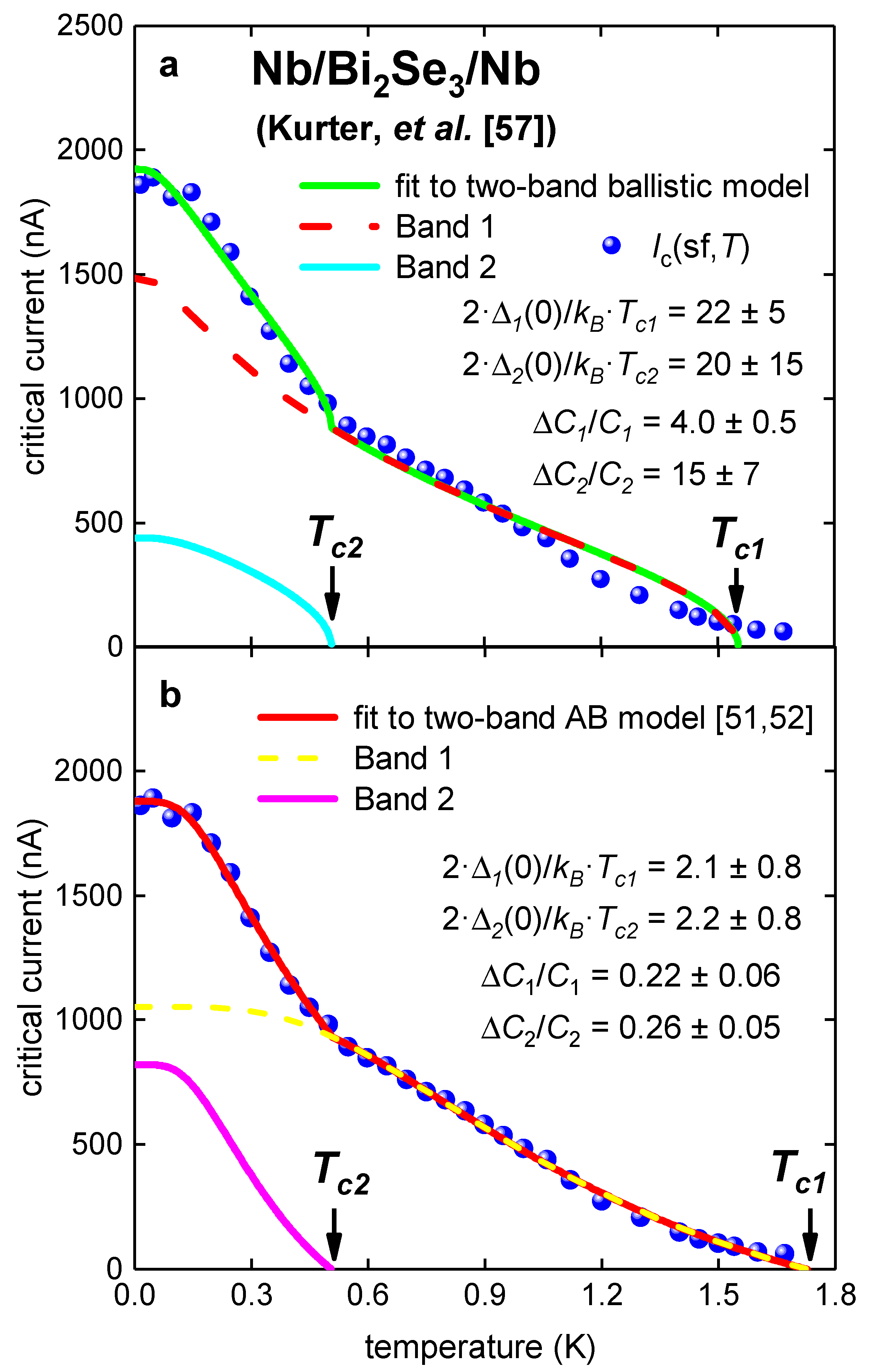
3.3. Planar Nb/Bi2Se3/Nb Junction [56]
In Figure 6, temperature-dependent self-field critical currents, Ic(sf,T), in Nb/Bi2Se3/Nb (W = 1000 nm, L = 100 nm) reported by Kurter et al. [57] is shown. For this junction, 300 nm < ξs < 1,000 nm [57], and thus, the ballistic regime condition, L << ξs, is well satisfied.
4. Discussion
One of the most important questions that can be discussed herein is as follows: what is the origin for such dramatic incapability of ballistic model to analyze the self-field critical currents in S/DCM/S junctions? From the author’s point of view, the origin is the primary concept of the KO theory, in that Ic(sf,T) in the S/N/S junctions is:
where φ is the phase difference between two superconducting electrodes of the junction. Despite this assumption is a fundamental conceptual point of the KO theory, there are no physically background or experimental confirmations that this assumption should be a true. In fact, the analysis of experimental data by a model within this assumption (we presented herein) shows that Equation (9) is in remarkably large disagreement with experiment.
One of the simplest ways to show that Equation (9) is incorrect is to note that when the length of the junction, L, goes to zero, Equation (6) shows:
Herein, the simplest available function [53] that was proposed for the S/DCM/S junction in the Equation (9) was chosen as an example. However, other proposed functions for Equation (9) (for which we refer the reader to Reference [12]) have identical unresolved problem, because, as this was shown for about 100 weak-link superconductors [2,3,4,5,66], the limit should be (Equation (1)):
This means that the primary dissipation mechanism, which governs DC transport current limit in S/N/S, is not yet revealed. However, as we show herein, it is irrelevant to achieving values within the primary concept of KO theory, Equation (9). It should be mentioned that the Density Functional Theory (DFT) calculations [67,68] are currently unexplored powerful techniques, which can be used to reveal dissipation mechanism in S/DCM/S junctions.
5. Conclusions
In this paper, Ic(sf,T) data for S/DCM/S junctions were analyzed by applying two models: the ballistic and the modified Ambegaokar-Baratoff model. It was shown that the ballistic model [10,11,12,53] cannot describe the self-field critical currents in S/DCM/S junctions. In conclusion, the ballistic model should be reexamined in terms of its applicability to describe dissipation-free self-field transport current in S/DCM/S junctions.
Funding
This research was funded by the State Assignment of Minobrnauki of Russia, theme “Pressure” No. AAAA-A18-118020190104-3, and by Act 211 Government of the Russian Federation, contract No. 02.A03.21.0006.
Conflicts of Interest
The funders had no role in the design of the study, in the collection, analyses, or interpretation of data, as well as in the writing of the manuscript, or in the decision to publish the results.
References
- Hirsch, J.E.; Maple, M.B.; Marsiglio, F. Superconducting materials classes: Introduction and overview. Physica C 2015, 514, 1–8. [Google Scholar] [CrossRef] [Green Version]
- Talantsev, E.F.; Tallon, J.L. Universal self-field critical currents for thin-film superconductors. Nat. Commun. 2015, 6, 7820. [Google Scholar] [CrossRef] [PubMed]
- Talantsev, E.F.; Crump, W.P.; Tallon, J.L. Thermodynamic parameters of single-or multi-band superconductors derived from self-field critical currents. Ann. Phys. 2017, 529, 1700197. [Google Scholar] [CrossRef]
- Talantsev, E.F.; Crump, W.P. Weak-link criterion for pnictide and cuprate superconductors. Supercond. Sci. Technol. 2018, 31, 124001. [Google Scholar] [CrossRef]
- Talantsev, E.F.; Crump, W.P.; Tallon, J.L. Universal scaling of the self-field critical current in superconductors: From sub-nanometre to millimetre size. Sci. Rep. 2018, 7, 10010. [Google Scholar] [CrossRef] [PubMed]
- Holm, R.; Meissner, W. Messungen mit Hilfe von flüssigem Helium. XIII. Kontaktwiderstand zwischen Supraleitern und Nichtsupraleitern (Measurements using liquid helium. XIII. Contact resistance between superconductors and non-superconductors). Zeitschrift für Physik 1932, 74, 715–735. [Google Scholar] [CrossRef]
- Ambegaokar, V.; Baratoff, A. Tunneling between superconductors. Phys. Rev. Lett. 1963, 10, 486–489. [Google Scholar] [CrossRef]
- Ambegaokar, V.; Baratoff, A. Errata: Tunneling between superconductors. Phys. Rev. Lett. 1963, 11, 104. [Google Scholar] [CrossRef]
- Josephson, B.D. Possible new effects in superconductive tunneling. Phys. Lett. 1962, 1, 251–253. [Google Scholar] [CrossRef]
- Kulik, I.O.; Omel’yanchuk, A.N. Contribution to the microscopic theory of the Josephson effect in superconducting bridges. JETP Lett. 1975, 21, 96–97. [Google Scholar]
- Kulik, I.O.; Omel’yanchuk, A.N. Properties of superconducting microbridges in the pure limit. Sov. J. Low Temp. Phys. 1977, 3, 459–462. [Google Scholar]
- Kulik, I.; Omelyanchouk, A. The Josephson effect in superconducting constructions: Microscopic theory. J. Phys. Colloq. 1978, 39. [Google Scholar] [CrossRef]
- Lee, G.H.; Lee, H.J. Proximity coupling in superconductor-graphene heterostructures. Rep. Prog. Phys. 2018, 81, 056502. [Google Scholar] [CrossRef] [PubMed] [Green Version]
- Park, J.; Lee, J.H.; Lee, G.-H.; Takane, Y.; Imura, K.-I.; Taniguchi, T.; Watanabe, K.; Lee, H.-J. Short ballistic Josephson coupling in planar graphene junctions with inhomogeneous carrier doping. Phys. Rev. Lett. 2018, 120, 077701. [Google Scholar] [CrossRef]
- Takane, Y.; Imura, K.-I. Quasiclassical theory of the Josephson effect in ballistic graphene junctions. J. Phys. Soc. Jpn. 2012, 81, 094707. [Google Scholar] [CrossRef]
- Strickland, N.M.; Long, N.J.; Talantsev, E.F.; Hoefakker, P.; Xia, J.A.; Rupich, M.W.; Zhang, W.; Li, X.; Kodenkandath, T.; Huang, Y. Nanoparticle additions for enhanced flux pinning in YBCO HTS films. Curr. Appl. Phys. 2008, 8, 372–375. [Google Scholar] [CrossRef]
- Talantsev, E.F.; Strickland, N.M.; Hoefakker, P.; Xia, J.A.; Long, N.J. Critical current anisotropy for second generation HTS wires. Curr. Appl. Phys. 2008, 8, 388–390. [Google Scholar] [CrossRef]
- Chepikov, V.; Mineev, N.; Degtyarenko, P.; Lee, S.; Petrykin, V.; Ovcharov, A.; Vasiliev, A.; Kaul, A.; Amelichev, V.; Kamenev, A.; et al. Introduction of BaSnO3 and BaZrO3 artificial pinning centres into 2G HTS wires based on PLD-GdBCO films. Phase I of the industrial R&D programme at SuperOx. Supercond. Sci. Technol. 2017, 30, 124001. [Google Scholar]
- Paturi, P.; Malmivirta, M.; Hynninen, T.; Huhtinen, H. Angle dependent molecular dynamics simulation of flux pinning in YBCO superconductors with artificial pinning sites. J. Phys. Condens. Matter 2018, 30, 315902. [Google Scholar] [CrossRef]
- Hänisch, J.; Iida, K.; Hühne, R.; Tarantini, C. Fe-based superconducting thin films—Preparation and tuning of superconducting properties. Supercond. Sci. Technol. 2019, 32, 093001. [Google Scholar] [CrossRef]
- Qu, D.-X.; Teslich, N.E.; Dai, Z.; Chapline, G.F.; Schenkel, T.; Durham, S.R.; Dubois, J. Onset of a two-dimensional superconducting phase in a topological-insulator—Normal-metal Bi1−xSbx/Pt junction fabricated by ion-beam techniques. Phys. Rev. Lett. 2018, 121, 037001. [Google Scholar] [CrossRef] [PubMed]
- Li, C.-Z.; Li, C.; Wang, L.-X.; Wang, S.; Liao, Z.-M.; Brinkman, A.; Yu, D.-P. Bulk and surface states carried supercurrent in ballistic Nb-Dirac semimetal Cd3As2 nanowire-Nb junctions. Phys. Rev. B 2018, 97, 115446. [Google Scholar] [CrossRef]
- Reyren, N.; Thiel, S.; Caviglia, A.D.; Kourkoutis, L.F.; Hammerl, G.; Richter, C.; Schneider, C.W.; Kopp, T.; Rüetschi, A.-S.; Jaccard, D.; et al. Superconducting interfaces between insulating oxides. Science 2007, 317, 1196–1199. [Google Scholar] [CrossRef] [PubMed]
- Gozar, A.; Logvenov, G.; Fitting Kourkoutis, L.; Bollinger, A.T.; Giannuzzi, L.A.; Muller, D.A.; Bozovic, I. High-temperature interface superconductivity between metallic and insulating copper oxides. Nature 2008, 455, 782–785. [Google Scholar] [CrossRef] [PubMed]
- Di Castro, D.; Balestrino, G. Superconductivity in interacting interfaces of cuprate-based heterostructures. Supercond. Sci. Technol. 2018, 31, 073001. [Google Scholar]
- Wang, Q.-Y.; Li, Z.; Zhang, W.-H.; Zhang, Z.-C.; Zhang, J.-S.; Li, W.; Ding, H.; OU, Y.-B.; Deng, P.; Chang, K.; et al. Interface-induced high-temperature superconductivity in single unit-cell FeSe films on SrTiO3. Chin. Phys. Lett. 2012, 29, 037402. [Google Scholar] [CrossRef]
- Zhang, W.H.; Sun, Y.; Zhang, J.; Li, F.; Guo, M.; Zhao, Y.; Zhang, H.; Peng, J.; Xing, Y.; Wang, H.; et al. Direct observation of high-temperature superconductivity in one-unit-cell FeSe films. Chin. Phys. Lett. 2014, 31, 017401. [Google Scholar] [CrossRef]
- Ge, J.F.; Liu, Z.L.; Liu, C.; Gao, C.L.; Qian, D.; Xue, Q.K.; Liu, Y.; Jia, J.F. Superconductivity above 100 K in single-layer FeSe films on doped SrTiO3. Nat. Mater. 2015, 14, 285–289. [Google Scholar] [CrossRef]
- Zhang, H.M.; Sun, Y.; Li, W.; Peng, J.P.; Song, C.L.; Xing, Y.; Zhang, Q.; Guan, J.; Li, Z.; Zhao, Y.; et al. Detection of a superconducting phase in a two-atom layer of hexagonal Ga film grown on semiconducting GaN(0001). Phys. Rev. Lett. 2015, 114, 107003. [Google Scholar] [CrossRef]
- Xing, Y.; Zhang, H.M.; Fu, H.L.; Liu, H.; Sun, Y.; Peng, J.P.; Wang, F.; Lin, X.; Ma, X.C.; Xue, Q.K.; et al. Quantum Griffiths singularity of superconductor-metal transition in Ga thin films. Science 2015, 350, 542–545. [Google Scholar] [CrossRef]
- Navarro-Moratalla, E.; Island, J.O.; Mañas-Valero, S.; Pinilla-Cienfuegos, E.; Castellanos-Gomez, A.; Quereda, J.; Rubio-Bollinger, G.; Chirolli, L.; Silva-Guillén, J.A.; Agraït, N.; et al. Enhanced superconductivity in atomically thin TaS2. Nat. Commun. 2016, 7, 11043. [Google Scholar] [CrossRef] [PubMed]
- Yankowitz, M.; Chen, S.; Polshyn, H.; Watanabe, K.; Taniguchi, T.; Graf, D.; Young, A.F.; Dean, C.R. Tuning superconductivity in twisted bilayer graphene. Science 2019, 363, 1059–1064. [Google Scholar] [CrossRef] [PubMed] [Green Version]
- Lucignano, P.; Alfè, D.; Cataudella, V.; Ninno, D.; Cantele, G. The crucial role of atomic corrugation on the flat bands and energy gaps of twisted bilayer graphene at the “magic angle” θ ∼ 1.08°. Phys. Rev. B 2019, 99, 195419. [Google Scholar] [CrossRef]
- Fête, A.; Rossi, L.; Augieri, A.; Senatore, C. Ionic liquid gating of ultra-thin YBa2Cu3O7-x films. Appl. Phys. Lett. 2016, 109, 192601. [Google Scholar] [CrossRef]
- Fête, A.; Senatore, C. Strong improvement of the transport characteristics of YBa2Cu3O7−x grain boundaries using ionic liquid gating. Sci. Rep. 2017, 8, 17703. [Google Scholar] [CrossRef]
- Paradiso, N.; Nguyen, A.-T.; Kloss, K.E.; Strunk, C. Phase slip lines in superconducting few-layer NbSe2 crystals. 2D Mater. 2019, 6, 025039. [Google Scholar] [CrossRef]
- Guo, J.G.; Chen, X.; Jia, X.Y.; Zhang, Q.H.; Liu, N.; Lei, H.C.; Li, S.Y.; Gu, L.; Jin, S.F.; Chen, X.L.; et al. Quasi-two-dimensional superconductivity from dimerization of atomically ordered AuTe2Se4/3 cubes. Nat. Commun. 2017, 8, 871. [Google Scholar] [CrossRef]
- Pan, J.; Guo, C.; Song, C.; Lai, X.; Li, H.; Zhao, W.; Zhang, H.; Mu, G.; Bu, K.; Lin, T.; et al. Enhanced superconductivity in restacked TaS2 nanosheets. J. Am. Chem. Soc. 2017, 139, 4623. [Google Scholar] [CrossRef]
- Ma, Y.; Pan, J.; Guo, C.; Zhang, X.; Wang, L.; Hu, T.; Mu, G.; Huang, F.; Xie, X. Unusual evolution of Bc2 and Tc with inclined fields in restacked TaS2 nanosheets. NPJ Quantum Mater. 2018, 3, 34. [Google Scholar] [CrossRef]
- Desrat, W.; Moret, M.; Briot, O.; Ngo, T.-H.; Piot, B.A.; Jabakhanji, B.; Gil, B. Superconducting Ga/GaSe layers grown by van der Waals epitaxy. Mater. Res. Express 2018, 5, 045901. [Google Scholar] [CrossRef]
- Liu, C.; Lian, C.-S.; Liao, M.-H.; Wang, Y.; Zhong, Y.; Ding, C.; Li, W.; Song, C.-L.; He, K.; Ma, X.-C.; et al. Two-dimensional superconductivity and topological states in PdTe2 thin films. Phys. Rev. Mater. 2018, 2, 094001. [Google Scholar] [CrossRef]
- Peng, J.; Yu, Z.; Wu, J.; Zhou, Y.; Guo, Y.; Li, Z.; Zhao, J.; Wu, C.; Xie, Y. Disorder enhanced superconductivity toward TaS2 monolayer. ACS Nano 2018, 12, 9461–9466. [Google Scholar] [CrossRef] [PubMed]
- De La Barrera, S.C.; Sinko, M.R.; Gopalan, D.P.; Sivadas, N.; Seyler, K.L.; Watanabe, K.; Taniguchi, T.; Tsen, A.W.; Xu, X.; Xiao, D.; et al. Tuning Ising superconductivity with layer and spin-orbit coupling in two-dimensional transition-metal dichalcogenides. Nat. Commun. 2018, 9, 1427. [Google Scholar] [CrossRef] [PubMed]
- Liao, M.; Zang, Y.; Guan, Z.; Li, H.; Gong, Y.; Zhu, K.; Hu, X.-P.; Zhang, D.; Xu, Y.; Wang, Y.-Y.; et al. Superconductivity in few-layer stanene. Nat. Phys. 2018, 14, 344–348. [Google Scholar] [CrossRef]
- Wu, Y.; He, J.; Liu, J.; Xing, H.; Mao, Z.; Liu, Y. Dimensional reduction and ionic gating induced enhancement of superconductivity in atomically thin crystals of 2H-TaSe2. Nanotechnology 2019, 30, 035702. [Google Scholar] [CrossRef]
- Alidoust, M.; Willatzen, M.; Jauho, A.-P. Symmetry of superconducting correlations in displaced bilayers of graphene. Phys. Rev. B 2019, 99, 155413. [Google Scholar] [CrossRef] [Green Version]
- Talantsev, E.F.; Mataira, R.C.; Crump, W.P. Classifying superconductivity in Moiré graphene superlattices. arXiv 2019, arXiv:1902.07410v2. [Google Scholar]
- Rhodes, D.; Yuan, N.F.; Jung, Y.; Antony, A.; Wang, H.; Kim, B.; Chiu, Y.; Taniguchi, T.; Watanabe, K.; Barmak, K.; et al. Enhanced superconductivity in monolayer Td-MoTe2 with tilted Ising spin texture. arXiv 2019, arXiv:1905.06508. [Google Scholar]
- Yang, H.; Gao, Z.-Q.; Wang, F. Effect of defects in superconducting phase of twisted bilayer graphene. arXiv 2019, arXiv:1908.09555v2. [Google Scholar]
- Talantsev, E.F.; Crump, W.P.; Island, J.O.; Xing, Y.; Sun, Y.; Wang, J.; Tallon, J.L. On the origin of critical temperature enhancement in atomically thin superconductors. 2D Mater. 2017, 4, 025072. [Google Scholar] [CrossRef] [Green Version]
- Talantsev, E.F.; Crump, W.P.; Tallon, J.L. Two-band induced superconductivity in single-layer graphene and topological insulator bismuth selenide. Supercond. Sci. Technol. 2018, 31, 015011. [Google Scholar] [CrossRef]
- Talantsev, E.F. Classifying induced superconductivity in atomically thin Dirac-cone materials. Condensed Matter 2019, 4, 83. [Google Scholar] [CrossRef]
- Titov, M.; Beenakker, C.W.J. Josephson effect in ballistic graphene. Phys. Rev. B 2006, 74, 041401. [Google Scholar] [CrossRef] [Green Version]
- Calado, V.E.; Goswami, S.; Nanda, G.; Diez, M.; Akhmerov, A.R.; Watanabe, K.; Taniguchi, T.; Klapwijk, T.M.; Vandersypen, L.M.K. Ballistic Josephson junctions in edge-contacted graphene. Nat. Nanotechnol. 2015, 10, 761–764. [Google Scholar] [CrossRef] [PubMed] [Green Version]
- Borzenets, I.V.; Amet, F.; Ke, C.T.; Draelos, A.W.; Wei, M.T.; Seredinski, A.; Watanabe, K.; Taniguchi, T.; Bomze, Y.; Yamamoto, M.; et al. Ballistic graphene Josephson junctions from the short to the long junction regimes. Phys. Rev. Lett. 2016, 117, 237002. [Google Scholar] [CrossRef]
- Kayyalha, M.; Kargarian, M.; Kazakov, A.; Miotkowski, I.; Galitski, V.M.; Yakovenko, V.M.; Rokhinson, L.P.; Chen, Y.P. Anomalous low-temperature enhancement of supercurrent in topological-insulator nanoribbon Josephson junctions: Evidence for low-energy Andreev bound states. Phys. Rev. Lett. 2019, 122, 047003. [Google Scholar] [CrossRef]
- Kurter, C.; Finck, A.D.K.; Hor, Y.S.; Van Harlingen, D.J. Evidence for an anomalous current–phase relation in topological insulator Josephson junctions. Nat. Commun. 2015, 6, 7130. [Google Scholar] [CrossRef]
- Gross, F.; Chandrasekhar, B.S.; Einzel, D.; Andres, K.; Hirschfeld, P.J.; Ott, H.R.; Beuers, J.; Fisk, Z.; Smith, J.L. Anomalous temperature dependence of the magnetic field penetration depth in superconducting UBe13. Zeitschrift für Physik B Condensed Matter 1986, 64, 175–188. [Google Scholar] [CrossRef]
- Natterer, F.D.; Ha, J.; Baek, H.; Zhang, D.; Cullen, W.G.; Zhitenev, N.B.; Kuk, Y.; Stroscio, J.A. Scanning tunneling spectroscopy of proximity superconductivity in epitaxial multilayer graphene. Phys. Rev. B 2016, 93, 045406. [Google Scholar] [CrossRef] [Green Version]
- Bardeen, J.; Cooper, L.N.; Schrieffer, J.R. Theory of Superconductivity. Phys. Rev. 1957, 108, 1175–1204. [Google Scholar] [CrossRef] [Green Version]
- Dyson, F. A meeting with Enrico Fermi. Nature 2004, 427, 297. [Google Scholar] [CrossRef] [PubMed]
- Piantadosi, S.T. One parameter is always enough. AIP Adv. 2018, 8, 095118. [Google Scholar] [CrossRef]
- Jang, S.; Kim, E. Short ballistic Josephson coupling in micrometer-long tantalum/graphene/tantalum junction. Curr. Appl. Phys. 2019, 19, 436–439. [Google Scholar] [CrossRef]
- Carbotte, J.P. Properties of boson-exchange superconductors. Rev. Mod. Phys. 1990, 62, 1027–1157. [Google Scholar] [CrossRef]
- Nicol, E.J.; Carbotte, J.P. Properties of the superconducting state in a two-band model. Phys. Rev. B 2005, 71, 054501. [Google Scholar] [CrossRef] [Green Version]
- Talantsev, E.F. Evaluation of a practical level of critical current densities in pnictides and recently discovered superconductors. Supercond. Sci. Technol. 2019, 32, 084007. [Google Scholar] [CrossRef]
- Mackinnon, I.D.R.; Talbot, P.C.; Alarco, J.A. Phonon dispersion anomalies and superconductivity in metal substituted MgB2. Comput. Mater. Sci. 2017, 130, 191–203. [Google Scholar] [CrossRef]
- Alarco, J.A.; Talbot, P.C.; Mackinnon, I.D.R. Identification of superconductivity mechanisms and prediction of new materials using Density Functional Theory (DFT) calculations. J. Phys. Conf. Ser. 2018, 1143, 012028. [Google Scholar] [CrossRef]
Figure 1.
Experimental Ic(sf,T) for tantalum/graphene/tantalum (Ta/G/Ta) junction (Device 1) at gate voltage of Vg = 10 V [63] and data fits to single-band ballistic model (Equation (7), Panel a) and single-band modified AB model (Equation (4), Panel b) (a) Ballistic model. fit quality is R = 0.9948; (b) modified AB model [51,52] fit quality is R = 0.9980.

Figure 2.
Experimental Ic(sf,T) for Ta/G/Ta junction (Device 1) at gate voltage of Vg = 10 V [63] and data fits to two-band ballistic model (Equation (8), Panel a) and two-band modified AB model (Equation (5), Panel b). (a) Ballistic model, fit quality is R = 0.9978; (b) modified AB model [51,52]. Derived parameters: Rn1 = 429 ± 184 Ω, Rn2 = 603 ± 209 Ω, fit quality is R = 0.9994.

Figure 3.
Experimental Ic(sf,T) for Nb/BiSbTeSe2-nanoribbon/Nb junction (Sample 1 [56]) at gate voltage Vg = −20 V. (a) Ballistic model, fit quality is R = 0.990; (b) modified AB model [51,52]. Derived parameters: Rn1 = 6.7 ± 1.6 kΩ, Rn2 = 0.75 ± 0.18 kΩ, fit quality is R = 0.9953.

Figure 4.
Experimental Ic(sf,T) for Nb/BiSbTeSe2-nanoribbon/Nb junction (Sample 1 [56]) at gate voltage Vg = 0 V. (a) Ballistic model, fit quality is R = 0.992; (b) modified AB model [51,52]. Derived parameters: Rn1 = 3.9 ± 0.4 kΩ, Rn2 = 0.81 ± 0.15 kΩ, fit quality is R = 0.9965.

Figure 5.
Experimental Ic(sf,T) for Nb/BiSbTeSe2-nanoribbon/Nb junction (Sample 1 [56]) at gate voltage Vg = 45 V. (a) Ballistic model, fit quality is R = 0.994; (b) modified AB model [51,52]. Derived parameters: Rn1 = 3.5 ± 0.3 kΩ, Rn2 = 630 ± 110 Ω, fit quality is R = 0.998.

Figure 6.
Experimental Ic(sf,T) for Nb/Bi2Se3/Nb junction [57]. (a) Ballistic model, fit quality is R = 0.994; (b) modified AB model [51,52]. Derived parameters: Rn1 = 240 ± 100 Ω, Rn2 = 92 ± 33 Ω. Fit quality is R = 0.9991.


Table 1.
Deduced parameters for tantalum/graphene/tantalum (Ta/G/Ta) junction from fit to single-band Titov and Beenakker (TB) [53] and Ambegaokar and Baratoff (AB) [7,8] models.
| Parameter | TB Model | AB Model |
|---|---|---|
| Tc (K) | 1.052 ± 0.002 | 1.06 ± 0.01 |
| ΔC/C | 17.7 ± 0.6 | 1.15 ± 0.07 |
| Δ(0) (meV) | 1.03 ± 0.01 | 0.095 ± 0.002 |
| 2·Δ(0)/kB·Tc | 22.7 ± 0.3 | 2.1 ± 0.1 |
Table 2.
Deduced parameters for tantalum/graphene/tantalum (Ta/G/Ta) junction at Vg = 10 V from fit to two-band Titov and Beenakker (TB) [53] and Ambegaokar and Baratoff (AB) [7,8] models.
| Parameter | TB Model | AB Model |
|---|---|---|
| Tc1 (K) | 1.052 ± 0.001 | 1.053 ± 0.003 |
| Tc2 (K) | 0.61 ± 0.02 | 0.63 ± 0.03 |
| ΔC1/C1 | 17.1 ± 0.6 | 2.2 ± 0.8 |
| ΔC2/C2 | 2.9 ± 3.8 | 1.1 ± 0.9 |
| 2·Δ1(0)/kB·Tc1 | 21 ± 1 | 3.0 ± 0.9 |
| 2·Δ2(0)/kB·Tc2 | 3 ± 1 | 1.9 ± 0.3 |
Table 3.
Deduced parameters for Nb/BiSbTeSe2-nanoribbon/Nb junction (Sample 1 [56]) at Vg = −20 V from fit to two-band Titov and Beenakker (TB) [53] and Ambegaokar and Baratoff (AB) [7,8] models.
| Parameter | TB Model | AB Model |
|---|---|---|
| Tc1 (K) | 1.76 ± 0.01 | 1.74 ± 0.04 |
| Tc2 (K) | 0.236 ± 0.003 | 0.31 ± 0.02 |
| ΔC1/C1 | 0.019 ± 0.03 | 0.84 ± 0.18 |
| ΔC2/C2 | 1.8 ± 0.3 | 0.19 ± 0.07 |
| 2·Δ1(0)/kB·Tc1 | 0.83 ± 0.04 | 2.5 ± 0.5 |
| 2·Δ2(0)/kB·Tc2 | 10.0 ± 0.3 | 2.85 ± 0.70 |
Table 4.
Deduced parameters for for Nb/BiSbTeSe2-nanoribbon/Nb junction (Sample 1 [56]) at Vg = 0 V from fit to two-band Titov and Beenakker (TB) [53] and Ambegaokar and Baratoff (AB) [7,8] models.
| Parameter | TB Model | AB Model |
|---|---|---|
| Tc1 (K) | 2.10 ± 0.01 | 2.07 ± 0.03 |
| Tc2 (K) | 0.252 ± 0.005 | 0.33 ± 0.02 |
| ΔC1/C1 | 0.014 ± 0.001 | 0.6 ± 0.2 |
| ΔC2/C2 | 1.5 ± 0.2 | 0.20 ± 0.06 |
| 2·Δ1(0)/kB·Tc1 | 0.94 ± 0.04 | 1.6 ± 0.2 |
| 2·Δ2(0)/kB·Tc2 | 9.5 ± 0.3 | 3.1 ± 0.7 |
Table 5.
Deduced parameters for for Nb/BiSbTeSe2-nanoribbon/Nb junction (Sample 1 [56]) at Vg = 45 V from fit to two-band Titov and Beenakker (TB) [53] and Ambegaokar and Baratoff (AB) [7,8] models.
| Parameter | TB Model | AB Model |
|---|---|---|
| Tc1 (K) | 2.21 ± 0.01 | 2.19 ± 0.03 |
| Tc2 (K) | 0.274 ± 0.006 | 0.34 ± 0.01 |
| ΔC1/C1 | 0.027 ± 0.002 | 0.6 ± 0.1 |
| ΔC2/C2 | 3.4 ± 0.4 | 0.30 ± 0.08 |
| 2·Δ1(0)/kB·Tc1 | 1.22 ± 0.01 | 1.9 ± 0.2 |
| 2·Δ2(0)/kB·Tc2 | 12.3 ± 0.5 | 3.1 ± 0.7 |
Table 6.
Deduced parameters for for Nb/Bi2Se3/Nb junction [57] from fit to two-band Titov and Beenakker (TB) [53] and Ambegaokar and Baratoff (AB) [7,8] models.
| Parameter | TB Model | AB Model |
| Tc1 (K) | 1.55 ± 0.02 | 1.73 ± 0.05 |
| Tc2 (K) | 0.51 ± 0.03 | 0.51 ± 0.03 |
| ΔC1/C1 | 4.0 ± 0.5 | 0.22 ± 0.06 |
| ΔC2/C2 | 15 ± 7 | 0.26 ± 0.05 |
| 2·Δ1(0)/kB·Tc1 | 22 ± 5 | 2.1 ± 0.8 |
| 2·Δ2(0)/kB·Tc2 | 15 ± 7 | 2.2 ± 0.8 |
© 2019 by the author. Licensee MDPI, Basel, Switzerland. This article is an open access article distributed under the terms and conditions of the Creative Commons Attribution (CC BY) license (http://creativecommons.org/licenses/by/4.0/).
Share and Cite
MDPI and ACS Style
Talantsev, E.F. DC Self-Field Critical Current in Superconductor/Dirac-Cone Material/Superconductor Junctions. Nanomaterials 2019, 9, 1554. https://0-doi-org.brum.beds.ac.uk/10.3390/nano9111554
AMA Style
Talantsev EF. DC Self-Field Critical Current in Superconductor/Dirac-Cone Material/Superconductor Junctions. Nanomaterials. 2019; 9(11):1554. https://0-doi-org.brum.beds.ac.uk/10.3390/nano9111554
Chicago/Turabian StyleTalantsev, Evgueni F. 2019. "DC Self-Field Critical Current in Superconductor/Dirac-Cone Material/Superconductor Junctions" Nanomaterials 9, no. 11: 1554. https://0-doi-org.brum.beds.ac.uk/10.3390/nano9111554
Note that from the first issue of 2016, this journal uses article numbers instead of page numbers. See further details here.