
Functional Performance of Silicon with Periodic Surface Structures Induced by Femtosecond Pulsed Laser


1
School of Power and Mechanical Engineering, Wuhan University, Wuhan 430072, China
2
The Institute of Technological Sciences, Wuhan University, Wuhan 430072, China
*
Author to whom correspondence should be addressed.
Coatings 2022, 12(6), 716; https://0-doi-org.brum.beds.ac.uk/10.3390/coatings12060716
Submission received: 1 May 2022
/
Revised: 15 May 2022
/
Accepted: 18 May 2022
/
Published: 24 May 2022
(This article belongs to the Special Issue Laser Surface Treatments and Additive Manufacturing)
Abstract
:A micro/nano surface structure can produce specific properties, such as super hydrophilicity, low reflectance property, etc. A femtosecond laser-induced periodic surface structure is an important manufacturing process for the micro/nano structure. This research investigated the effects of scanning intervals and laser power on the surface morphology, wetting properties, and reflectance properties of LIPSS based on a silicon wafer. The results showed that the laser power had a significant effect on the surface morphology and wettability of silicon. With the increase of laser power, the surface roughness, etching depth and surface hydrophilicity increased. However, the laser power had little effect on the surface reflectance. The scanning interval had a great influence on the wettability and reflectance property of silicon. With the decrease of the scanning interval, the surface hydrophobicity and reflectance of silicon first decrease and then remain basically stable from 10 μm.
1. Introduction
The manufacturing of a silicon wafer with specific functional surface properties has attracted many researchers. For example, ultrahydrophilic and low reflectivity surfaces have great prospects in many technical applications, such as silicon solar cells [1,2], optoelectronic devices [3], lithium-ion batteries [4], and antibacterial surfaces [5]. Due to the ultrashort pulse time of the femtosecond pulsed laser and the nonlinear absorption caused by ultrahigh laser intensity at the focus, the heat input of the laser processing is very low. Thus, deformation of the processing and heat-affected zone are small, which ensure processing precision and cleanliness [6]. A femtosecond laser is able to induce a periodic surface structure with a microscale or nanoscale dimension to generate some useful surface functional properties, such as enhanced wettability [7], increased light absorption [8], and optical properties of manipulation [9,10].
The tailored surface microstructures can be obtained by adjusting the laser beam parameters, which can obtain the tailored optical, mechanical, or chemical properties of the surface. Tsibidis et al. [11] presented a detailed theoretical model to account for the surface modification and the plasmon-generated periodic surface structure observed during semiconductor irradiation with ultrashort laser pulses in subablation conditions. Han et al. [12] modulated the femtosecond laser power distribution to control the surface ablated structures through a copper grid mask. Fraggelakis et al. [13] studied the effects of double-pulse interpulse delay, fluence distribution, and polarization on the microstructural morphology of the irradiated silicon surface and demonstrated that the interaction between the pulse flux and the arrival order of each component of double pulses had a great influence on the LIPSS structure. Varlamova et al. [14] studied the wettability of the LIPSS-structured silicon target and showed that the wettability was determined by the surface roughness induced by the femtosecond laser on a macro level. Nivas et al. [15] confirmed that the orientation and period of the grooves could be customized using complex light beams or laser wavelengths, similar to the behavior of subwavelength low spatial frequency ripples.
Although the mechanism of interaction and formation dynamics remains controversial, the laser polarization, pulse fluence, pulse duration, and repetition rate were generally considered to be key factors in determining ripple formation [16,17,18,19,20,21]. The scanning interval is also an important parameter affecting the preparation efficiency of the large-size functional surface. A large scanning interval could speed up the LIPSSs’ preparation. It has not been studied in depth.
In this paper, periodic surface structures induced by a femtosecond laser on silicon were prepared with different scanning intervals and laser powers. The effects of the laser processing parameters on the surface morphology, wettability, and optical properties of silicon with LIPSSs were theoretically and experimentally analyzed. Silicon with custom wettability or wettability gradient can be produced easily with the appropriate laser parameters. It is also possible to customize reflectance values and reflectance gradients of silicon easily and quickly.
2. Experimental Procedure and Analysis Methods
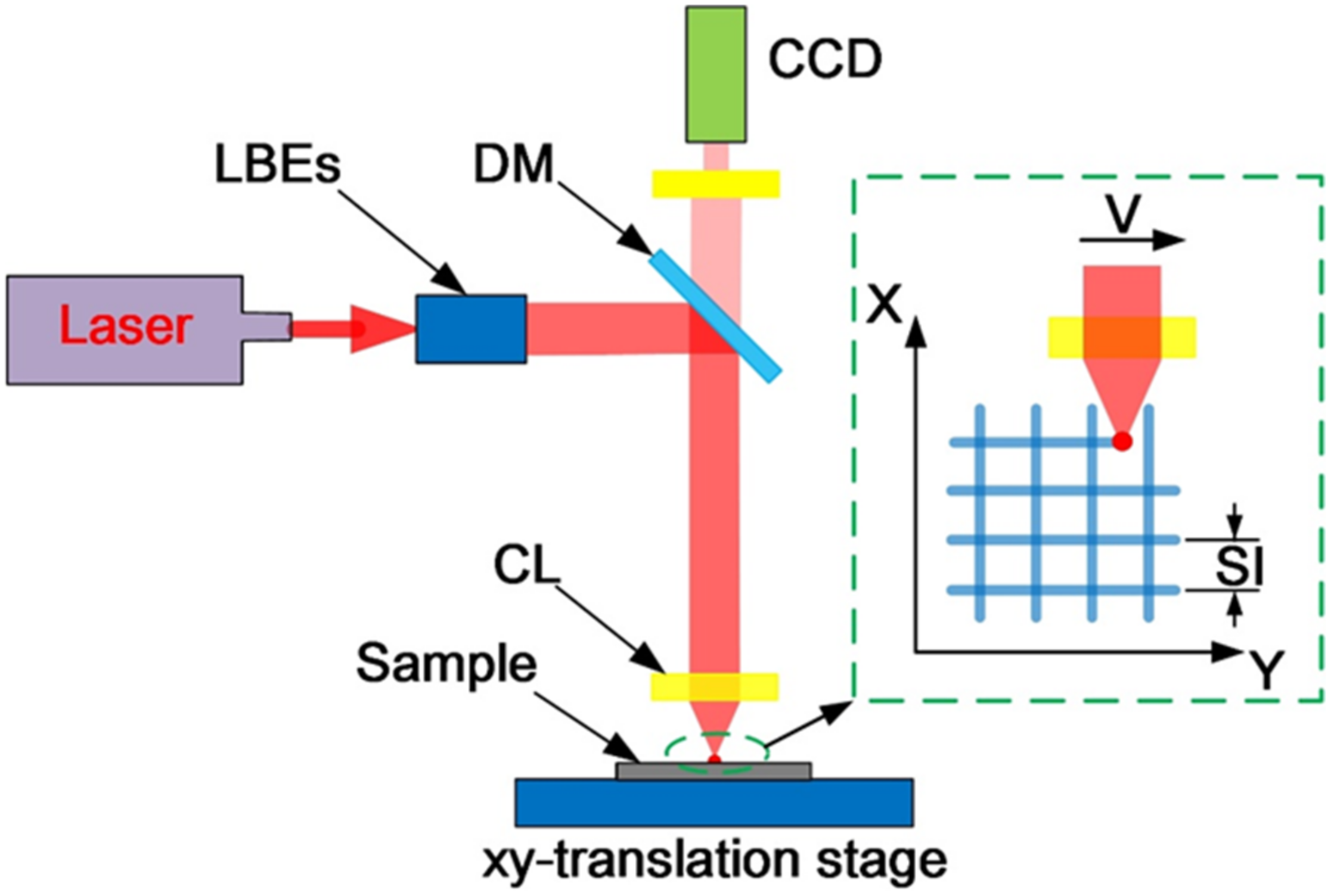
A Coherent Monaco 1035-80-60 femtosecond laser (Coherent, Palo Alto, CA, USA) with a wavelength of 1035 nm and a max single pulse energy of 80 μJ was used in the experiment. The sample of the experiment was a silicon wafer, and the wafer size was 10 mm × 10 mm × 0.50 mm. The silicon wafer was first soaked in deionized water, then washed in an ultrasonic cleaner for 5 min, next soaked in ethanol, then cleaned again in the ultrasonic cleaner for another 5 min, and finally dried to remove surface contaminants. The experimental setup of the LIPSS on silicon is shown in Figure 1. The laser beam focused on the front of the Si target in a vertical incidence manner through the optical path composed of optical lenses. By moving the sample placed on the XY translation table, the laser beam repeatedly scanned the sample at equal intervals in the horizontal and vertical directions to form an equidistant rectangular scanning array on the silicon surface. The main parameters of the femtosecond laser are shown in Table 1.
All experiments were carried out in room temperature air. It is easy to repeat this experiment with the same conditions. After irradiation, the morphology of the LIPSS region was studied by a scanning electron microscope (SEM, Tescan, Brno, Czech Republic) and an optical microscope (OM, Olympus, Tokyo, Japan). The wettability was analyzed by measuring the static contact angle (CA) via the sessile drop method. The value was the average value of the whole immersion area. Finally, the reflection characteristics of sample surface with a wavelength between 200 and 800 nm were measured by UV-VIS spectrophotometer (Shimadzu, Kyoto, Japan), and the reflectance spectrum was obtained.
3. Results and Discussion
3.1. Surface Morphology Analysis
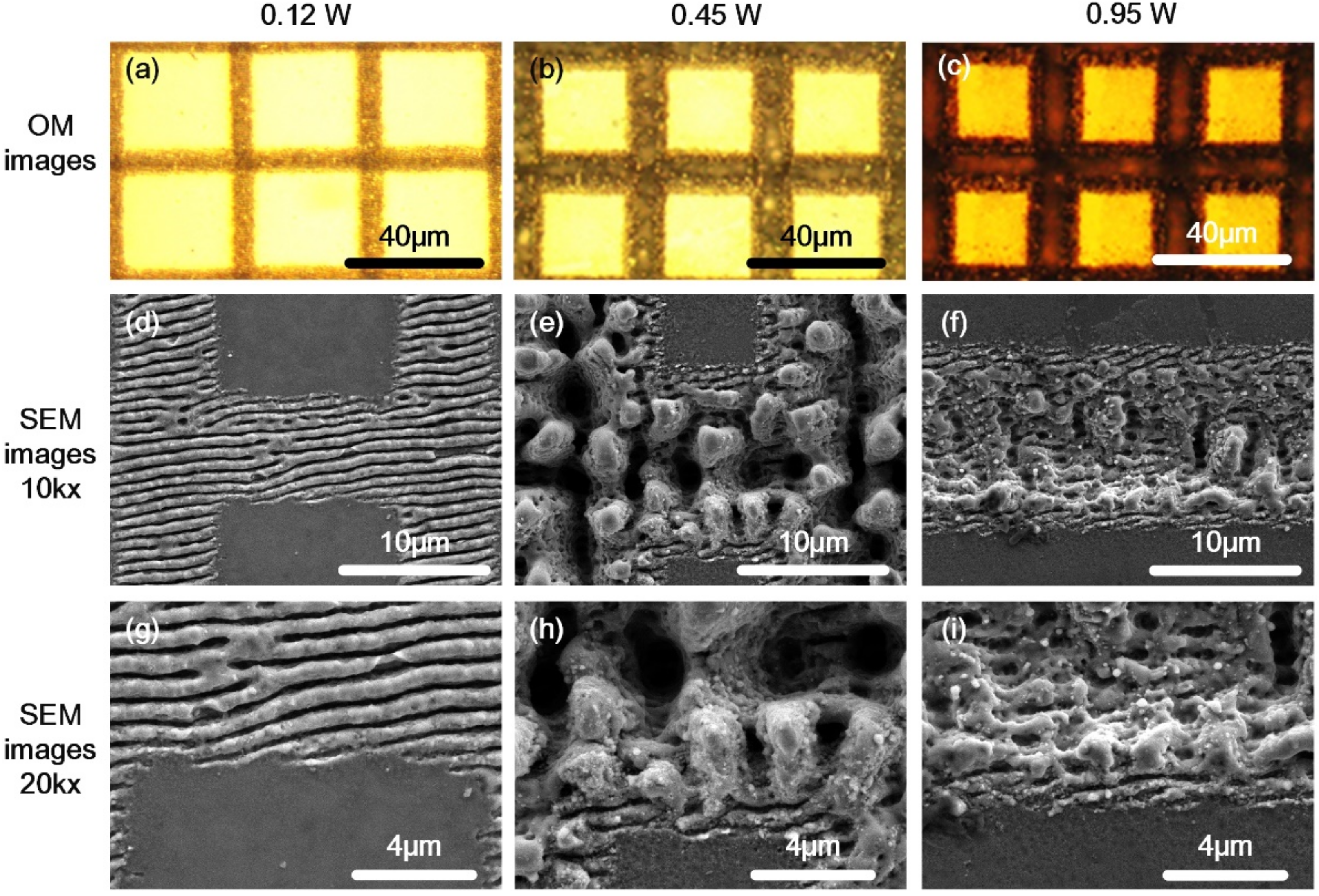
Although the laser irradiation area was the same due to the same scanning interval of 40 μm, the heat-affected zone increased as the laser power increased, as shown in Figure 2. When the laser power was 0.95 W, obvious melting traces and an irregular micron columnar structure appeared on both sides of the laser irradiating area. On the micron columnar structures, there were some small nanoparticles with irregular distribution as shown in Figure 2h. This was because the laser ablation of the material formed some particle groups, some of which were deposited back to the metal surface under the action of gravity and atmospheric pressure due to the loss of initial kinetic energy. These recrystallized structures of melted and sputtered droplets produced in the laser processing were called micro/nano composite structures. When the laser power was 0.45 W, there were only some disordered micron columnar structures, and the size of the structure was larger than that of the structure formed at 0.95 W. When the laser power was 0.12 W, the laser irradiation region was covered by the LIPSS.
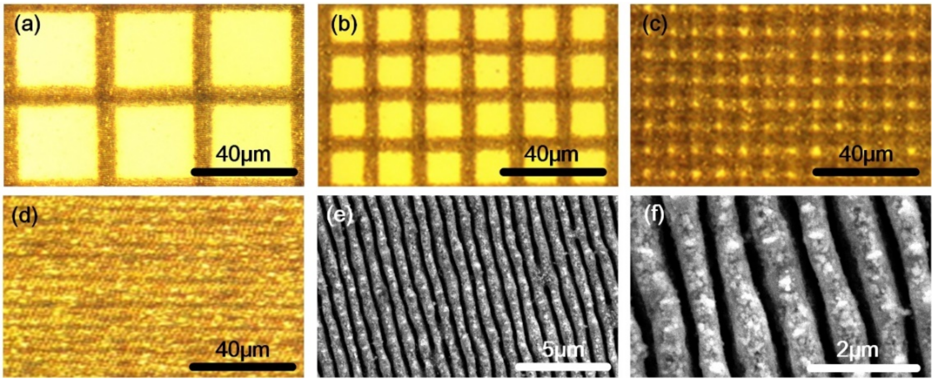
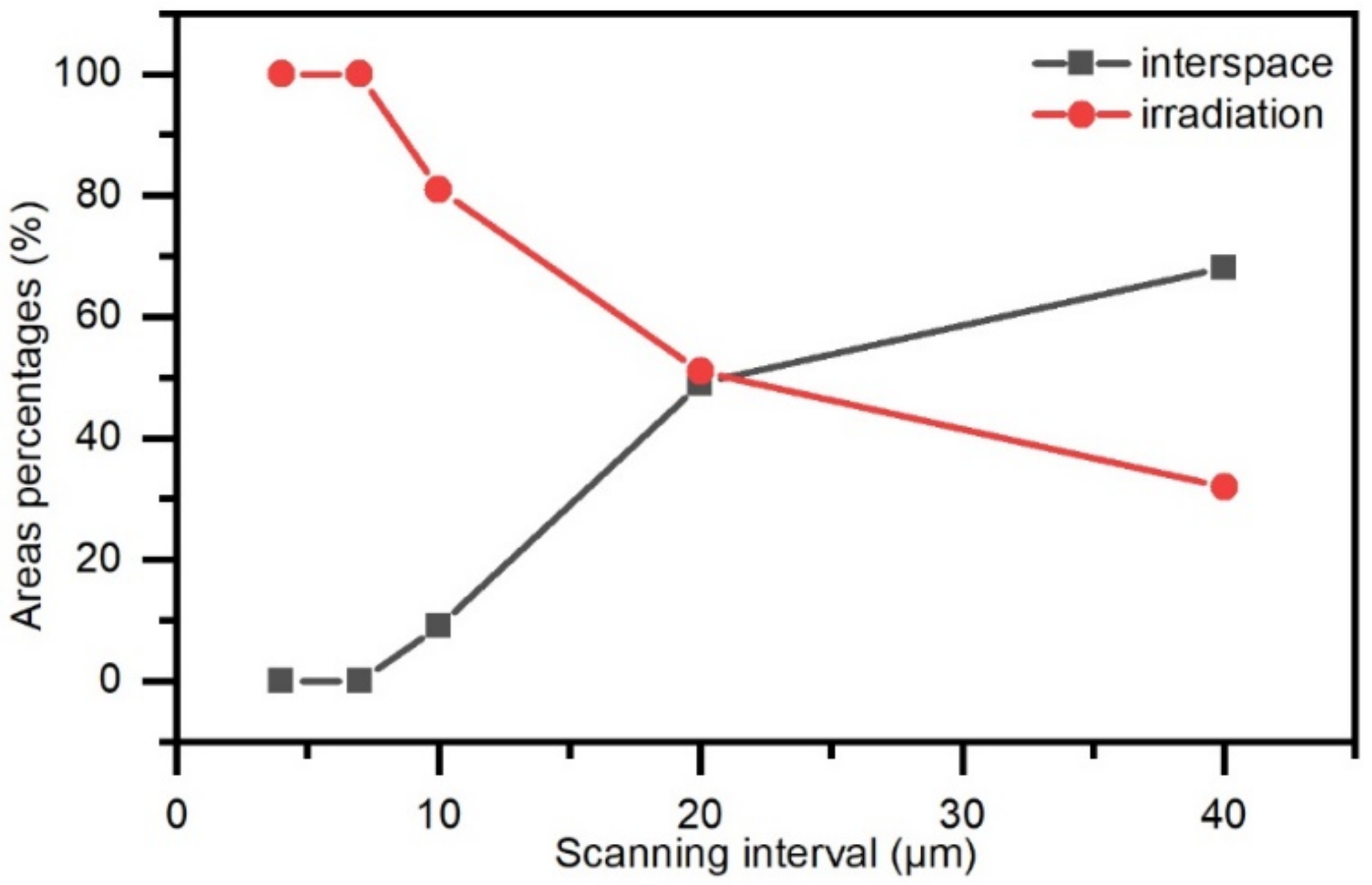
Figure 3 shows the OM and SEM images of silicon irradiated by the femtosecond laser at different scanning intervals. The wider the scanning interval was, the smaller the laser irradiation region area was, as shown in Figure 4. When the scanning interval was 40 μm, the area percentage of the irradiation region was 31.9%. When the scanning interval was 4 μm, the whole silicon surface was irradiated, and regular LIPSSs appeared on the silicon surface, as shown in Figure 3e,f.
3.2. Surface Wettability Analysis
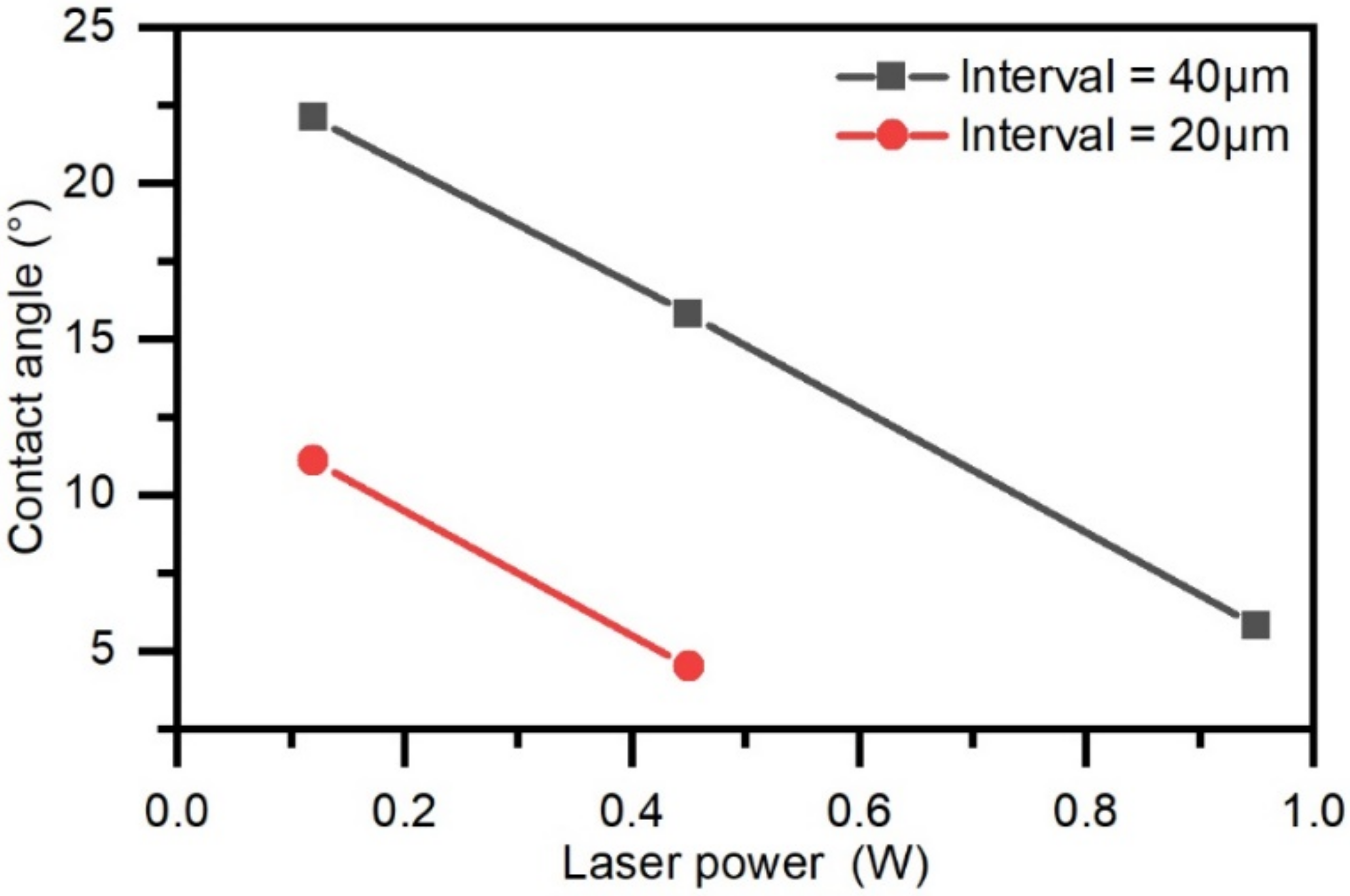
The measurement results of the droplets’ contact angle of silicon irradiated by a femtosecond laser at different laser powers are shown in Figure 5. The contact angle decreased with the increase of laser power. The laser irradiation heat-affected region became wider, and the surface ablation depth became deeper when the laser power increased. Therefore, the wide and deep laser irradiation area directly formed a flow channel, which made the water directly flow into the groove and diffuse on the surface. At the same time, the adhesion between the droplets and the solid surface increased due to the deep depth of the surface ablation.
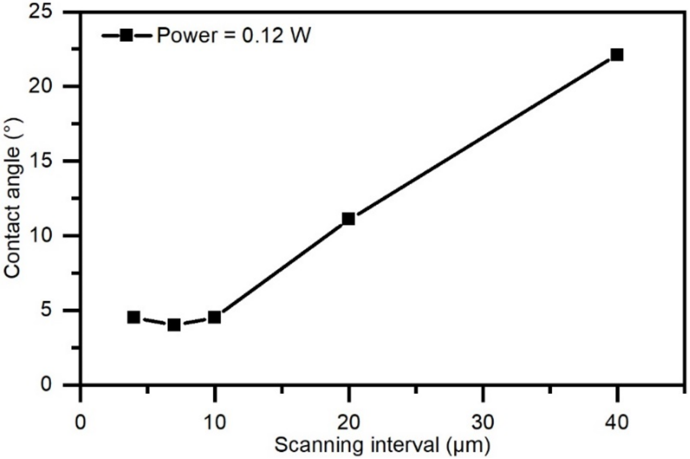
The contact angle decreased with the decreasing scanning interval, as shown in Figure 6. The scanning interval of 40 μm was wider compared with that of 10 μm, so the laser irradiation area was much smaller than the interspace area. Therefore, water droplets dripping on the structure mainly contacted the silicon substrate, which made the contact angle large and close to that of the silicon without a pattern. When the scanning interval decreased, the laser irradiation area increased, so the surface hydrophilicity increased. The contact angle was less than 5° while the scanning interval was less than 10 μm.
3.3. Surface Reflective Performance Analysis
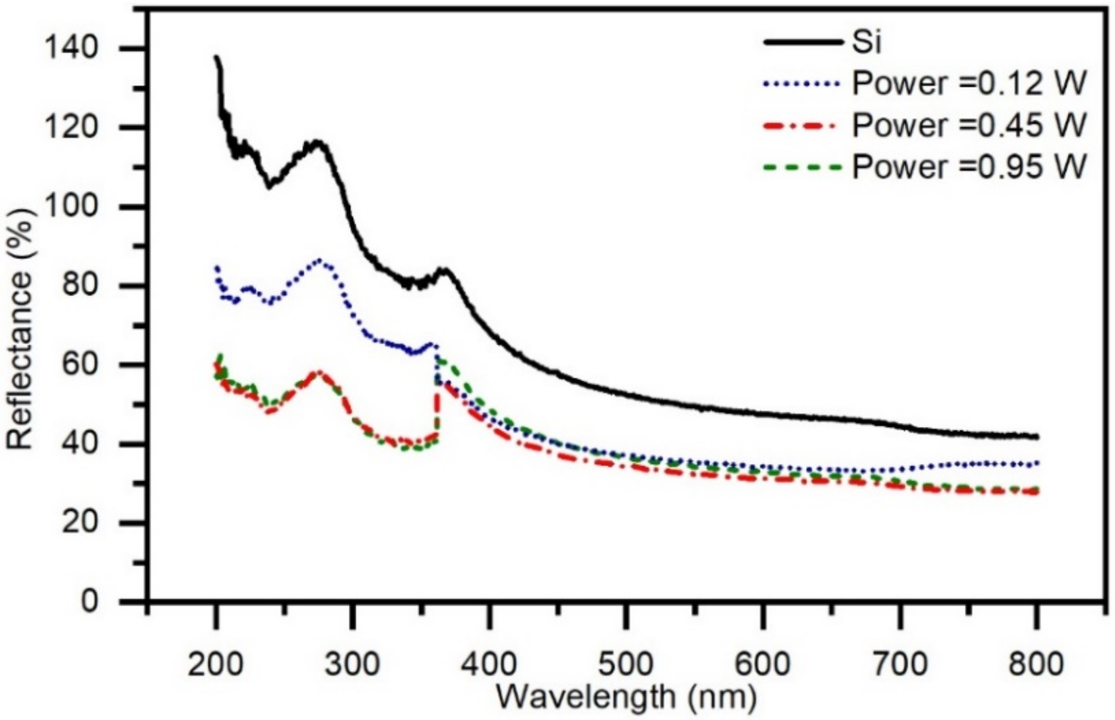
As shown in Figure 7, the reflectivity of silicon, irradiated by a femtosecond laser at a laser power of 0.12 W and scanning interval of 40 μm, decreased with the rising wavelength, but there was a sharp increase in the far and near ultraviolet wavelength range, which was generally consistent with the reflection trend of silicon. Due to the rougher surface morphology and deeper corrosion depth of silicon irradiated by 0.45 W, the reflectivity of silicon irradiated by 0.45 W was less than that by 0.12 W in all wavelengths. However, a high laser power could not further reduce surface reflectivity. The reflection spectrums of silicon irradiated by 0.95 and 0.45 W were roughly the same; the reflectivity decreased about 20%.
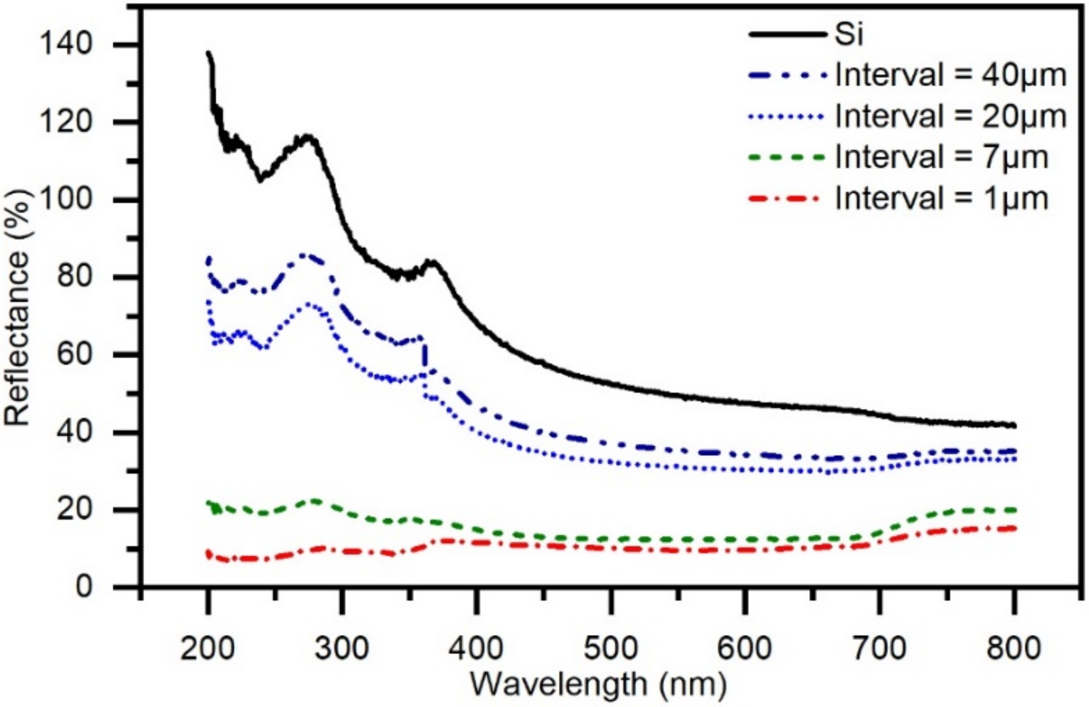
When the scanning interval was 20 μm and the laser power was 0.12 W, the reflectivity was still high and consistent with that of 40 μm, due to the large area of the unirradiated substrate, as shown in Figure 8. When the scanning interval was less than 10 μm, the area of LIPSSs on the silicon wafer, which had good light absorption ability and further reduced the surface reflectivity, was huge. The periodic surface structure formed a resonance region by exciting surface plasmons. It greatly and effectively enhanced the magnetic field intensity near the region, increased the absorption of incident light, and reduced the reflection of light in a wide wavelength range, especially in the visible and infrared regions. In the short wavelength band, because the wavelength of incident light was less than or close to the structural size of the silicon nanowire array, the scattering effect of incident light was dominant, which prolonged the path length of light and increased the absorption of incident light. The overall effect of the absorption mechanism led to a high absorption of all wavelength light on the etched surface, so the silicon surface is black. Compared with colored materials, the angle and polarization of the incident light had little effect on the light absorption performance of silicon.
4. Conclusions and Further Research
The influence of the scanning interval and laser power on the surface morphology, wetting property, and light absorption property of LIPSS based on the silicon wafer were studied. The research found some relationships between the laser parameters and properties.
(1) Laser power had great influence on the wettability of silicon with LIPSS. When the scanning interval was 20 μm and the laser power was higher than 0.45 W, the silicon surface had super hydrophilicity. When the scanning interval was 40 μm and the laser power was higher than 0.95 W, the silicon surface also had super hydrophilicity.
(2) Laser power had little influence on the light absorption property. High laser power could not further change the surface reflectance spectra.
(3) The scanning interval had a significant effect on the wetting properties and light absorption property. When the laser power was 0.12 W and the scanning distance was less than 10 μm, the silicon surface had super hydrophilicity and low light reflectivity, which was called black silicon.
In summary, the scanning interval was a key parameter affecting the wetting and optical properties of silicon with LIPSS. Laser power had a major impact on the wetting property of silicon with LIPSS. Laser parameters can be further studied and optimized to obtain silicon with custom properties, in particular, defining the wetting gradient to achieve a controlled motion of droplets on the silicon surface. The formation mechanism of LIPSS and the influence of laser parameters on other properties are still worth further study.
Author Contributions
Conceptualization, C.Z.; methodology, C.Z.; investigation, Y.C. and X.H.; writing—original draft preparation, Y.C.; writing—review and editing, C.Z.; supervision, C.Z.; project administration, W.P. All authors have read and agreed to the published version of the manuscript.
Funding
This research was funded by the National Key Research and Development Program of China (Grant No. 2018YFB1107701).
Institutional Review Board Statement
Not applicable.
Informed Consent Statement
Not applicable.
Data Availability Statement
The authors confirm that the data supporting the findings of this study are available within the article.
Conflicts of Interest
The authors declare no conflict of interest.
References
- Rahman, T.; Bonilla, R.S.; Nawabjan, A.; Wilshaw, P.R.; Boden, S.A. Passivation of all-angle black surfaces for silicon solar cells. Sol. Energy Mater. Solar Cells 2017, 160, 444–453. [Google Scholar] [CrossRef] [Green Version]
- Chu, D.; Yao, P.; Huang, C. Anti-reflection silicon with self-cleaning processed by femtosecond laser. Opt. Laser Technol. 2021, 136, 106790. [Google Scholar] [CrossRef]
- Leung, S.-F.; Zhang, Q.; Xiu, F.; Yu, D.; Ho, J.C.; Li, D.; Fan, Z. Light management with nanostructures for optoelectronic devices. J. Phys. Chem. Lett. 2014, 5, 1479–1495. [Google Scholar] [CrossRef] [PubMed]
- Vu, A.; Qian, Y.; Stein, A. Porous electrode materials for lithium-ion batteries-how to prepare them and what makes them special. Adv. Energy Mater. 2012, 2, 1056–1085. [Google Scholar] [CrossRef]
- Ivanova, E.P.; Hasan, J.; Webb, H.K.; Gervinskas, G.; Juodkazis, S.; Truong, V.K.; Wu, A.H.; Lamb, R.N.; Baulin, V.A.; Watson, G.S. Bactericidal activity of black silicon. Nat. Commun. 2013, 4, 2838. [Google Scholar] [CrossRef]
- Luong, K.P.; Tanabe-Yamagishi, R.; Yamada, N.; Ito, Y. Micromachining of the back surface and interior of Si using infrared femtosecond laser pulses. J. Laser Appl. 2020, 32, 012017. [Google Scholar] [CrossRef]
- Zorba, V.; Persano, L.; Pisignano, D.; Athanassiou, A.; Stratakis, E.; Cingolani, R.; Tzanetakis, P.; Fotakis, C. Making silicon hydrophobic: Wettability control by two-lengthscale simultaneous patterning with femtosecond laser irradiation. Nanotechnology 2006, 17, 3234. [Google Scholar] [CrossRef]
- Vorobyev, A.; Guo, C. Direct creation of black silicon using femtosecond laser pulses. Appl. Surf. Sci. 2011, 257, 7291–7294. [Google Scholar] [CrossRef]
- Guay, J.-M.; Lesina, A.C.; Baxter, J.; Charron, M.; Côté, G.; Ramunno, L.; Berini, P.; Weck, A. Enhanced plasmonic coloring of silver and formation of large laser-induced periodic surface structures using multi-burst picosecond pulses. arXiv 2016, arXiv:1609.04847. [Google Scholar]
- Dusser, B.; Sagan, Z.; Soder, H.; Faure, N.; Colombier, J.-P.; Jourlin, M.; Audouard, E. Controlled nanostructrures formation by ultra fast laser pulses for color marking. Opt. Express 2010, 18, 2913–2924. [Google Scholar] [CrossRef] [Green Version]
- Tsibidis, G.D.; Barberoglou, M.; Loukakos, P.A.; Stratakis, E.; Fotakis, C. Dynamics of ripple formation on silicon surfaces by ultrashort laser pulses in subablation conditions. Phys. Rev. B 2012, 86, 115316. [Google Scholar] [CrossRef] [Green Version]
- Han, W.; Jiang, L.; Li, X.; Liu, Y.; Lu, Y. Femtosecond laser induced tunable surface transformations on (111) Si aided by square grids diffraction. Appl. Phys. Lett. 2015, 107, 251601. [Google Scholar] [CrossRef] [Green Version]
- Fraggelakis, F.; Stratakis, E.; Loukakos, P. Control of periodic surface structures on silicon by combined temporal and polarization shaping of femtosecond laser pulses. Appl. Surf. Sci. 2018, 444, 154–160. [Google Scholar] [CrossRef]
- Varlamova, O.; Reif, J.; Stolz, M.; Borcia, R.; Borcia, I.D.; Bestehorn, M. Wetting properties of LIPSS structured silicon surfaces. Eur. Phys. J. B 2019, 92, 1–8. [Google Scholar] [CrossRef]
- Nivas, J.J.; Amoruso, S. Generation of supra-wavelength grooves in femtosecond laser surface structuring of silicon. Nanomaterials 2021, 11, 174. [Google Scholar] [CrossRef] [PubMed]
- Han, W.; Jiang, L.; Li, X.; Liu, P.; Xu, L.; Lu, Y. Continuous modulations of femtosecond laser-induced periodic surface structures and scanned line-widths on silicon by polarization changes. Opt. Express 2013, 21, 15505–15513. [Google Scholar] [CrossRef] [Green Version]
- Sartori, A.F.; Orlando, S.; Bellucci, A.; Trucchi, D.M.; Abrahami, S.; Boehme, T.; Hantschel, T.; Vandervorst, W.; Buijnsters, J.G. Laser-induced periodic surface structures (LIPSS) on heavily boron-doped diamond for electrode applications. ACS Appl. Mater. Interfaces 2018, 10, 43236–43251. [Google Scholar] [CrossRef] [Green Version]
- Fraggelakis, F.; Mincuzzi, G.; Lopez, J.; Manek-Hönninger, I.; Kling, R. Texturing metal surface with MHz ultra-short laser pulses. Opt. Express 2017, 25, 18131–18139. [Google Scholar] [CrossRef] [Green Version]
- Zhao, J.; Zhang, C.; Liu, F.; Cheng, G. Understanding femtosecond laser internal scribing of diamond by atomic simulation: Phase transition, structure and property. Carbon 2021, 175, 352–363. [Google Scholar] [CrossRef]
- Liu, R.; Zhang, D.; Ji, S.; Cai, Y.; Liang, C.; Li, Z. Femtosecond Laser Generated Hierarchical Macropore/LIPSS Metasurfaces and Their Ultrabroadband Absorbance, Photothermal Properties, and Thermal-Induced Reflectance Oscillation. ACS Appl. Electron. Mater. 2022, 4, 990–1001. [Google Scholar] [CrossRef]
- Jalil, S.A.; Yang, J.; ElKabbash, M.; Cong, C.; Guo, C. Formation of controllable 1D and 2D periodic surface structures on cobalt by femtosecond double pulse laser irradiation. Appl. Phys. Lett. 2019, 115, 031601. [Google Scholar] [CrossRef]
Figure 1.
Experimental setup. Component abbreviations: LBEs: laser beam extenders; CCD: CCD camera; DM: dichroic mirror; CL: convex lens; SI: scanning interval.
Figure 1.
Experimental setup. Component abbreviations: LBEs: laser beam extenders; CCD: CCD camera; DM: dichroic mirror; CL: convex lens; SI: scanning interval.

Figure 2.
OM and SEM images of Si irradiated by a femtosecond laser at different laser powers. (a–c) OM images of a silicon wafer irradiated by a femtosecond laser at the scanning interval of 40 μm and the laser power of 0.12, 0.45, and 0.95 W, respectively. (d–f) 10kx SEM images of a silicon wafer irradiated by a femtosecond laser at the scanning interval of 40 μm and the laser power of 0.12, 0.45, and 0.95 W, respectively. (g–i) 20kx SEM images of a silicon wafer irradiated by a femtosecond laser at the scanning interval of 40 μm and the laser power of 0.12, 0.45, and 0.95 W, respectively.

Figure 3.
OM and SEM images of Si irradiated by a femtosecond laser at different scanning intervals. (a–d) OM images of a silicon wafer irradiated by a femtosecond laser at the laser power of 0.12 W and the scanning interval of 40, 20, 10, and 4 μm, respectively. (e,f) SEM images of a silicon wafer irradiated by a femtosecond laser at the laser power of 0.12 W and the scanning interval of 4 μm.

Figure 4.
Areas percentages of the laser irradiation region and the interspace region at different scanning intervals.
Figure 4.
Areas percentages of the laser irradiation region and the interspace region at different scanning intervals.

Figure 5.
Contact angle of silicon irradiated by a femtosecond laser at different laser powers.

Figure 6.
Contact angle of silicon irradiated by a femtosecond laser at different scanning intervals.
Figure 6.
Contact angle of silicon irradiated by a femtosecond laser at different scanning intervals.

Figure 7.
Reflectance spectra of silicon irradiated by a femtosecond laser at different laser powers.
Figure 7.
Reflectance spectra of silicon irradiated by a femtosecond laser at different laser powers.

Figure 8.
Reflectance spectra of silicon irradiated by a femtosecond laser at different scanning intervals.
Figure 8.
Reflectance spectra of silicon irradiated by a femtosecond laser at different scanning intervals.


Table 1.
Femtosecond laser processing parameters.
| Parameter | Value |
|---|---|
| wave length (nm) | 1035 |
| pulse duration (fs) | 270 |
| laser frequency (kHz) | 375 |
| scanning speed (mm/s) | 1200 |
| laser power (W) | 0.95, 0.45, 0.12 |
| scanning interval (μm) | 40, 20, 10, 7, 4, 1 |
Publisher’s Note: MDPI stays neutral with regard to jurisdictional claims in published maps and institutional affiliations. |
© 2022 by the authors. Licensee MDPI, Basel, Switzerland. This article is an open access article distributed under the terms and conditions of the Creative Commons Attribution (CC BY) license (https://creativecommons.org/licenses/by/4.0/).
Share and Cite
MDPI and ACS Style
Chen, Y.; Peng, W.; Hu, X.; Zhang, C. Functional Performance of Silicon with Periodic Surface Structures Induced by Femtosecond Pulsed Laser. Coatings 2022, 12, 716. https://0-doi-org.brum.beds.ac.uk/10.3390/coatings12060716
AMA Style
Chen Y, Peng W, Hu X, Zhang C. Functional Performance of Silicon with Periodic Surface Structures Induced by Femtosecond Pulsed Laser. Coatings. 2022; 12(6):716. https://0-doi-org.brum.beds.ac.uk/10.3390/coatings12060716
Chicago/Turabian StyleChen, Yong, Weiping Peng, Xiaofeng Hu, and Chen Zhang. 2022. "Functional Performance of Silicon with Periodic Surface Structures Induced by Femtosecond Pulsed Laser" Coatings 12, no. 6: 716. https://0-doi-org.brum.beds.ac.uk/10.3390/coatings12060716
Note that from the first issue of 2016, this journal uses article numbers instead of page numbers. See further details here.