Sputtering Physical Vapour Deposition (PVD) Coatings: A Critical Review on Process Improvement and Market Trend Demands

 , ,
, ,
Abstract
:1. Introduction
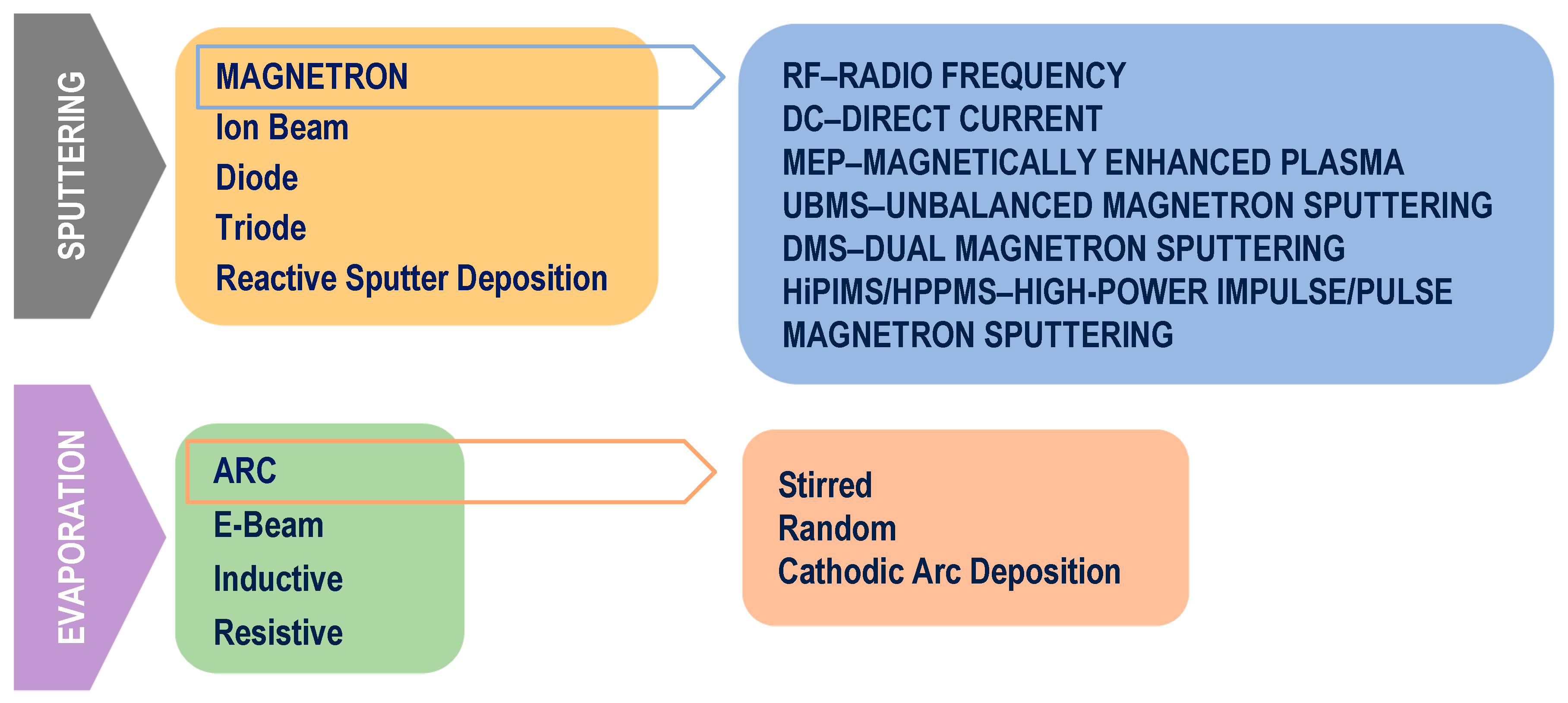
2. PVD Coatings
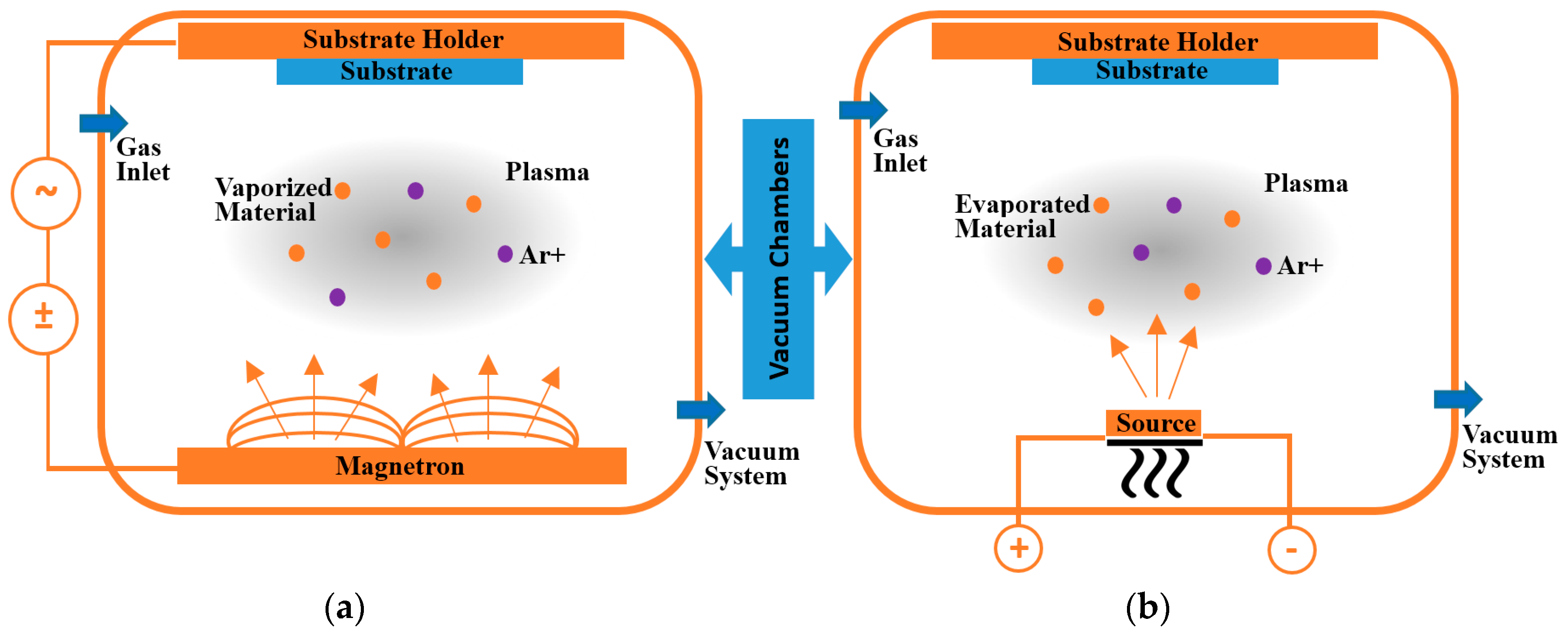
2.1. Evaporation and Sputtering Principles
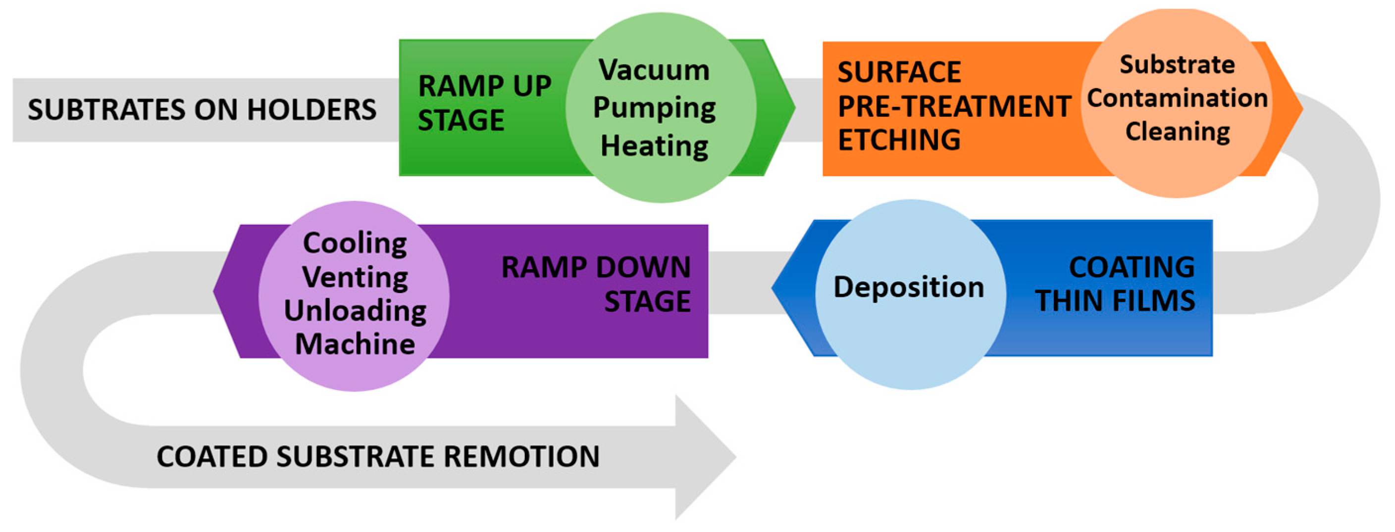
2.2. Sputtering Process Steps
- The first step—Ramp up—involves the preparation of the vacuum chamber, which consists in a gradual increase of the temperature, induced by a tubular heating and a modular control system; at the same time, the vacuum pumps are activated in order to decrease the pressure inside the chamber. In this type of sputtering reactors, two pumps are used, the first one (primary vacuum) produces a pressure up to 10−5 bar, the second one (high vacuum) reaches 10−7 bar pressure.
- The second step—Etching—is characterized by cathodic cleaning. The substrate is bombarded by ions from plasma etching to clean contaminations located on the substrate surface. This is an important preparation step for a deposition because it helps to increase adhesion. Indeed, the substrate properties have a direct influence on adhesion, such as substrate material, hardness and surface quality [62,63].
- In the third step—Coating—takes place. The material to be deposited is projected to the substrate surface. Several materials can be used; among these are titanium, zirconium, and chromium nitrides or oxides, among others.
- The last step—Ramp downstage—corresponds to the vacuum chamber returning to room temperature and ambient pressure. In order to achieve this, a specific cooling system is used—chiller—with two sets of water knockout drums: one is used for the vacuum pumps and the other for cooling targets. Equipment unloading and cooling should not damage coatings’ properties. The need for a cooling system is a drawback because it decreases production rate and rises energetic costs.
2.3. Deposition Process Influence Coatings Properties
3. Sputtering Depositions Improvements
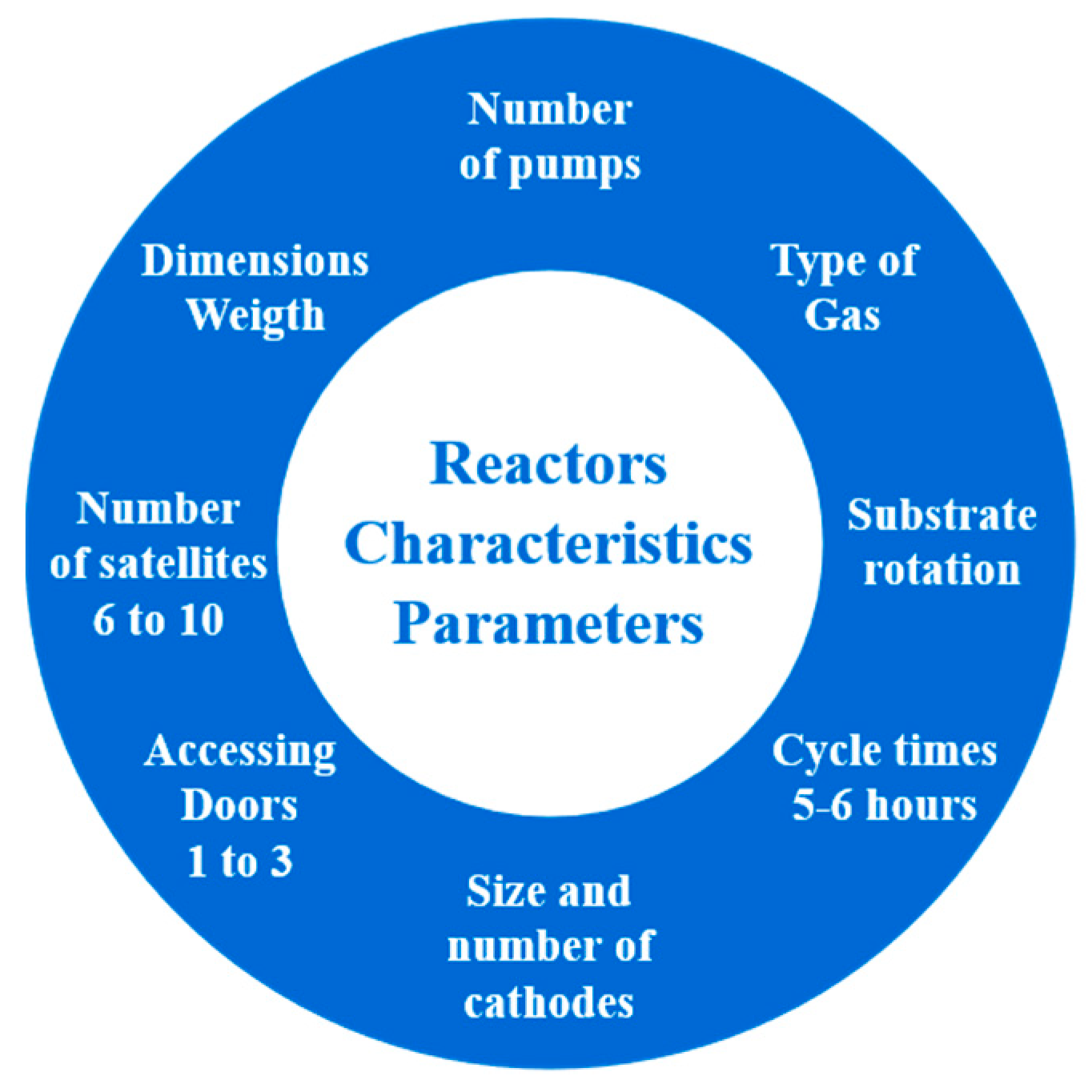
3.1. Reactors’ Parameters and Characteristics
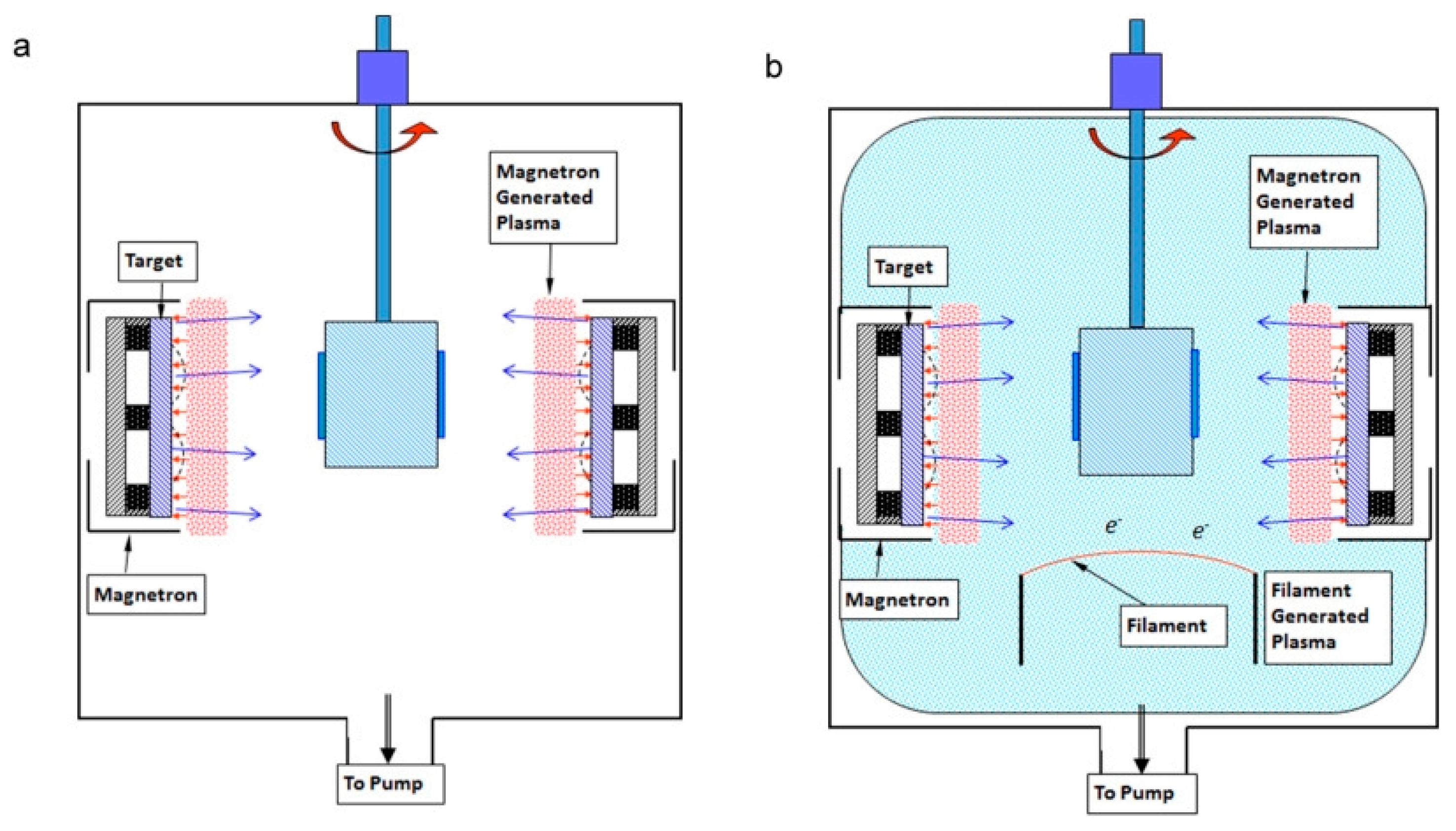
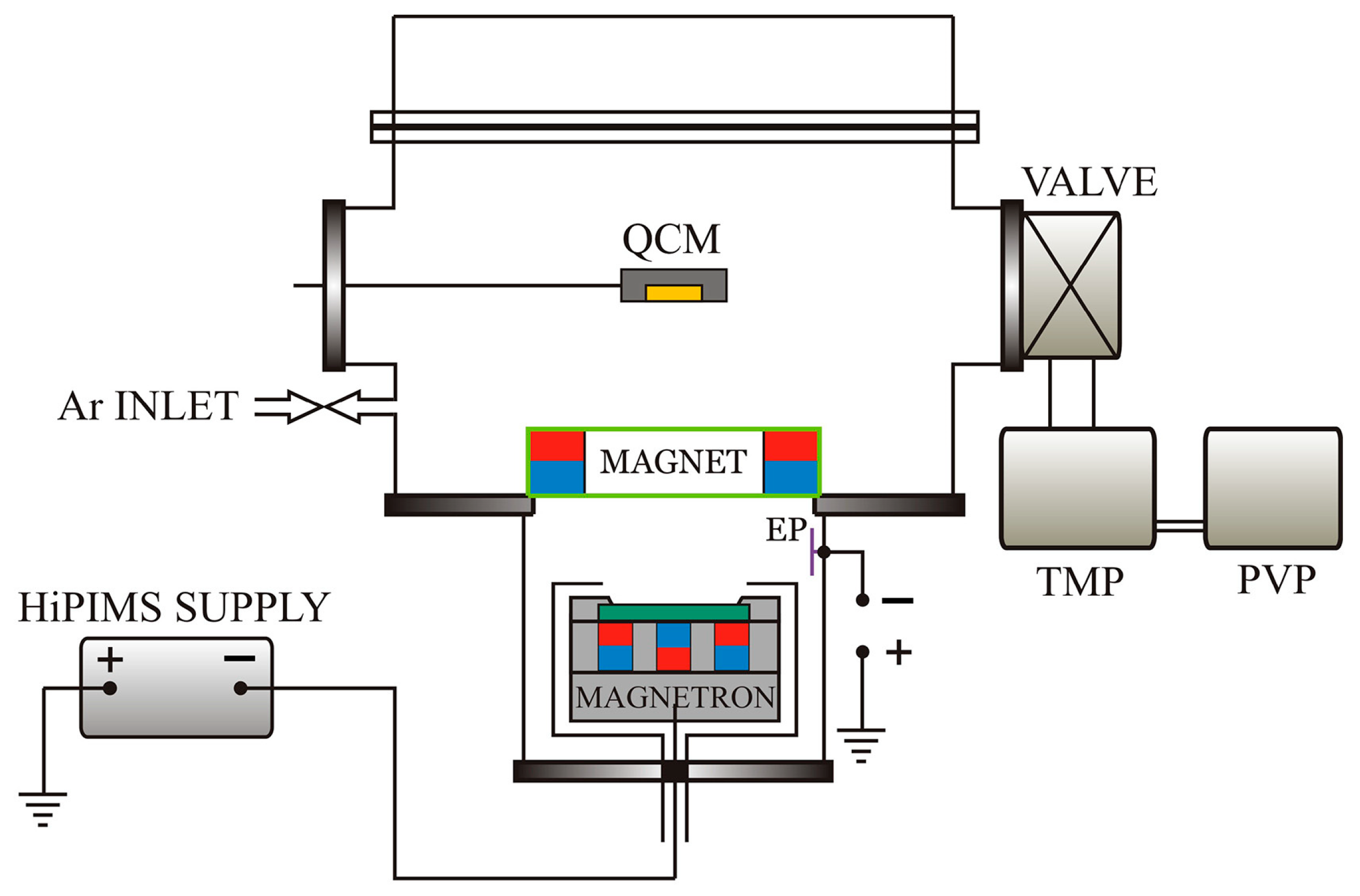
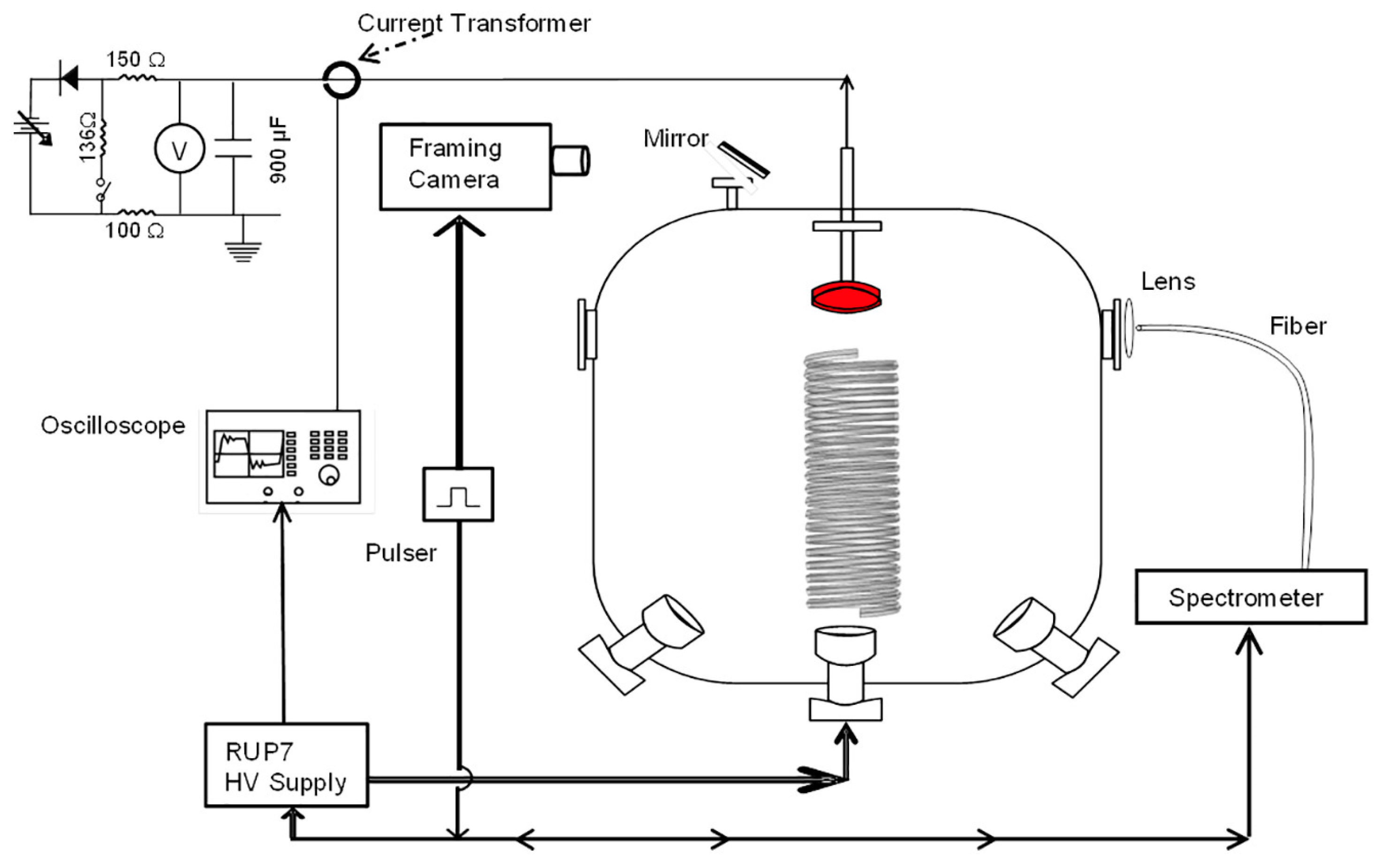
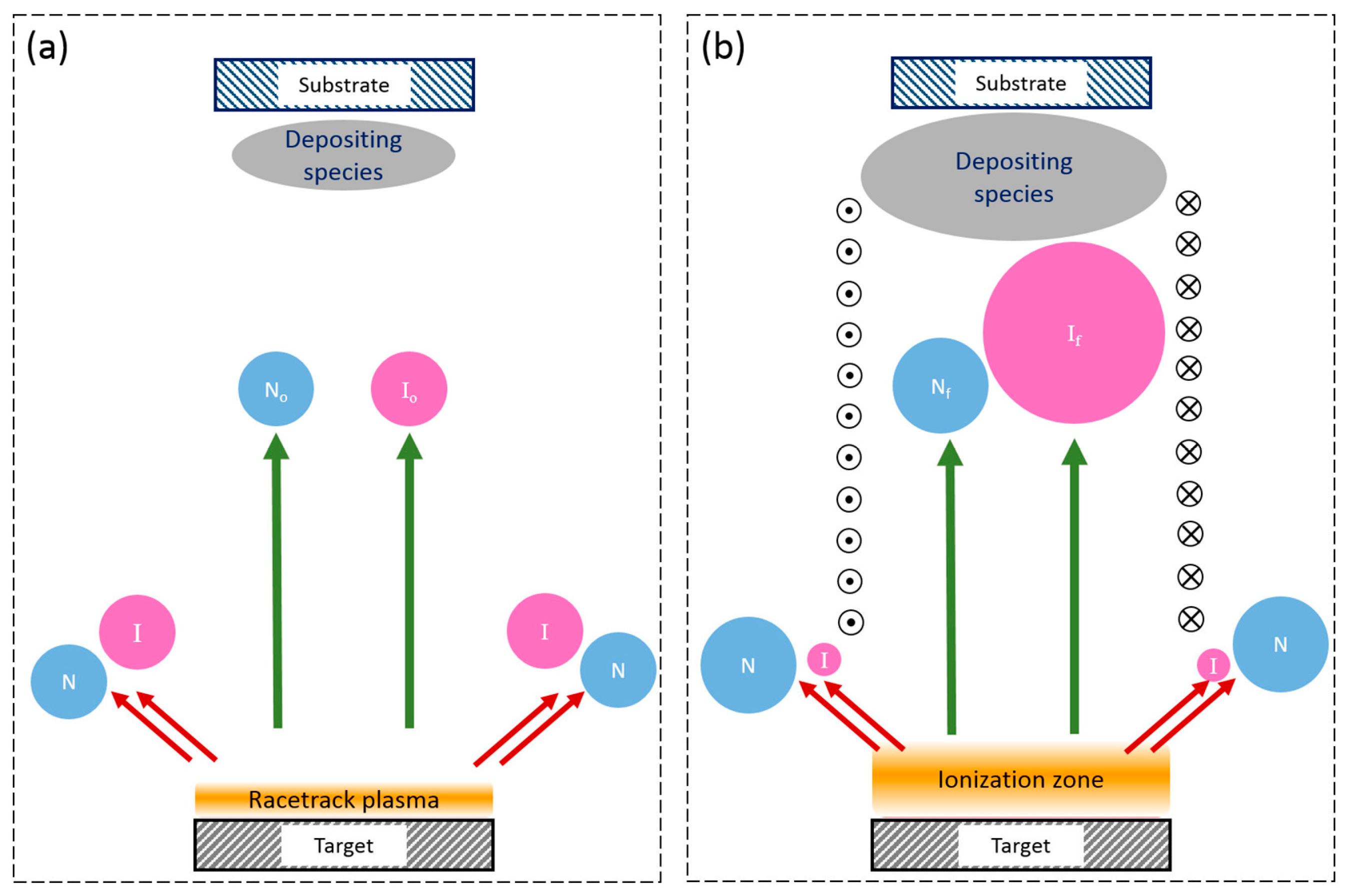
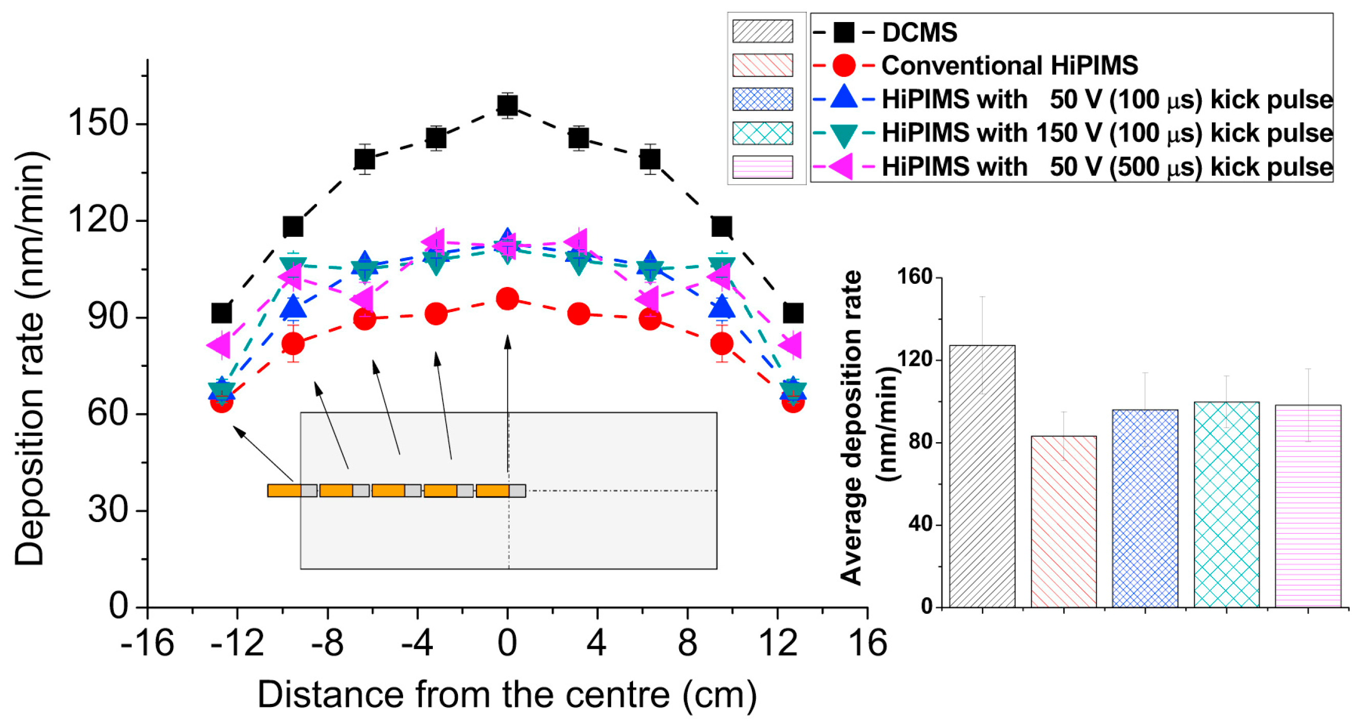
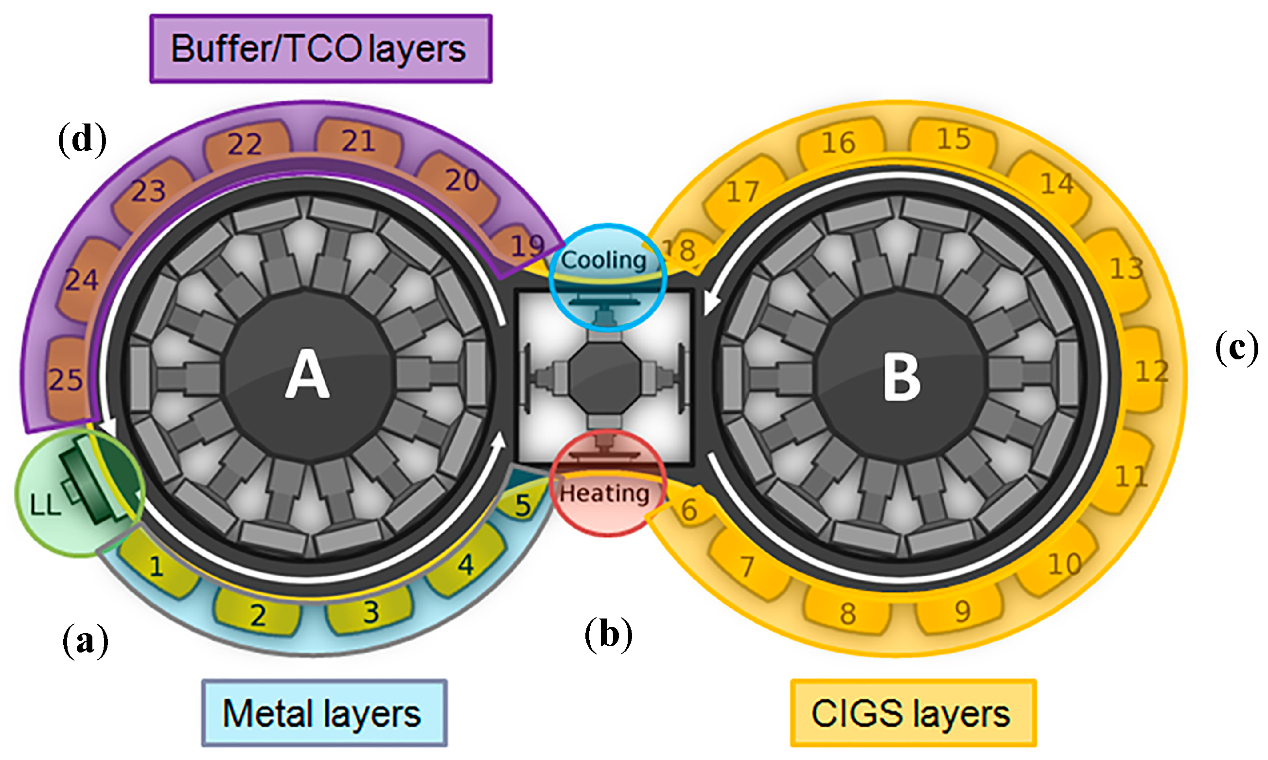
3.2. Improvements and Applications of External Devices
3.3. Considerations Using CFD Simulation
4. Concluding Remarks
Author Contributions
Funding
Acknowledgments
Conflicts of Interest
Nomenclature
| AC-MF | Alternating Current—Mid Frequency |
| BPDMS | Reactive Bipolar Pulsed Dual MS |
| CFD | Computational Fluid Dynamics |
| CIGS | Copper Indium Gallium Selenide |
| CNC | Computer numerical control |
| CVD | Chemical Vapour Deposition |
| DAS | Dual Anode Sputtering |
| DC | Direct Current |
| DCMS | Direct Current Magnetron Sputtering |
| DMS | Dual Magnetron Sputtering |
| DSMC | Direct Simulation Monte Carlo |
| E-Beam | Electron Beam Gun |
| FEM | Finite Elements Methods |
| HiPIMS | High Power Impulse Magnetron Sputtering |
| HPPMS | High-Power Pulsed Magnetron Sputtering |
| MEP | Magnetically Enhanced Plasma |
| MF | Mid Frequency |
| MPPMS | Modulated Pulsed Power MS |
| MS | Magnetron Sputtering |
| PAPVD | PVD Plasma Assisted |
| PEMS | Plasma enhanced magnetron sputtering |
| PVD | Physical Vapour Deposition |
| RF | Radio Frequency |
| TCP | Transparent Conductive Oxide |
| UBMS | Unbalanced Magnetron Sputtering |
References
- Berghaus, B. Improvements in and Related to the Coating of Articles by Means of Thermally Vapourized Material. UK Patent 510992, 1938. [Google Scholar]
- Powell, C.F.; Oxley, J.H.; Blocher, J.M. Vapour Deposition; John Wiley & Sons: New York, NY, USA, 1966. [Google Scholar]
- Holmberg, K.; Matthews, A. Coatings Tribology: Properties, Techniques and Applications in Surface Engineering; Elsevier Science: Amsterdam, The Netherlands, 1994; p. 440. [Google Scholar]
- Tracton, A.A. Coatings Technology: Fundamentals, Testing, and Processing Techniques; CRC Press: Boca Raton, FL, USA, 2007; pp. 238–284. [Google Scholar]
- Mattox, D.M. Handbook of Physical Vapor Deposition (PVD) Processing Film Formation, Adhesion, Surface Preparation and Contamination Control; Knovel: Norwich, NY, USA, 1998. [Google Scholar]
- Silva, F.J.G.; Neto, M.A.; Fernandes, A.J.S.; Costa, F.M.; Oliveira, F.J.; Silva, R.F. Adhesion and wear behaviour of NCD coatings on Si3N4 by micro-abrasion tests. J. Nanosci. Nanotechnol. 2009, 9, 3938–3943. [Google Scholar] [CrossRef] [PubMed]
- Martinho, R.P.; Silva, F.J.G.; Alexandre, R.J.D.; Baptista, A.P.M. TiB2 Nanostructured coating for GFRP injection moulds. J. Nanosci. Nanotechnol. 2011, 11, 5374–5382. [Google Scholar] [CrossRef] [PubMed]
- Musil, J. Flexible hard nanocomposite coatings. RSC Adv. 2015, 5, 60482–60495. [Google Scholar] [CrossRef]
- Veprek, S.; Veprek-Heijman, M.G.J.; Karvankova, P.; Prochazka, J. Different approaches to super hard coatings and nanocomposites. Thin Solid Films 2005, 476, 1–29. [Google Scholar] [CrossRef]
- Yang, Q.; Zhao, L.R. Microstructure, mechanical and tribological properties of novel multi-component nanolayered nitride coatings. Surf. Coat. Technol. 2005, 200, 1709–1713. [Google Scholar] [CrossRef]
- Martinho, R.P.; Andrade, M.F.C.; Silva, F.J.G.; Alexandre, R.J.D.; Baptista, A.P.M. Microabrasion wear behaviour of TiAlCrSiN nanostructured coatings. Wear 2009, 267, 1160–1165. [Google Scholar] [CrossRef]
- Silva, F.J.G.; Martinho, R.P.; Baptista, A.P.M. Characterization of laboratory and industrial CrN/CrCN/diamond-like carbon coatings. Thin Solid Films 2014, 550, 278–284. [Google Scholar] [CrossRef]
- Rubshtein, A.P.; Vladimirov, A.B.; Korkh, Y.V.; Ponosov, Y.S.; Plotnikov, S.A. The composition, structure and surface properties of the titanium-carbon coatings prepared by PVD technique. Surf. Coat. Technol. 2017, 309, 680–686. [Google Scholar] [CrossRef]
- Silva, F.J.G.; Martinho, R.P.; Alexandre, R.; Baptista, A.M. Wear resistance of TiAlSiN thin coatings. J. Nanosci. Nanotechnol. 2012, 12, 9094–9101. [Google Scholar] [CrossRef] [PubMed]
- Sam, Z. Thin Films and Coatings: Toughening and Toughness Characterization, 1st ed.; CRC Press: Boca Raton, FL, USA, 2015; pp. 377–463. [Google Scholar]
- Mubarak, A.M.A.; Hamzah, E.H.E.; Tofr, M.T.M. Review of Physical Vapour Deposition (PVD) Techniques for Hard Coating. Jurnal Mekanikal 2005, 20, 42–51. [Google Scholar]
- Mattox, D.M. Handbook of Physical Vapor Deposition (PVD) Processing; William Andrew: Amsterdam, The Netherlands, 2010; p. 792. [Google Scholar]
- Holmberg, K.; Matthews, A. Coatings Tribology: Properties, Mechanisms, Techniques and Applications in Surface Engineering, 2nd ed.; Elsevier: Amsterdam, The Netherlands, 2009; p. 576. [Google Scholar]
- Tracton, A.A. Coatings Technology Handbook, 3rd ed.; CRC Press: Boca Raton, FL, USA, 2006. [Google Scholar]
- Martin, P.M. Handbook of Deposition Technologies for Films and Coatings, 3rd ed.; Elsevier: Amsterdam, The Netherlands, 2010. [Google Scholar]
- Mattox, D.M. The Foundations of Vacuum Coating Technology; Noyes Publications: Norwich, UK, 2003. [Google Scholar]
- Silva, F.J.G.; Baptista, A.P.M.; Pereira, E.; Teixeira, V.; Fan, Q.H.; Fernandes, A.J.S.; Costa, F.M. Microwave plasma chemical vapour deposition diamond nucleation on ferrous substrates with Ti and Cr interlayers. Diam. Relat. Mater. 2002, 11, 1617–1622. [Google Scholar] [CrossRef] [Green Version]
- Silva, F.J.G. Nanoindentation on Tribological Coatings. In Applied Nanoindentation in Advanced Materials; Tiwari, A., Natarajan, S., Eds.; Wiley: New York, NY, USA, 2017; pp. 111–133. [Google Scholar]
- Silva, F.J.G.; Fernandes, A.J.S.; Costa, F.M.; Teixeira, V.; Baptista, A.P.M.; Pereira, E. Tribological behavior of CVD diamond films on steel substrates. Wear 2003, 255, 846–853. [Google Scholar] [CrossRef]
- Damm, D.D.; Contin, A.; Barbieri, F.C.; Trava-Airoldi, V.J.; Barquete, D.M.; Corat, E.J. Interlayers applied to CVD diamond deposition on steel substrate: A review. Coatings 2017, 7, 141. [Google Scholar] [CrossRef]
- Trucchi, D.M.; Bellucci, A.; Girolami, M.; Mastellone, M.; Orlando, S. Surface texturing of CVD diamond assisted by ultra short laser pulses. Coating 2017, 7, 185. [Google Scholar] [CrossRef]
- Voottipruex, P.; Bergado, D.T.; Lam, L.G.; Hino, T. Back-analyses of flow parameters of PVD improved soft Bangkok clay with and without vacuum preloading from settlement data and numerical simulations. Geotext. Geomembr. 2014, 42, 457–467. [Google Scholar] [CrossRef]
- Bobzin, K.; Brinkmann, R.; Mussenbrock, T.; Bagcivan, N.; Brugnara, R.; Schäfer, M.; Trieschmann, J. Continuum and kinetic simulations of the neutral gas flow in an industrial physical vapor deposition reactor. Surf. Coat. Technol. 2013, 237, 176–181. [Google Scholar] [CrossRef] [Green Version]
- Kapopara, J.; Mengar, A.; Chauhan, K.; Rawal, S. CFD Analysis of Sputtered TiN Coating. Mater. Today Proc. 2017, 4, 9390–9393. [Google Scholar] [CrossRef]
- Kapopara, J.M.; Mengar, A.R.; Chauhan, K.V.; Patel, N.P.; Rawal, S.K. Modelling and analysis of sputter deposited ZrN coating by CFD. In Proceedings of the IConAMMA 2016 International Conference on Advances in Materials and Manufacturing Applications, Bangalore, India, 14–16 July 2016; p. 012205. [Google Scholar]
- Skordaris, G.; Bouzakis, K.; Kotsanis, T.; Charalampous, P.; Bouzakis, E.; Breidenstein, B.; Bergmann, B.; Denkena, B. Effect of PVD film’s residual stresses on their mechanical properties, brittleness, adhesion and cutting performance of coated tools. CIRP J. Manuf. Sci. Technol. 2017, 18, 145–151. [Google Scholar] [CrossRef]
- Skordaris, G.; Bouzakis, K.; Kotsanis, T.; Charalampous, P.; Bouzakis, E.; Lemmer, O.; Bolz, S. Film thickness effect on mechanical properties and milling performance of nano-structured multilayer PVD coated tools. Surf. Coat. Technol. 2016, 307, 452–460. [Google Scholar] [CrossRef]
- Fox-Rabinovich, G.; Paiva, J.M.; Gershman, I.; Aramesh, M.; Cavelli, D.; Yamamoto, K.; Dosbaeva, G.; Veldhuis, S. Control of self-organized criticality through adaptivebehavior of nano-structured thin film coatings. Entropy 2016, 18, 290. [Google Scholar] [CrossRef]
- Hoche, H.; Groß, S.; Oechsner, M. Development of new PVD coatings for magnesium alloys with improved corrosion properties. Surf. Coat. Technol. 2014, 259, 102–108. [Google Scholar] [CrossRef]
- Korhonena, H.; Syväluoto, A.; Leskinen, J.T.T.; Lappalainen, R. Optically transparent and durable Al2O3 coatings for harsh environments by ultra short pulsed laser deposition. Opt. Laser Technol. 2018, 98, 373–384. [Google Scholar] [CrossRef]
- Inspektor, A.; Salvador, P.A. Architecture of PVD coatings for metalcutting applications: A review. Surf. Coat. Technol. 2014, 257, 138–153. [Google Scholar] [CrossRef]
- Momeni, S.; Tillmann, W. Investigation of these lf-healing sliding wear characteristics of NiTi-based PVD coatings on tool steel. Wear 2016, 368, 53–59. [Google Scholar] [CrossRef]
- Michailidis, N. Variations in the cutting performance of PVD-coated tools in milling Ti6Al4V, explained through temperature-dependent coating properties. Surf. Coat. Technol. 2016, 304, 325–329. [Google Scholar] [CrossRef]
- Gouveia, R.M.; Silva, F.J.G.; Reis, P.; Baptista, A.P.M. Machining duplex stainless steel: Comparative study regarding end mill coated tools. Coatings 2016, 6, 51. [Google Scholar] [CrossRef]
- Martinho, R.P.; Silva, F.J.G.; Baptista, A.P.M. Cutting forces and wear analysis of Si3N4 diamond coated tools in high speed machining. Vacuum 2008, 82, 1415–1420. [Google Scholar] [CrossRef] [Green Version]
- Nunes, V.; Silva, F.J.G.; Andrade, M.F.; Alexandre, R.; Baptista, A.P.M. Increasing the lifespan of high-pressure die cast molds subjected to severe wear. Surf. Coat. Technol. 2017, 332, 319–331. [Google Scholar] [CrossRef]
- Fernandes, L.; Silva, F.J.G.; Andrade, M.F.; Alexandre, R.; Baptista, A.P.M.; Rodrigues, C. Increasing the stamping tools lifespan by using Mo and B4C PVD coatings. Surf. Coat. Technol. 2017, 325, 107–119. [Google Scholar] [CrossRef]
- Vereschaka, A.; Kataeva, E.; Sitnikov, N.; Aksenenko, A.; Oganyan, G.; Sotova, C. Influence of Thickness of Multilayered Nano-Structured Coatings Ti-TiN-(TiCrAl)N and Zr-ZrN-(ZrCrNbAl)N on Tool Life of Metal Cutting Tools at Various Cutting Speeds. Coatings 2018, 8, 44. [Google Scholar] [CrossRef]
- Baptista, A.; Silva, F.J.G.; Pinto, G.; Porteiro, J.; Míguez, J.; Fernandes, L. On the physical vapour deposition (PVD) process evolution. Procedia Manuf. 2018, in press. [Google Scholar]
- Pinto, G.; Silva, F.J.G.; Baptista, A.; Porteiro, J.; Míguez, J.; Fernandes, L. A critical review on the numerical simulation related to physical vapour deposition. Procedia Manuf. 2018, in press. [Google Scholar]
- Maity, S. Optimization of processing parameters of in-situ polymerization of pyrrole on woollen textile to improve its thermal conductivity. Prog. Org. Coat. 2017, 107, 48–53. [Google Scholar] [CrossRef]
- Kim, M.; Kim, S.; Kim, T.; Lee, D.K.; Seo, B.K.; Lim, C.S. Mechanical and thermal properties of epoxy composites containing zirconium oxide impregnated halloysite nanotubes. Coatings 2017, 7, 231. [Google Scholar] [CrossRef]
- Hu, N.; Khan, M.; Wang, Y.; Song, X.; Lin, C.; Chang, C.; Zeng, Y. Effect of Microstructure on the Thermal Conductivity of Plasma Sprayed Y2O3 Stabilized Zirconia (8% YSZ). Coatings 2017, 7, 198. [Google Scholar] [CrossRef]
- Silva, F.J.G.; Casais, R.C.B.; Martinho, R.P.A.; Baptista, P.M. Mechanical and tribological characterization of TiB2 thin films. J. Nanosci. Nanotechnol. 2012, 12, 9187–9194. [Google Scholar] [CrossRef] [PubMed]
- Silva, F.J.G.; Martinho, R.P.; Andrade, M.; Baptista, A.P.M.; Alexandre, R. Improving the wear resistance of moulds for the injection of glass fibre–reinforced plastics using PVD coatings: A comparative study. Coatings 2017, 7, 28. [Google Scholar] [CrossRef]
- Abdullah, M.Z.B.; Ahmad, M.A.; Abdullah, A.N.; Othman, M.H.; Hussain, P.; Zainuddin, A. Metal release of multilayer coatings by physical vapour deposition (PVD). Procedia Eng. 2016, 148, 254–260. [Google Scholar] [CrossRef]
- Imbeni, V.; Martini, C.; Lanzoni, E.; Poli, G.; Hutchings, I.M. Tribological behaviour of multi-layered PVD nitride coatings. Wear 2001, 251, 997–1002. [Google Scholar] [CrossRef]
- Wasa, K.; Kitabatake, M.; Adachi, H. Thin Film Materials Technology: Sputtering of Compound Materials; William Andrew: Amsterdam, The Netherlands, 2004. [Google Scholar]
- Decher, G.; Schlenoff, J.B. Multilayer Thin Films: Sequential Assembly of Nanocomposite Materials; Wiley: Weinheim, Germany, 2003. [Google Scholar]
- Silva, F.J.G. Estudo da Estrutura e Comportamento Tribológico de Revestimentos Duros e Ultra-Duros Executados no Vácuo. Master’s Thesis, FEUP, Porto, Portugal, 2001. (In Portuguese). [Google Scholar]
- Bass, R.B.; Lichtenberger, L.T.; Lichtenberger, A.W. Effects of Substrate Preparation on the Stress of Nb Thin Films. IEEE Trans. Appl. Supercond. 2003, 13, 3298–3300. [Google Scholar] [CrossRef]
- Karabacak, T.; Senkevich, J.J.; Wang, G.C.; Lu, T.M. Stress reduction in sputter deposited films using nanostructured compliant layers by high working-gas pressures. J. Vac. Sci. Technol. A 2005, 23, 986–990. [Google Scholar] [CrossRef]
- Estrada-Martínez, J.L.; Banda, J.A.M.; García, U.P.; Muñoz, J.R.; Muñoz, J.L.F.; Lira, M.M.; Ángel, O.Z. Set-up method on properties of BaxSr1−xTiO3 thin films deposited by RF-magnetron co-sputtering by projecting temperature and stoichiometric effect. Preprints 2017, 2017100043. [Google Scholar] [CrossRef]
- Plummer, J.D.; Deal, M.; Griffin, P.B. Silicon VLSI Technology: Fundamentals, Practice, and Modeling; Prentice Hall: Upper Saddle River, NJ, USA, 2000; p. 817. [Google Scholar]
- Rother, B.; Ebersbach, G.; Gabriel, H.M. Substrate-rotation systems and productivity of industrial PVD processes. Surf. Coat. Technol. 1999, 116–119, 694–698. [Google Scholar] [CrossRef]
- Martinho, R.P. Revestimentos PVD Mono e Multicamada Para Moldes Utilizados na Injecção de Plásticos Reforçados. Master’s Thesis, FEUP, Porto, Portugal, 2009. (In Portuguese). [Google Scholar]
- Steimann, P.A.; Hintermann, H.E. Adhesion of TiC and Ti(C, N) coatings on steel. J. Vac. Sci. Technol. A 1985, 3, 2394–2400. [Google Scholar] [CrossRef]
- Barshilia, H.C.; Ananth, A.; Khan, J.; Srinivas, G. Ar + H2 plasma etching for improved adhesion of PVD coatings on steel substrates. Vacuum 2012, 86, 1165–1173. [Google Scholar] [CrossRef]
- Lente, H.V.; Til, J.I.V. Articulation of sustainability in the emerging field of nanocoatings. J. Clean. Prod. 2008, 16, 967–976. [Google Scholar] [CrossRef]
- Gassner, M.; Figueiredo, M.R.; Schalk, N.; Franz, R.; Weiß, C.; Rudigier, H.; Holzschuh, H.; Bürgind, W.; Pohler, M.; Czettl, C.; Mitterer, C. Energy consumption and material fluxes in hard coating deposition processes. Surf. Coat. Technol. 2016, 299, 49–55. [Google Scholar] [CrossRef]
- Klocke, F.; Döbbeler, B.; Binder, M.; Kramer, N.; Grüter, R.; Lung, D. Ecological evaluation of PVD and CVD coating systems in metal cutting processes. In Proceedings of the 11th Global Conference on Sustainable Manufacturing, Berlin, Germany, 23–25 September 2013. [Google Scholar]
- Hogmark, S.; Jacobson, S.; Larsson, M. Design and evaluation of tribological coatings. Wear 2000, 246, 20–33. [Google Scholar] [CrossRef]
- Jiang, X.; Yang, F.C.; Chenc, W.C.; Lee, J.W.; Chang, C.L. Effect of nitrogen-argon flow ratio on the microstructural and mechanical properties of AlSiN thin films prepared by high power impulse magnetron sputtering. Surf. Coat. Technol. 2017, 320, 138–145. [Google Scholar] [CrossRef]
- Li, B.S.; Wang, T.G.; Ding, J.; Cai, Y.; Shi, J.; Zhang, X. Influence of N2/Ar Flow Ratio on Microstructure and Properties of the AlCrSiN Coatings Deposited by High-Power Impulse Magnetron Sputtering. Coatings 2018, 8, 3. [Google Scholar] [CrossRef]
- Alamia, J.; Bolz, S.; Sarakinos, K. High power pulsed magnetron sputtering: Fundamentals and applications. J. Alloys Compd. 2009, 483, 530–534. [Google Scholar] [CrossRef]
- Rother, B.; Jehn, H.A.; Gabriel, H.M. Multilayer hard coatings by coordinated substrate rotation modes in industrial PVD deposition systems. Surf. Coat. Technol. 1996, 86–87, 207–211. [Google Scholar] [CrossRef]
- Bobzin, K.; Brögelmann, T.; Kalscheuer, C.; Liang, T. High-rate deposition of thick (Cr,Al) ON coatings by high speed physical vapor deposition. Surf. Coat. Technol. 2017, 322, 152–162. [Google Scholar] [CrossRef]
- Liu, M.J.; Zhang, M.; Zhang, Q.; Yang, G.J.; Li, C.X.; Li, C.J. Gaseous material capacity of open plasma jet in plasma spray-physical vapor deposition process. Appl. Surf. Sci. 2018, 428, 877–884. [Google Scholar] [CrossRef]
- Kolzer Vacuum Coating Equipment. Available online: http://www.kolzer.com (accessed on 15 July 2018).
- CemeCon—The Tool Coating. Available online: http://www.cemecon.de/en (accessed on 15 July 2018).
- High Performance Coatings for Tools and Components Oerlikon Balzers. Available online: https://www.oerlikon.com (accessed on 15 July 2018).
- Teer Coatings. Available online: http://www.teercoatings.co.uk/index.php?page=13 (accessed on 4 October 2018).
- Panjana, M.; Cekada, M.; Panjan, P.; Zalar, A.; Peterman, T. Sputtering simulation of multilayer coatings in industrial PVD system with three-fold rotation. Vacuum 2008, 82, 158–161. [Google Scholar] [CrossRef]
- Mitterer, C. PVD and CVD hard coatings. In Comprehensive Hard Materials; Sarin, V.K., Ed.; Elsevier: Amsterdam, The Netherlands, 2014; Volume 2, pp. 449–467. [Google Scholar] [CrossRef]
- Linss, V. Comparison of the large-area reactive sputter processes of ZnO: Al and ITO using industrial size rotatable targets. Surf. Coat. Technol. 2016, 290, 43–57. [Google Scholar] [CrossRef]
- Linss, V. Challenges in the industrial deposition of transparent conductive oxide materials by reactive magnetron sputtering from rotatable targets. Thin Solid Films 2017, 634, 149–154. [Google Scholar] [CrossRef]
- Rizzo, A.; Valerini, D.; Capodieci, L.; Mirenghi, L.; Benedetto, F.D.; Protopapa, M.L. Reactive bipolar pulsed dual magnetron sputtering of ZrN films: The effect of duty cycle. Appl. Surf. Sci. 2018, 427, 994–1002. [Google Scholar] [CrossRef]
- Wackelgard, E.; Hultmark, G. Industrially sputtered solar absorber surface. Sol. Energy Mater. Sol. Cells 1998, 54, 165–170. [Google Scholar] [CrossRef]
- Rösemann, N.; Ortner, K.; Petersen, J.; Bäke, M.; Bräuer, G.; Rösler, J. Microstructure of gas flow sputtered thermal barrier coatings: Influence of bias voltage. Surf. Coat. Technol. 2017, 332, 22–29. [Google Scholar] [CrossRef]
- Rösemann, N.; Ortner, K.; Petersen, J.; Schadow, T.; Bäker, M.; Bräuer, G.; Rösler, J. Influence of bias voltage and oxygen flow rate on morphology and crystallographic properties of gas flow sputtered zirconia coatings. Surf. Coat. Technol. 2015, 276, 668–676. [Google Scholar] [CrossRef]
- Weirather, T.; Czettl, C.; Polcik, P.; Kathrein, M.; Mitterer, C. Industrial-scale sputter deposition of Cr1−xAlxN coatings with 0.21 ≤ x ≤ 0.74 from segmented targets. Surf. Coat. Technol. 2013, 232, 303–310. [Google Scholar] [CrossRef]
- Bagcivan, N.; Bobzin, K.; Theiß, S. (Cr1−xAlx)N: A comparison of direct current, middle frequency pulsed and high power pulsed magnetron sputtering for injection molding components. Thin Solid Films 2013, 528, 180–186. [Google Scholar] [CrossRef]
- Anders, A. A review comparing cathodic arcs and high power impulse magnetron sputtering (HiPIMS). Surf. Coat. Technol. 2014, 257, 308–325. [Google Scholar] [CrossRef] [Green Version]
- Gudmundsson, J.T.; Brenning, N.; Lundin, D.; Helmersson, U. High power impulse magnetron sputtering discharge. J. Vac. Sci. Technol. A 2012, 30, 030801. [Google Scholar] [CrossRef] [Green Version]
- Lin, J.L.; Sproul, W.D.; Moore, J.J.; Wu, Z.L.; Lee, S.; Chistyakov, R.; Abraham, B. Recent advances in modulated pulsed power magnetron sputtering for surface engineering. JOM 2011, 63, 48–58. [Google Scholar] [CrossRef]
- Yazdi, M.; Lomello, F.; Wang, J.; Sanchette, F.; Dong, Z.; White, T.; Wouters, Y.; Schuster, F.; Billard, A. Properties of TiSiN coatings deposited by hybrid HiPIMS and pulsed-DC magnetron co-sputtering. Vacuum 2014, 109, 43–51. [Google Scholar] [CrossRef]
- Alami, J.; Maric, Z.; Busch, H.; Klein, F.; Grabowy, U.; Kopnarski, M. Enhanced ionization sputtering: A concept for superior industrial coatings. Surf. Coat. Technol. 2014, 255, 43–51. [Google Scholar] [CrossRef]
- Wu, Z.L.; Li, Y.G.; Wu, B.; Lei, M.K. Effect of microstructure on mechanical and tribological properties of TiAlSiN nanocomposite coatings deposited by modulated pulsed power magnetron sputtering. Thin Solid Films 2015, 597, 197–205. [Google Scholar] [CrossRef]
- Oliveira, J.C.; Ferreira, F.; Anders, A.; Cavaleiro, A. Reduced atomic shadowing in HiPIMS: Role of the thermalized metal ions. Appl. Surf. Sci. 2018, 433, 934–944. [Google Scholar] [CrossRef]
- Lin, J.; Wei, R. A comparative study of thick TiSiCN nanocomposite coatings deposited by dcMS and HiPIMS with and without PEMS assistance. Surf. Coat. Technol. 2018, 338, 84–95. [Google Scholar] [CrossRef]
- Bandorf, R.; Sittinger, V.; Bräuer, G. High Power Impulse Magnetron Sputtering–HIPIMS. In Comprehensive Materials Processing, 1st ed.; Hashmi, S., Ed.; Elsevier: Amsterdam, The Netherlands, 2014; pp. 75–99. [Google Scholar] [CrossRef]
- Li, C.; Tian, X.; Gong, C.; Xu, J. The improvement of high power impulse magnetron sputtering performance by an external unbalanced magnetic field. Vacuum 2016, 133, 98–104. [Google Scholar] [CrossRef]
- Li, C.; Tian, X.; Gong, C.; Xu, J.; Liu, S. Synergistic enhancement effect between external electric and magnetic fields during high power impulse magnetron sputtering discharge. Vacuum 2017, 143, 119–128. [Google Scholar] [CrossRef]
- Tiron, V.; Velicu, I.L.; Mihăilă, I.; Popa, G. Deposition rate enhancement in HiPIMS through the control of magnetic field and pulse configuration. Surf. Coat. Technol. 2018, 337, 484–491. [Google Scholar] [CrossRef]
- Ganesan, R.; Akhavan, B.; Dong, X.; McKenzie, D.R.; Bilek, M.M.M. External magnetic field increases both plasma generation and deposition rate in HiPIMS. Surf. Coat. Technol. 2019, 352, 671–679. [Google Scholar] [CrossRef]
- Wu, B.; Haehnlein, I.; Shchelkanov, I.; Lain, J.M.; Patel, D.; Uhlig, J.; Jurczyk, B.; Leng, Y.; Ruzic, D.N. Cu films prepared by bipolar pulsed high power impulse magnetron sputtering. Vacuum 2018, 150, 216–221. [Google Scholar] [CrossRef]
- Bras, P.; Frisk, C.; Tempez, A.; Niemi, E.; Björkman, C.P.; Brasa, P.; Frisk, C.; Tempez, A.; Niemi, E.; Platzer-Björkman, C. Ga-grading and Solar Cell Capacitance Simulation of an industrial Cu(In,Ga)Se2 solar cell produced by an in-line. Vacuum 2017, 636, 367–374. [Google Scholar] [CrossRef]
- Tapia, E.; Iranzo, A.; Pino, F.; Rosa, F.; Salva, J. Methodology for thermal design of solar tubular reactors using CFD techniques. Int. J. Hydrog. Energy 2016, 41, 19525–19538. [Google Scholar] [CrossRef]
- Abdel-Fattah, A.; Fateen, S.; Moustafa, T.; Fouad, M. Three-dimensional CFD simulation of industrial Claus reactors. Chem. Eng. Res. Des. 2016, 112, 78–87. [Google Scholar] [CrossRef]
- Bouaouina, B.; Mastail, C.; Besnard, A.; Mareus, R.; Nita, F.; Michel, A.; Abadias, G. Nanocolumnar TiN thin film growth by oblique angle sputter-deposition: Experiments vs. simulations. Mater. Des. 2018, 160, 338–349. [Google Scholar] [CrossRef]
- Sliwa, A.; Mikuła, J.; Gołombek, K.; Tanski, T.; Kwasny, W.; Bonek, M.; Brytan, Z. Prediction of the properties of PVD/CVD coatings with the use of FEM analysis. Appl. Surf. Sci. 2016, 388, 281–287. [Google Scholar] [CrossRef]
- Venkateswara Raoa, R. The Significant Application of FEM to Evaluate the Mechanical Properties of Thin Films. Procedia Mater. Sci. 2014, 6, 1260–1265. [Google Scholar] [CrossRef]
- Bouzakis, K.; Skordaris, G.; Klocke, F.; Bouzakis, E. A FEM-based analytical–experimental method for determining strength properties gradation in coatings after micro-blasting. Surf. Coat. Technol. 2009, 203, 2946–2953. [Google Scholar] [CrossRef]
- Prades, L.; Dorado, A.; Climent, J.; Guimerà, X.; Chiva, S.; Gamisans, X. CFD modeling of a fixed-bed biofilm reactor coupling hydrodynamics and biokinetics. Chem. Eng. J. 2017, 313, 680–692. [Google Scholar] [CrossRef] [Green Version]
- Phuan, Y.; Ismail, H.; Garcia-Segura, S.; Chong, M. Design and CFD modelling of the anodic chamber of a continuous PhotoFuelCell reactor for water treatment. Process Saf. Environ. Prot. 2017, 111, 449–461. [Google Scholar] [CrossRef]
- Adebiyi, D.; Popoola, A.; Botef, I. Experimental Verification of Statistically Optimized Parameters for Low-Pressure Cold Spray Coating of Titanium. Metals 2016, 6, 135. [Google Scholar] [CrossRef]
- Silva, A.; Monteiro, C.; Souza, V.; Ferreira, A.; Jaimes, R.; Fontoura, D.; Nunhez, J. Fluid dynamics and reaction assessment of diesel oil hydrotreating reactors via CFD. Fuel Process. Technol. 2017, 166, 17–29. [Google Scholar] [CrossRef]
- Sen, S.; Lake, M.; Kroppen, N.; Farber, P.; Wilden, J.; Schaaf, Ç. Self-propagating exothermic reaction analysis in Ti/Al reactive films using experiments and computational fluid dynamics simulation. Appl. Surf. Sci. 2017, 396, 1490–1498. [Google Scholar] [CrossRef]
- Depla, D.; Leroy, W.P. Magnetron sputter deposition as visualized by Monte Carlo modeling. Thin Solid Films 2012, 520, 6337–6354. [Google Scholar] [CrossRef]
- Trieschmann, J. Neutral gas simulation on the influence of rotating spokes on gas rare faction in high-power impulse magnetron sputtering. Contrib. Plasma Phys. 2017, 58, 394–403. [Google Scholar] [CrossRef]


| Parameters | Sputtering | Evaporation |
|---|---|---|
| Vacuum | Low | High |
| Deposition rate | Low (except for pure metals and dual magnetron) | High (up to 750,000 A min−1) |
| Adhesion | High | Low |
| Absorption | High | Less absorbed gas into the film |
| Deposited species energy | High (1–100 eV) | Low (∼0.1–0.5 eV) |
| Homogeneous film | More | Less |
| Grain size | Smaller | Bigger |
| Atomized particles | More Dispersed | Highly directional |
© 2018 by the authors. Licensee MDPI, Basel, Switzerland. This article is an open access article distributed under the terms and conditions of the Creative Commons Attribution (CC BY) license (http://creativecommons.org/licenses/by/4.0/).
Share and Cite
Baptista, A.; Silva, F.; Porteiro, J.; Míguez, J.; Pinto, G. Sputtering Physical Vapour Deposition (PVD) Coatings: A Critical Review on Process Improvement and Market Trend Demands. Coatings 2018, 8, 402. https://0-doi-org.brum.beds.ac.uk/10.3390/coatings8110402
Baptista A, Silva F, Porteiro J, Míguez J, Pinto G. Sputtering Physical Vapour Deposition (PVD) Coatings: A Critical Review on Process Improvement and Market Trend Demands. Coatings. 2018; 8(11):402. https://0-doi-org.brum.beds.ac.uk/10.3390/coatings8110402
Chicago/Turabian StyleBaptista, Andresa, Francisco Silva, Jacobo Porteiro, José Míguez, and Gustavo Pinto. 2018. "Sputtering Physical Vapour Deposition (PVD) Coatings: A Critical Review on Process Improvement and Market Trend Demands" Coatings 8, no. 11: 402. https://0-doi-org.brum.beds.ac.uk/10.3390/coatings8110402